Report an Error


ZOTAC P102-100
- ZT-M10200A-10B
- Graphics Processor
- GP102
- Cores
- 3200
- TMUs
- 200
- ROPs
- 80
- Memory Size
- 5 GB
- Memory Type
- GDDR5X
- Bus Width
- 320 bit

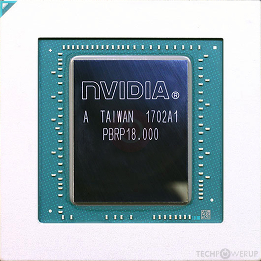
GPU
Graphics Processor
Graphics Card
Clock Speeds
- Base Clock
- 1582 MHz
- Boost Clock
- 1683 MHz
- Memory Clock
-
1376 MHz
11 Gbps effective
Memory
- Memory Size
- 5 GB
- Memory Type
- GDDR5X
- Memory Bus
- 320 bit
- Bandwidth
- 440.3 GB/s
Render Config
- Shading Units
- 3200
- TMUs
- 200
- ROPs
- 80
- SM Count
- 25
- L1 Cache
- 48 KB (per SM)
- L2 Cache
- 2.5 MB
Theoretical Performance
- Pixel Rate
- 134.6 GPixel/s
- Texture Rate
- 336.6 GTexel/s
- FP16 (half)
- 168.3 GFLOPS (1:64)
- FP32 (float)
- 10.77 TFLOPS
- FP64 (double)
- 336.6 GFLOPS (1:32)
Board Design
- Slot Width
- Dual-slot
- Length
267 mm
215 mm
10.5 inches
8.5 inches
- TDP
- 250 W
- Suggested PSU
- 600 W
- Outputs
- No outputs
- Power Connectors
- 2x 8-pin
- Board Number
- PG611 SKU 100
Graphics Features
- DirectX
- 12 (12_1)
- OpenGL
- 4.6
- OpenCL
- 3.0
- Vulkan
- 1.3
- CUDA
- 6.1
- Shader Model
- 6.8
GP102 GPU Notes
| NVENC: 6th Gen NVDEC: 3rd Gen PureVideo HD: VP8 VDPAU: Feature Set H Latest Drivers: Windows 7 / 8 / 8.1 (x32 / x64): GeForce Release 391.35 / 474.89 Quadro Release R390 U9 (392.37) / R440 U4 (441.66) Data Center Release 427.11 Windows 10 / 11 (x32 / x64): GeForce Release 391.35 / Latest Quadro Release R390 U9 (392.37) / Latest Data Center Release: Latest |
Other retail boards based on this design (2)
| Name | GPU Clock | Boost Clock | Memory Clock | Other Changes |
|---|---|---|---|---|
| 1582 MHz | 1683 MHz | 1376 MHz | 215 mm/8.5 inches | |
|
ZOTAC P102-100

|
1582 MHz | 1683 MHz | 1376 MHz | 215 mm/8.5 inches |

Nov 13th, 2024 02:12 EST
change timezone
Latest GPU Drivers
New Forum Posts
- 9800x 3d vs 12900k - Battle of the Century (47)
- Playing with a shiny new msi laptop tonight. Summit 13 AI+ Evo (0)
- Post your Speedometer 3.0 Score (83)
- It's nearly 2025 and the selection of 4K monitors remains abysmal. Let's discuss this sad state of affairs. (131)
- Ghetto Mods (4476)
- Shadow Of The Tomb Raider - CPU Performance and general game benchmark discussions (535)
- Inconsistent POSTing on PC ( already replaced multiple parts) (54)
- Your PC ATM (35012)
- Crossfire R9 Fury not available (22)
- The Official Linux/Unix Desktop Screenshots Megathread (748)
Popular Reviews
- AMD Ryzen 7 9800X3D Review - The Best Gaming Processor
- NVIDIA App v1.0 Review
- Team Group A440 Lite 2 TB Review
- FiiO Industrial Park/Factory Tour + Interview with Founder
- Upcoming Hardware Launches 2024 (Updated Nov 2024)
- MIRPH-1 Open-Back Dynamic Driver Headphones Review
- XPG Invader X Mini Review
- ID-Cooling FX360 INF AIO Review
- DDR5 Memory Performance Scaling with AMD Zen 5
- Intel Core Ultra 9 285K Review
Controversial News Posts
- AMD Falling Behind: Radeon dGPUs Absent from Steam's Top 20 (222)
- AMD Ryzen 7 9800X3D Stocks Vaporized in Retail, Being Scalped (141)
- Quick Denuvo DRM Cracks Cost Game Publishers 20% in Revenue, According to Study (136)
- AMD Introduces Next-Generation AMD Ryzen 7 9800X3D Processor, $479, Nov 7 (124)
- Apple and Samsung in the Fray to Acquire Intel: Rumor (123)
- AMD Ryzen 7 9800X3D Comes with 120W TDP, 5.20 GHz Boost, All Specs Leaked (120)
- Microsoft Offers $30 Windows 10 Security Extension for Home Users (118)
- AMD Ryzen 7 9800X3D Has the CCD on Top of the 3D V-cache Die, Not Under it (110)