Report an Error


NVIDIA Quadro FX 1700
- Graphics Processor
- G84
- Cores
- 32
- TMUs
- 16
- ROPs
- 8
- Memory Size
- 512 MB
- Memory Type
- DDR2
- Bus Width
- 256 bit

GPU

Bottom
Recommended Gaming Resolutions:
- 640x480
- 1280x720
- 1366x768
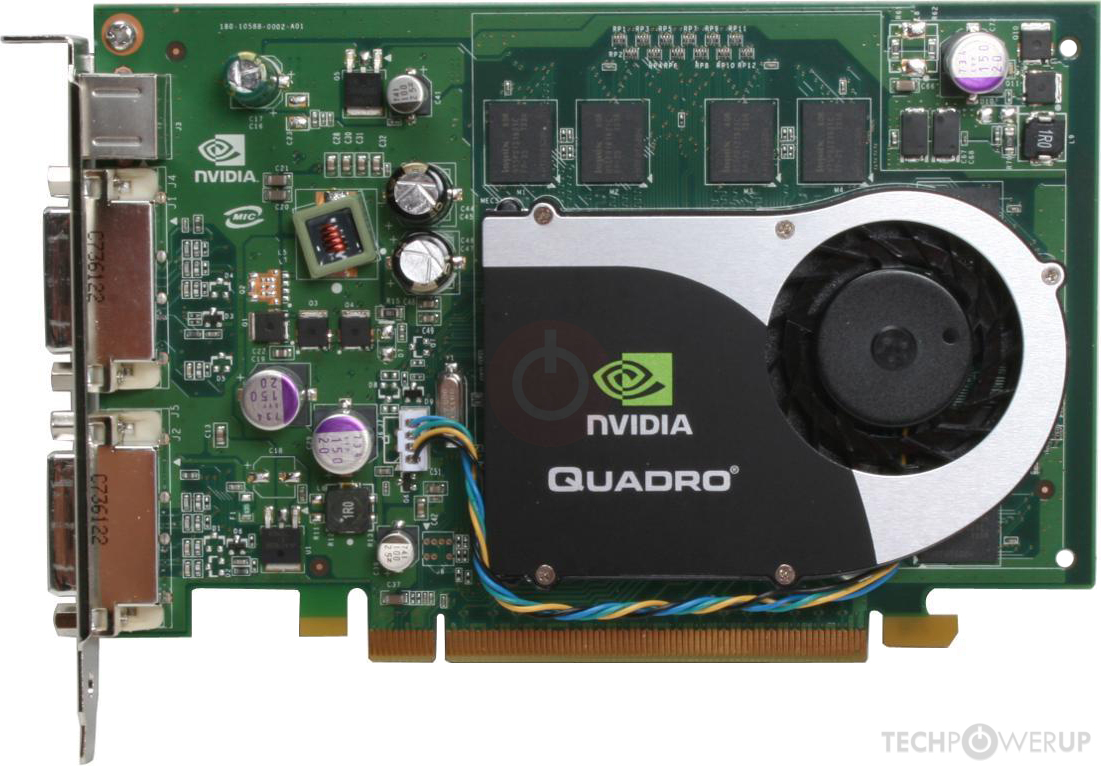
The Quadro FX 1700 was an enthusiast-class professional graphics card by NVIDIA, launched on September 12th, 2007. Built on the 80 nm process, and based on the G84 graphics processor, in its G84-875-A2 variant, the card supports DirectX 11.1. Even though it supports DirectX 11, the feature level is only 10_0, which can be problematic with many DirectX 11 & DirectX 12 titles. The G84 graphics processor is an average sized chip with a die area of 169 mm² and 289 million transistors. It features 32 shading units, 16 texture mapping units, and 8 ROPs. NVIDIA has paired 512 MB DDR2 memory with the Quadro FX 1700, which are connected using a 256-bit memory interface. The GPU is operating at a frequency of 460 MHz, memory is running at 400 MHz.
Being a single-slot card, the NVIDIA Quadro FX 1700 does not require any additional power connector, its power draw is rated at 42 W maximum. Display outputs include: 2x DVI, 1x S-Video. Quadro FX 1700 is connected to the rest of the system using a PCI-Express 1.0 x16 interface. The card measures 168 mm in length, 111 mm in width, and features a single-slot cooling solution. Its price at launch was 699 US Dollars.
Being a single-slot card, the NVIDIA Quadro FX 1700 does not require any additional power connector, its power draw is rated at 42 W maximum. Display outputs include: 2x DVI, 1x S-Video. Quadro FX 1700 is connected to the rest of the system using a PCI-Express 1.0 x16 interface. The card measures 168 mm in length, 111 mm in width, and features a single-slot cooling solution. Its price at launch was 699 US Dollars.
Graphics Processor
Graphics Card
- Release Date
- Sep 12th, 2007
- Generation
-
Quadro FX Tesla
(x700)
- Predecessor
- Quadro FX Curie
- Successor
- Quadro Fermi
- Production
- End-of-life
- Launch Price
- 699 USD
- Bus Interface
- PCIe 1.0 x16
- Reviews
- 26 in our database
Relative Performance
Based on TPU review data: "Performance Summary" at 1920x1080, 4K for 2080 Ti and faster.
Performance estimated based on architecture, shader count and clocks.
Clock Speeds
- GPU Clock
- 460 MHz
- Shader Clock
- 920 MHz
- Memory Clock
-
400 MHz
800 Mbps effective
Memory
- Memory Size
- 512 MB
- Memory Type
- DDR2
- Memory Bus
- 256 bit
- Bandwidth
- 25.60 GB/s
Render Config
- Shading Units
- 32
- TMUs
- 16
- ROPs
- 8
- SM Count
- 4
- L2 Cache
- 64 KB
Theoretical Performance
- Pixel Rate
- 3.680 GPixel/s
- Texture Rate
- 7.360 GTexel/s
- FP32 (float)
- 58.88 GFLOPS
Board Design
- Slot Width
- Single-slot
- Length
- 168 mm
6.6 inches
- Width
- 111 mm
4.4 inches
- TDP
- 42 W
- Suggested PSU
- 200 W
- Outputs
- 2x DVI
1x S-Video
- Power Connectors
- None
- Board Number
- P588 SKU 505
Graphics Features
- DirectX
- 11.1 (10_0)
- OpenGL
- 3.3
- OpenCL
- 1.1
- Vulkan
- N/A
- CUDA
- 1.1
- Shader Model
- 4.0
G84 GPU Notes
| PureVideo HD: VP2 VDPAU: Feature Set A Latest Drivers: Windows 2000: Quadro Release 261.19 Windows XP / Server 2003 x64: GeForce Release 185.81 (Notebooks) GeForce Release 340.52 Quadro Release R319 U2 (321.01) Tesla Release 258.96 Windows Vista: GeForce Release 307.83 (Notebooks) GeForce Release 342.01 Quadro Release R340 U15 (342.01) Tesla Release 258.96 Windows 7 / 8 / 8.1 / 10: GeForce Release 342.01 Quadro Release R340 U15 (342.01) Tesla Release 258.96 |
Feb 1st, 2025 12:09 EST
change timezone
Latest GPU Drivers
New Forum Posts
- Advice for DDR5 CU-DIMM 2 x 24gb 8400mhz (21)
- Milestones (13974)
- Opinions on AI (400)
- Dead Space remake (31)
- WCG Daily Numbers (12750)
- New CPU or new MB/DDR5 (12)
- RTX 5080 - premature review - it sucks (148)
- I dont like my new CPU Cooler (72)
- TPU's Rosetta Milestones and Daily Pie Thread (2169)
- Folding Pie and Milestones!! (9351)
Popular Reviews
- NVIDIA GeForce RTX 5080 Founders Edition Review
- NVIDIA DLSS 4 Transformer Review - Better Image Quality for Everyone
- Galax GeForce RTX 5080 1-Click OC Review
- ASUS GeForce RTX 5090 Astral OC Review - Astronomical Premium
- MSI GeForce RTX 5080 Vanguard SOC Review
- ASUS GeForce RTX 5080 Astral OC Review
- NVIDIA GeForce RTX 5090 Founders Edition Review - The New Flagship
- Gigabyte GeForce RTX 5080 Gaming OC Review
- MSI GeForce RTX 5080 Suprim SOC Review
- MSI GeForce RTX 5090 Suprim SOC Review
Controversial News Posts
- NVIDIA 2025 International CES Keynote: Liveblog (470)
- AMD Debuts Radeon RX 9070 XT and RX 9070 Powered by RDNA 4, and FSR 4 (349)
- AMD is Taking Time with Radeon RX 9000 to Optimize Software and FSR 4 (251)
- AMD Denies Radeon RX 9070 XT $899 USD Starting Price Point Rumors (238)
- AMD Radeon RX 9070 XT & RX 9070 Custom Models In Stock at European Stores (226)
- NVIDIA GeForce RTX 5090 Features 575 W TDP, RTX 5080 Carries 360 W TDP (217)
- New Leak Reveals NVIDIA RTX 5080 Is Slower Than RTX 4090 (214)
- AMD Radeon 9070 XT Rumored to Outpace RTX 5070 Ti by Almost 15% (209)