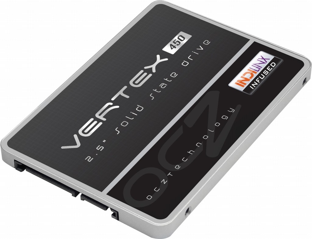
OCZ Launches the Vertex 450 Series Solid State Drives
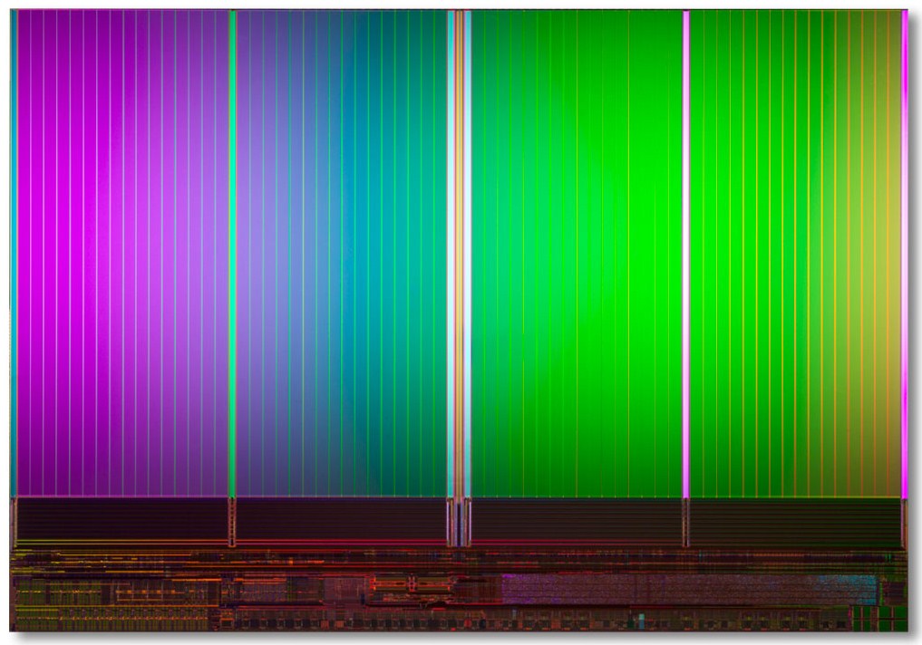
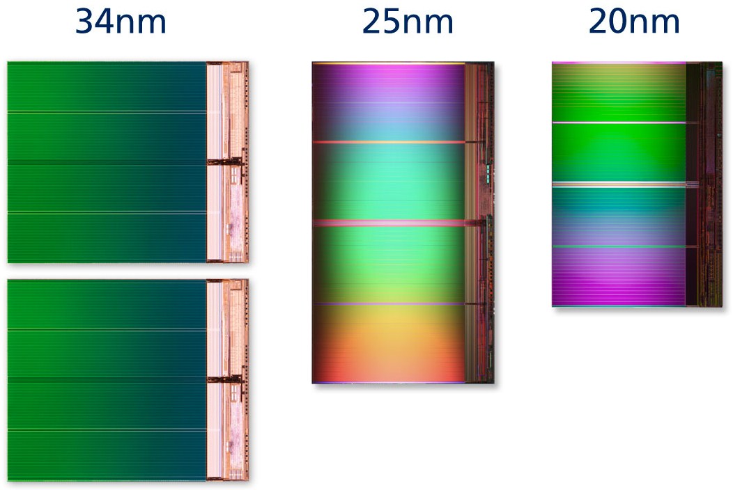
OCZ Technology Group, Inc., a leading provider of high-performance solid-state drives (SSDs) for computing devices and systems, today announced the release of the Vertex 450 SATA III SSD Series featuring the company's proprietary Indilinx Barefoot 3 M10 Series controller. As part of the leading-edge Vertex series, Vertex 450 lives up to its name and bridges the gap between high performance and mainstream solid-state storage. With advanced storage performance, reliability, and quality, the Vertex 450 utilizes 20 nm process geometry NAND flash to meet the needs of today's high-end consumer and client applications.
"As one of the industry's most highly awarded SSD Series to date, the Vertex name has become synonymous with the latest and greatest in flash-based storage providing an exceptional balance of performance and cost efficiency," said Daryl Lang, Senior Vice President of Product Management for OCZ Technology. "The Vertex 450 marks the first time this popular OCZ series utilizes in-house ASIC technology delivering an even greater level of speed, reliability and value for our customers."
"As one of the industry's most highly awarded SSD Series to date, the Vertex name has become synonymous with the latest and greatest in flash-based storage providing an exceptional balance of performance and cost efficiency," said Daryl Lang, Senior Vice President of Product Management for OCZ Technology. "The Vertex 450 marks the first time this popular OCZ series utilizes in-house ASIC technology delivering an even greater level of speed, reliability and value for our customers."