AMD Files Patent for Chiplet Machine Learning Accelerator to be Paired With GPU, Cache Chiplets
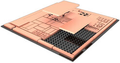
AMD has filed a patent whereby they describe a MLA (Machine Learning Accelerator) chiplet design that can then be paired with a GPU unit (such as RDNA 3) and a cache unit (likely a GPU-excised version of AMD's Infinity Cache design debuted with RDNA 2) to create what AMD is calling an "APD" (Accelerated Processing Device). The design would thus enable AMD to create a chiplet-based machine learning accelerator whose sole function would be to accelerate machine learning - specifically, matrix multiplication. This would enable capabilities not unlike those available through NVIDIA's Tensor cores.
This could give AMD a modular way to add machine-learning capabilities to several of their designs through the inclusion of such a chiplet, and might be AMD's way of achieving hardware acceleration of a DLSS-like feature. This would avoid the shortcomings associated with implementing it in the GPU package itself - an increase in overall die area, with thus increased cost and reduced yields, while at the same time enabling AMD to deploy it in other products other than GPU packages. The patent describes the possibility of different manufacturing technologies being employed in the chiplet-based design - harkening back to the I/O modules in Ryzen CPUs, manufactured via a 12 nm process, and not the 7 nm one used for the core chiplets. The patent also describes acceleration of cache-requests from the GPU die to the cache chiplet, and on-the-fly usage of it as actual cache, or as directly-addressable memory.
This could give AMD a modular way to add machine-learning capabilities to several of their designs through the inclusion of such a chiplet, and might be AMD's way of achieving hardware acceleration of a DLSS-like feature. This would avoid the shortcomings associated with implementing it in the GPU package itself - an increase in overall die area, with thus increased cost and reduced yields, while at the same time enabling AMD to deploy it in other products other than GPU packages. The patent describes the possibility of different manufacturing technologies being employed in the chiplet-based design - harkening back to the I/O modules in Ryzen CPUs, manufactured via a 12 nm process, and not the 7 nm one used for the core chiplets. The patent also describes acceleration of cache-requests from the GPU die to the cache chiplet, and on-the-fly usage of it as actual cache, or as directly-addressable memory.
