Apr 18th, 2025 15:34 EDT
change timezone
Latest GPU Drivers
New Forum Posts
- Can Intel recover in DYI market anytime soon? (9)
- Place your bets, what node will rtx 6000/RDNA 5(UDNA 1?) use (7)
- GPU Pricing and Performance (15)
- What are you playing? (23396)
- TPU's Nostalgic Hardware Club (20256)
- Spoofer Modified SMBIOS/BIOS – Need Help Restoring Original Motherboard Info (TUF GAMING B550-PLUS WiFi II) (2)
- Tried installing 576.02 - installer window disappears (20)
- RX 9000 series GPU Owners Club (392)
- GPU Database (300)
- Drives fail to work with Rufus Windows TO GO (2)
Popular Reviews
- ASUS GeForce RTX 5060 Ti TUF OC 16 GB Review
- NVIDIA GeForce RTX 5060 Ti PCI-Express x8 Scaling
- Palit GeForce RTX 5060 Ti Infinity 3 16 GB Review
- G.SKILL Trident Z5 NEO RGB DDR5-6000 32 GB CL26 Review - AMD EXPO
- ASUS GeForce RTX 5060 Ti Prime OC 16 GB Review
- Teevolution Terra Pro Review
- MSI GeForce RTX 5060 Ti Gaming OC 16 GB Review
- Zotac GeForce RTX 5060 Ti AMP 16 GB Review
- MSI GeForce RTX 5060 Ti Gaming Trio OC 16 GB Review
- ASUS GeForce RTX 5080 TUF OC Review
Controversial News Posts
- NVIDIA GeForce RTX 5060 Ti 16 GB SKU Likely Launching at $499, According to Supply Chain Leak (182)
- NVIDIA Sends MSRP Numbers to Partners: GeForce RTX 5060 Ti 8 GB at $379, RTX 5060 Ti 16 GB at $429 (127)
- Nintendo Confirms That Switch 2 Joy-Cons Will Not Utilize Hall Effect Stick Technology (105)
- Over 200,000 Sold Radeon RX 9070 and RX 9070 XT GPUs? AMD Says No Number was Given (100)
- Nintendo Switch 2 Launches June 5 at $449.99 with New Hardware and Games (99)
- NVIDIA Launches GeForce RTX 5060 Series, Beginning with RTX 5060 Ti This Week (98)
- Sony Increases the PS5 Pricing in EMEA and ANZ by Around 25 Percent (85)
- NVIDIA PhysX and Flow Made Fully Open-Source (77)
News Posts matching #CCD
Return to Keyword Browsing
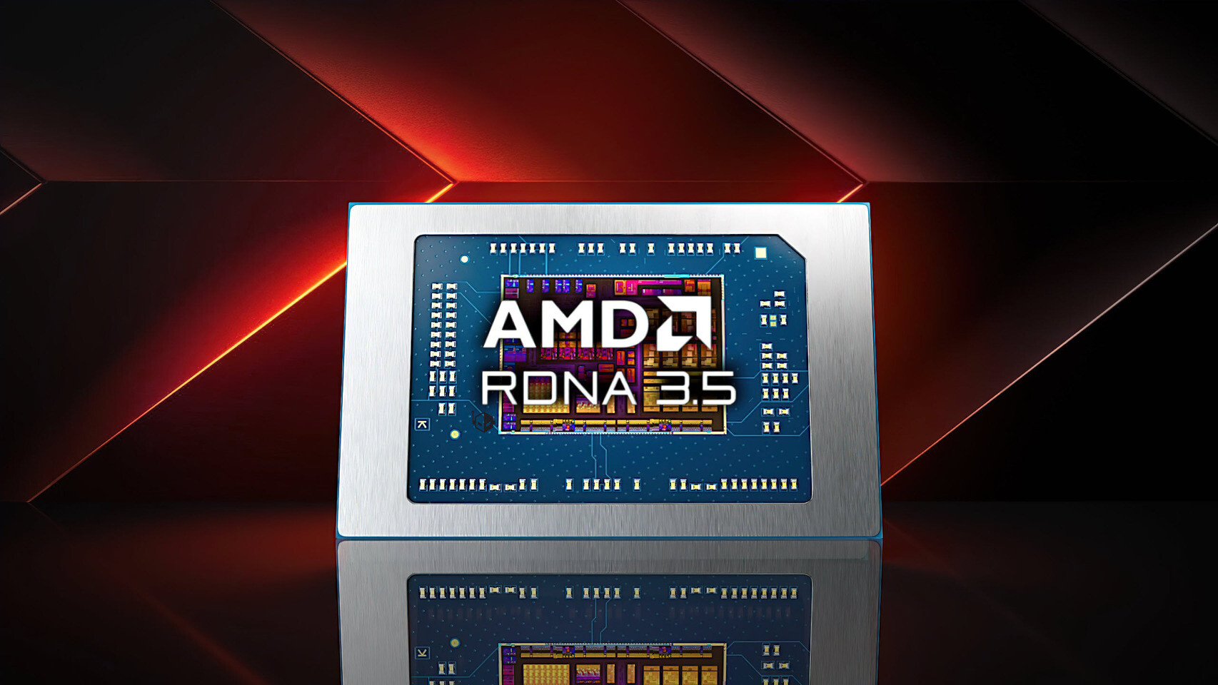
AMD Ryzen AI "Medusa Point" APU Could Arrive with Larger Footprint - BGA "FP10" Dimensions Leaked
Shipping manifests have served as fairly reliable sources of pre-launch information—Everest (aka Olrak29) has discovered many juicy details in recent times. Their latest sleuthing session—combing through NBD documents—has indicated AMD's (alleged) prepping of a larger socket design for next-generation mobile processors. A leaked document alludes to the existence of various "MEDUSA01" jig and block "FP10" socket validation parts. Current-generation Ryzen AI "Strix Point" 300 series APUs utilize the FP8 socket format. Based on the "MEDUSA01" shipping manifest, it seems that a successor will arrive with a larger footprint—measurements of 25 mm x 42.5 mm are repeated throughout the leaked description list. Industry watchdogs surmise that "Medusa Point's" BGA FP10 socket will be approximately 6% larger than its predecessor.
Mid-way through last month, insider theorizations pointed to "Medusa Point" being a chiplet-based design. A "single 12-core Zen 6 CCD" was linked to a TSMC 3 nm-class node, with "N4P" reportedly selected for a separate mobile client I/O die. Readily available 4 nm Ryzen AI "Strix Point" processors are monolithic in nature. Initial inside track info mentioned RDNA 4 technology in the same equation as "Medusa Point," but recent Team Red's recent-ish targeting of "GFX1153" places RDNA 3.5 as the de facto choice.

Mid-way through last month, insider theorizations pointed to "Medusa Point" being a chiplet-based design. A "single 12-core Zen 6 CCD" was linked to a TSMC 3 nm-class node, with "N4P" reportedly selected for a separate mobile client I/O die. Readily available 4 nm Ryzen AI "Strix Point" processors are monolithic in nature. Initial inside track info mentioned RDNA 4 technology in the same equation as "Medusa Point," but recent Team Red's recent-ish targeting of "GFX1153" places RDNA 3.5 as the de facto choice.


AMD "Medusa Point" APU with Zen 6 Confirmed to Use RDNA 3.5, RDNA 4 Reserved for Discrete GPUs
AMD's next-generation Zen 6-based "Medusa Point" mobile APUs will not feature RDNA 4 graphics as previously speculated, according to recent code discoveries in AMD GPUOpen Drivers on GitHub. The Device ID "GfxIp12" associated with RDNA 4 architecture has been reserved only for discrete GPUs, confirming that the current Radeon RX 9000 series will exclusively implement AMD's latest graphics architecture. Current technical documentation indicates AMD will instead extend RDNA 3.5 implementation beyond the Zen 5 portfolio while potentially positioning UDNA as the successor technology for integrated graphics.
The chiplet-based Medusa Point design will reportedly pair a single 12-core Zen 6 CCD manufactured on TSMC's 3 nm-class node with a mobile client I/O die likely built on N4P. This arrangement is significantly different from current monolithic mobile solutions. Earlier speculation indicates the Medusa Point platform may support 3D V-Cache variants, leveraging the same vertical stacking methodology employed in current Zen 5 implementations. The mobile processor's memory controllers and neural processing unit are expected to receive substantial updates. However, compatibility limitations with AMD's latest graphics features, like FSR 4 technology, remain a concern due to the absence of RDNA 4 silicon. The Zen 6-powered Medusa Point processor family is scheduled for release in 2026, targeting premium mobile computing applications with a performance profile that builds upon AMD's current Strix Halo positioning.
The chiplet-based Medusa Point design will reportedly pair a single 12-core Zen 6 CCD manufactured on TSMC's 3 nm-class node with a mobile client I/O die likely built on N4P. This arrangement is significantly different from current monolithic mobile solutions. Earlier speculation indicates the Medusa Point platform may support 3D V-Cache variants, leveraging the same vertical stacking methodology employed in current Zen 5 implementations. The mobile processor's memory controllers and neural processing unit are expected to receive substantial updates. However, compatibility limitations with AMD's latest graphics features, like FSR 4 technology, remain a concern due to the absence of RDNA 4 silicon. The Zen 6-powered Medusa Point processor family is scheduled for release in 2026, targeting premium mobile computing applications with a performance profile that builds upon AMD's current Strix Halo positioning.

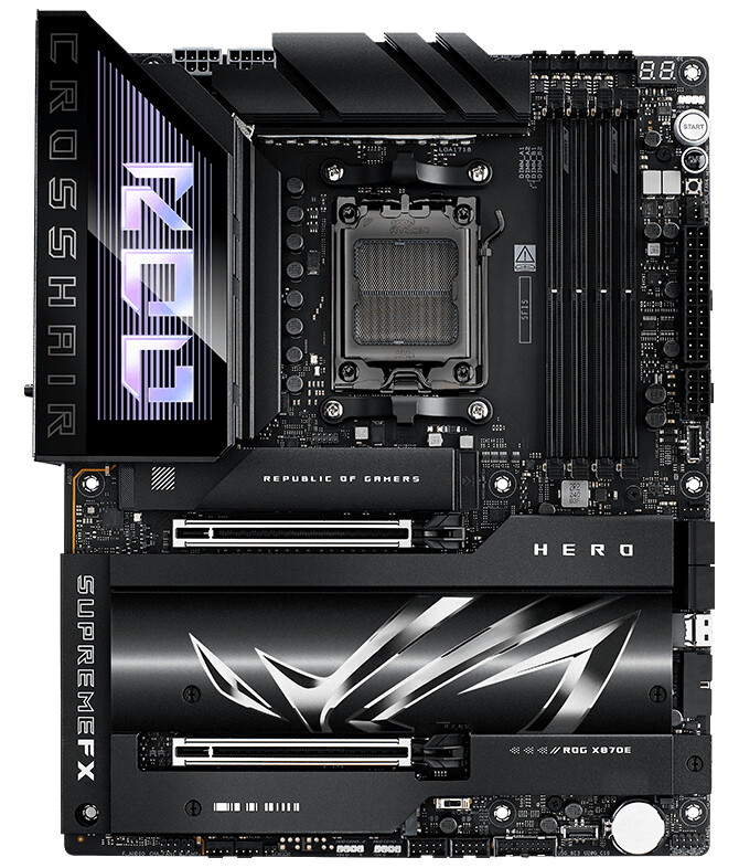
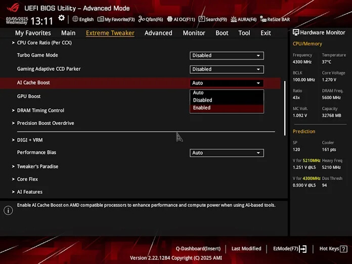
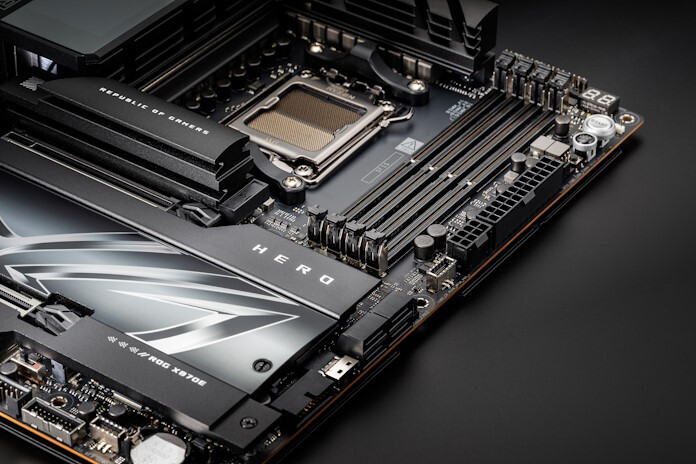
ASUS Introduces New "AI Cache Boost" BIOS Feature - R&D Team Claims Performance Uplift
Large language models (LLMs) love large quantities of memory—so much so, in fact, that AI enthusiasts are turning to multi-GPU setups to make even more VRAM available for their AI apps. But since many current LLMs are extremely large, even this approach has its limits. At times, the GPU will decide to make use of CPU processing power for this data, and when it does, the performance of your CPU cache and DRAM comes into play. All this means that when it comes to the performance of AI applications, it's not just the GPU that matters, but the entire pathway that connects the GPU to the CPU to the I/O die to the DRAM modules. It stands to reason, then, that there are opportunities to boost AI performance by optimizing these elements.
That's exactly what we've found as we've spent time in our R&D labs with the latest AMD Ryzen CPUs. AMD just launched two new Ryzen CPUs with AMD 3D V-Cache Technology, the AMD Ryzen 9 9950X3D and Ryzen 9 9900X3D, pushing the series into new performance territory. After testing a wide range of optimizations in a variety of workloads, we uncovered a range of settings that offer tangible benefits for AI enthusiasts. Now, we're ready to share these optimizations with you through a new BIOS feature: AI Cache Boost. Available through an ASUS AMD 800 Series motherboard and our most recent firmware update, AI Cache Boost can accelerate performance up to 12.75% when you're working with massive LLMs.


That's exactly what we've found as we've spent time in our R&D labs with the latest AMD Ryzen CPUs. AMD just launched two new Ryzen CPUs with AMD 3D V-Cache Technology, the AMD Ryzen 9 9950X3D and Ryzen 9 9900X3D, pushing the series into new performance territory. After testing a wide range of optimizations in a variety of workloads, we uncovered a range of settings that offer tangible benefits for AI enthusiasts. Now, we're ready to share these optimizations with you through a new BIOS feature: AI Cache Boost. Available through an ASUS AMD 800 Series motherboard and our most recent firmware update, AI Cache Boost can accelerate performance up to 12.75% when you're working with massive LLMs.
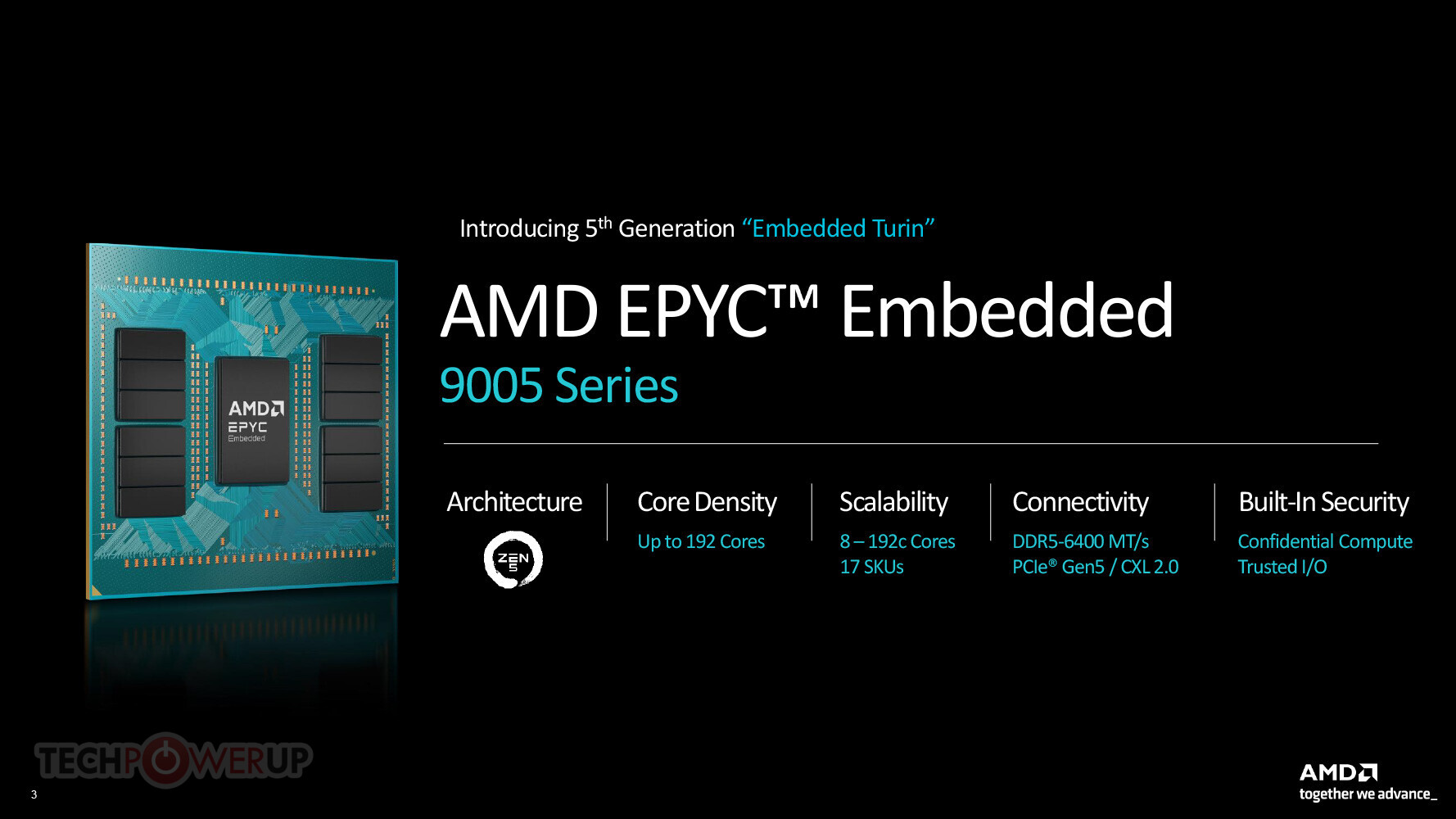
AMD Launches the EPYC Embedded 9005 "Turin" Family of Server Processors
AMD today launched the EPYC Embedded 9005 line of server processors in the embedded form-factor. These are non-socketed variants of the EPYC 9005 "Turin" server processors. The chips are intended for servers and other enterprise applications where processor replacements or upgradability are not a consideration. The EPYC Embedded 9005 "Turin" are otherwise every bit similar to the regular socketed EPYC 9005 series. These chips are based on a BGA version of the "Turin" chiplet-based processor, and powered by the "Zen 5" microarchitecture. Besides the BGA package, the EPYC Embedded 9005 series comes with a few features relevant to its form-factor and target use-cases.
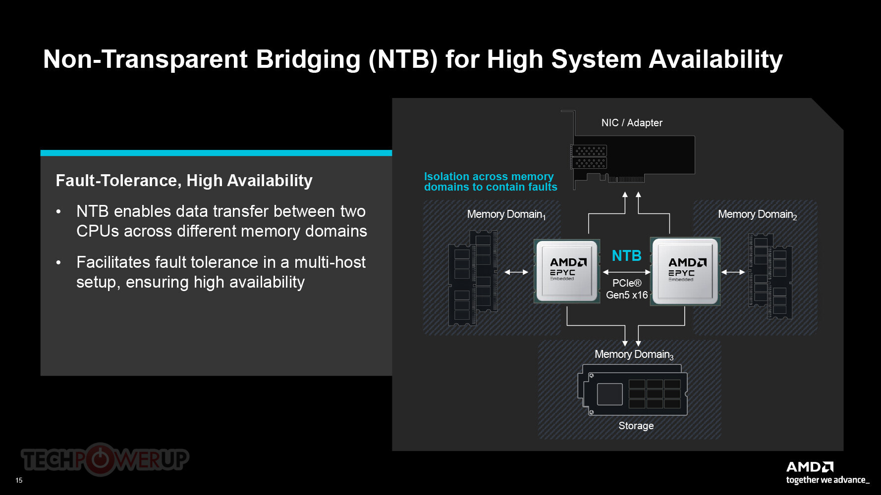
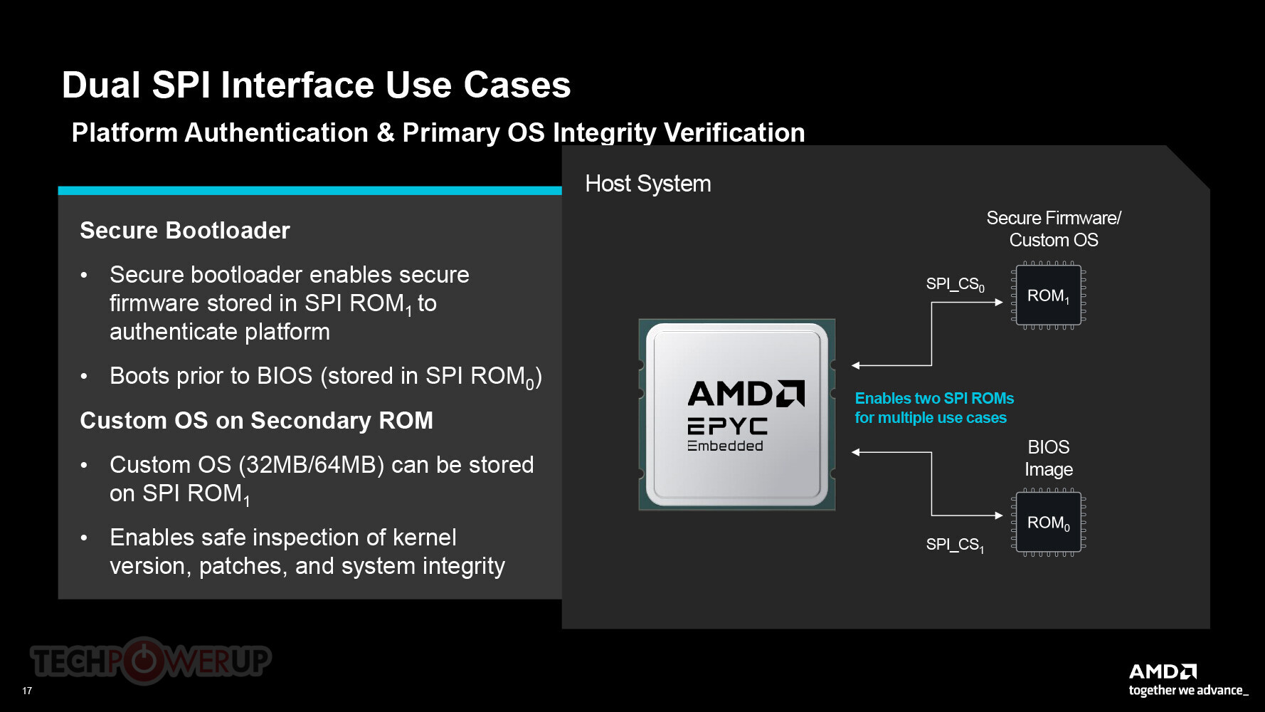
To begin with, the EPYC Embedded 9005 "Turin" series comes with NTB (non-transparent bridging), a technology that enables high-performance data transfer between two processor packages across different memory domains. NTB doesn't use Infinity Fabric or even CXL, but a regular PCI-Express 5.0 x16 connection. It isn't intended to provide cache coherence, but to absorb faults across various memory domains. Next up, the series supports DRAM flush for enhanced power-loss mitigation. Upon detecting a power loss, the processor immediately dumps memory onto NVMe storage, before the machine turns off. On restart, the BIOS copies this memory dump from the NVMe SSD back to DRAM. Thirdly, the processors in the series support dual SPI flash interfaces, which enables system architects to embed lightweight operating systems directly onto a 64 MB SPI flash ROM, besides the primary SPI flash that stores the system BIOS. This lightweight OS can act like a bootloader for operating systems in other local storage devices.


To begin with, the EPYC Embedded 9005 "Turin" series comes with NTB (non-transparent bridging), a technology that enables high-performance data transfer between two processor packages across different memory domains. NTB doesn't use Infinity Fabric or even CXL, but a regular PCI-Express 5.0 x16 connection. It isn't intended to provide cache coherence, but to absorb faults across various memory domains. Next up, the series supports DRAM flush for enhanced power-loss mitigation. Upon detecting a power loss, the processor immediately dumps memory onto NVMe storage, before the machine turns off. On restart, the BIOS copies this memory dump from the NVMe SSD back to DRAM. Thirdly, the processors in the series support dual SPI flash interfaces, which enables system architects to embed lightweight operating systems directly onto a 64 MB SPI flash ROM, besides the primary SPI flash that stores the system BIOS. This lightweight OS can act like a bootloader for operating systems in other local storage devices.

AMD Ryzen AI Max+ "Strix Halo" Die Exposed and Annotated
AMD's "Strix Halo" APU, marketed as Ryzen AI Max+, has just been exposed in die-shot analysis. Confirming the processor's triple-die architecture, the package showcases a total silicon footprint of 441.72 mm² that integrates advanced CPU, GPU, and AI acceleration capabilities within a single package. The processor's architecture centers on two 67.07 mm² CPU CCDs, each housing eight Zen 5 cores with a dedicated 8 MB L2 cache. A substantial 307.58 mm² I/O complements these die that houses an RDNA 3.5-based integrated GPU featuring 40 CUs and AMD's XDNA 2 NPU. The memory subsystem demonstrates a 256-bit LPDDR5X interface capable of delivering 256 GB/s bandwidth, supported by 32 MB of strategically placed Last Level Cache to optimize data throughput.
The die shots reveal notable optimizations for mobile deployment, including shortened die-to-die interfaces that reduce the interconnect distance by 2 mm compared to desktop implementations. Some through-silicon via structures are present, which suggest potential compatibility with AMD's 3D V-Cache technology, though the company has not officially confirmed plans for such implementations. The I/O die integrates comprehensive connectivity options, including PCIe 4.0 x16 lanes and USB4 support, while also housing dedicated media engines with full AV1 codec support. Initial deployments of the Strix Halo APU will commence with the ASUS ROG Flow Z13 launch on February 25, marking the beginning of what AMD anticipates will be broad adoption across premium mobile computing platforms.


The die shots reveal notable optimizations for mobile deployment, including shortened die-to-die interfaces that reduce the interconnect distance by 2 mm compared to desktop implementations. Some through-silicon via structures are present, which suggest potential compatibility with AMD's 3D V-Cache technology, though the company has not officially confirmed plans for such implementations. The I/O die integrates comprehensive connectivity options, including PCIe 4.0 x16 lanes and USB4 support, while also housing dedicated media engines with full AV1 codec support. Initial deployments of the Strix Halo APU will commence with the ASUS ROG Flow Z13 launch on February 25, marking the beginning of what AMD anticipates will be broad adoption across premium mobile computing platforms.


AMD Zen 6 Powers "Medusa Point" Mobile and "Olympic Ridge" Desktop Processors
AMD is readying two important client segment processors powered by the next-generation "Zen 6" microarchitecture, according to a sensational new report by Moore's Law is Dead. These are the "Medusa Point" mobile processor, and the "Olympic Ridge" desktop. The former is a BGA roughly the size and Z-Height of the current "Strix Point," but the latter is being designed for the existing Socket AM5, making it the third (and probably final) microarchitecture to do so. If you recall, Socket AM4 served three generations of Zen, not counting the refreshed "Zen+." At the heart of the effort is a new CPU complex die (CCD) that AMD plans to use across its client and server lineup.
The "Zen 6" performance CCD is being designed for a 3 nm-class node, likely the TSMC N3E. This node promises a significant increase in transistor density, power, and clock speed improvements over the current TSMC N4P node being used to build the "Zen 5" CCD. Here's where it gets interesting. The CCD contains twelve full-sized "Zen 6" cores, marking the first increase in core-counts of AMD's performance cores since its very first "Zen" CCD. All 12 of these cores are part of a single CPU core complex (CCX), and share a common L3 cache. There could be a proportionate increase in cache size to 48 MB. AMD is also expected to improve the way the CCDs communicate with the I/O die and among each other.


The "Zen 6" performance CCD is being designed for a 3 nm-class node, likely the TSMC N3E. This node promises a significant increase in transistor density, power, and clock speed improvements over the current TSMC N4P node being used to build the "Zen 5" CCD. Here's where it gets interesting. The CCD contains twelve full-sized "Zen 6" cores, marking the first increase in core-counts of AMD's performance cores since its very first "Zen" CCD. All 12 of these cores are part of a single CPU core complex (CCX), and share a common L3 cache. There could be a proportionate increase in cache size to 48 MB. AMD is also expected to improve the way the CCDs communicate with the I/O die and among each other.


AMD to Build Next-Gen I/O Dies on Samsung 4nm, Not TSMC N4P
Back in January, we covered a report about AMD designing its next-generation "Zen 6" CCDs on a 3 nm-class node by TSMC, and developing a new line of server and client I/O dies (cIOD and sIOD). The I/O die is a crucial piece of silicon that contains all the uncore components of the processor, including the memory controllers, the PCIe root complex, and Infinity Fabric interconnects to the CCDs and multi-socket connections. Back then it was reported that these new-generation I/O dies were being designed on the 4 nm silicon fabrication process, which was interpreted as being AMD's favorite 4 nm-class node, the TSMC N4P, on which the company builds everything from its current "Strix Point" mobile processors to the "Zen 5" CCDs. It turns out that AMD has other plans, and is exploring a 4 nm-class node by Samsung.
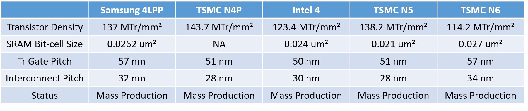
This node is very likely the Samsung 4LPP, also known as the SF4, which has been in mass-production since 2022. The table below shows how the SF4 compares with TSMC N4P and Intel 4, where it is shown striking a balance between the two. We have also added values for the TSMC N5 node from which the N4P is derived from, and you can see that the SF4 offers comparable transistor density to the N5, and is a significant improvement in transistor density over the TSMC N6, which AMD uses for its current generation of sIOD and cIOD. The new 4 nm node will allow AMD to reduce the TDP of the I/O die, implement a new power management solution, and more importantly, the need for a new I/O die is driven by the need for updated memory controllers that support higher DDR5 speeds and compatibility with new kinds of DIMMs, such as CUDIMMs, RDIMMs with RCDs, etc.
This node is very likely the Samsung 4LPP, also known as the SF4, which has been in mass-production since 2022. The table below shows how the SF4 compares with TSMC N4P and Intel 4, where it is shown striking a balance between the two. We have also added values for the TSMC N5 node from which the N4P is derived from, and you can see that the SF4 offers comparable transistor density to the N5, and is a significant improvement in transistor density over the TSMC N6, which AMD uses for its current generation of sIOD and cIOD. The new 4 nm node will allow AMD to reduce the TDP of the I/O die, implement a new power management solution, and more importantly, the need for a new I/O die is driven by the need for updated memory controllers that support higher DDR5 speeds and compatibility with new kinds of DIMMs, such as CUDIMMs, RDIMMs with RCDs, etc.
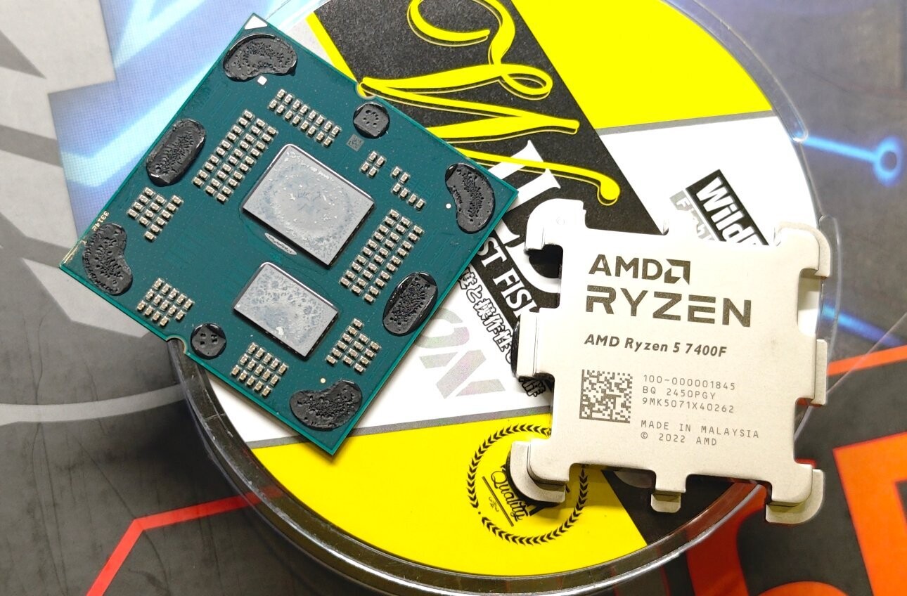
AMD Ryzen 5 7400F De-Lid Reveals Thermal Paste Instead of STIM
Priced at the equivalent of $116, the China-exclusive Ryzen 5 7400F is a 6-core/12-thread processor powered by the older "Zen 4" microarchitecture, but which is based on the "Raphael" MCM, giving it a comprehensive PCIe Gen 5 I/O (as opposed to designing such a chip based on the "Phoenix Point" monolithic silicon with its PCIe Gen 4 I/O). The chip benefits from the full 32 MB on-die L3 cache being enabled on the "Zen 4" CCD, besides the full 1 MB per core L2 cache, and that I/O, but misses out on the iGPU. At its price, the 7400F is attracting a segment of value-conscious gamers.
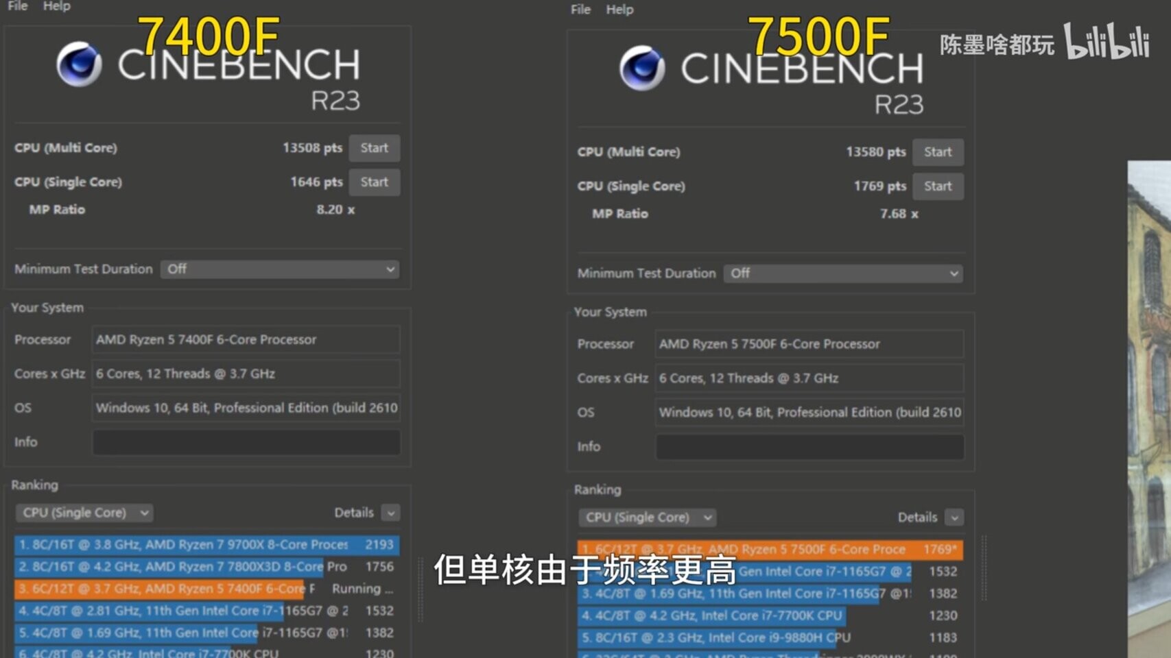
To bring this chip at its price point, AMD had to cut costs somewhere, and Chinese PC enthusiast "Melon Master" soon found out where. On de-lidding (removing IHS) of the Ryzen 5 7400F, it was found that the chip does not use a soldered TIM like the other Ryzen 7000 series "Raphael" processors, instead using more cost-effective thermal paste, as is common in entry-level chips from both AMD and Intel. Harukaze5719 comments that this could be the reason the chip has a fairly noticeable Cinebench R23 performance delta against the Ryzen 5 7500F that's globally available, and has STIM, but is priced at $145. The 7400F and 7500F share the same base frequency of 3.70 GHz, but while the former boosts up to 4.70 GHz, the latter goes all the way up to 5.00 GHz.

To bring this chip at its price point, AMD had to cut costs somewhere, and Chinese PC enthusiast "Melon Master" soon found out where. On de-lidding (removing IHS) of the Ryzen 5 7400F, it was found that the chip does not use a soldered TIM like the other Ryzen 7000 series "Raphael" processors, instead using more cost-effective thermal paste, as is common in entry-level chips from both AMD and Intel. Harukaze5719 comments that this could be the reason the chip has a fairly noticeable Cinebench R23 performance delta against the Ryzen 5 7500F that's globally available, and has STIM, but is priced at $145. The 7400F and 7500F share the same base frequency of 3.70 GHz, but while the former boosts up to 4.70 GHz, the latter goes all the way up to 5.00 GHz.
ASUS Readies NUC Mini PCs Powered by AMD Ryzen AI MAX "Strix Halo" SoCs
ASUS is working on a new line of NUC mini PCs powered by the AMD Ryzen AI MAX "Strix Halo" mobile processors that come with oversized iGPUs and CPU core counts as high as 16-core/32-thread "Zen 5." This was sniffed out in shipping manifests by Olrak29_ on its way to being tested by the BIS (Bureau of Indian Standards) for regulatory certification similar to CE, with the manifest describing the NUC model as the "NUC14LNS," meaning that this box is from the NUC 14 series. The manifest describes the NUC sample as featuring the top of the line Ryzen AI MAX+ 395.
The Ryzen AI MAX+ 395 maxes out everything on the silicon, featuring 16 "Zen 5" CPU cores across two CCDs with full 512-bit FPUs, with 80 MB of "total cache" (L3+L2) between them; a 50 TOPS-class NPU that can locally accelerate Microsoft Copilot+, and that large RDNA 3.5 iGPU with 40 compute units (2,560 stream processors), 80 AI accelerators, and 40 ray accelerators. What's interesting about this NUC is that it will not come with SO-DIMM slots, since the "Strix Halo" SoC features a 256-bit wide LPDDR5X memory interface. It will either have hardwired memory, or use a pair of LPCAMM2 modules (each with a 128-bit bus width), which is less likely. With all the rage about AI developers using M4-powered Mac minis to accelerate DeepSeek, is ASUS eying a slice of the AI market?

The Ryzen AI MAX+ 395 maxes out everything on the silicon, featuring 16 "Zen 5" CPU cores across two CCDs with full 512-bit FPUs, with 80 MB of "total cache" (L3+L2) between them; a 50 TOPS-class NPU that can locally accelerate Microsoft Copilot+, and that large RDNA 3.5 iGPU with 40 compute units (2,560 stream processors), 80 AI accelerators, and 40 ray accelerators. What's interesting about this NUC is that it will not come with SO-DIMM slots, since the "Strix Halo" SoC features a 256-bit wide LPDDR5X memory interface. It will either have hardwired memory, or use a pair of LPCAMM2 modules (each with a 128-bit bus width), which is less likely. With all the rage about AI developers using M4-powered Mac minis to accelerate DeepSeek, is ASUS eying a slice of the AI market?


AMD Ryzen Threadripper 9000 "Shimada Peak" 64-Core & 32-Core SKUs Leak Out
Unannounced AMD Threadripper 9000 "Shimada Peak" processor SKUs have once again appeared on leaked shipping manifests—a 96-core variant was uncovered under similar circumstances last summer. The latest discovery—courtesy of reliable investigator Everest/Olrak_29 combing through info published on NBD—reveals a Zen 5-based product stack that lists 16, 32, 64 and 96-core models. Until now, industry watchdogs have not spotted evidence of 32-core and 64-core SKUs—alongside prior leaks that only mentioned 16-core and 96-core parts.
Team Red has not officially announced that it is working on a follow-up to its current generation Zen 4-equipped Threadripper 7000 "Storm Peak" CPU series, but tipsters believe that fundamental similarities—based on leaked core counts and specifications—position "Shimada Peak" as the logical/inevitable successor. Speculation points to all the leaked Threadripper 9000 HEDT processors having a TDP rating of 350 W. Industry insiders propose that the highest-end variant—sporting 96 cores and 192 threads—will contain 12 CCDs (eight cores per CCD), 32 MB L3 cache (per CCD), and a lone I/O die. Wccftech theorizes that the 32-core model will be specced with four CCDs, while "the 64-core variant will come with eight CCDs." Insiders have whispered about a possible "later in 2025" launch window for "Shimada Peak."

Team Red has not officially announced that it is working on a follow-up to its current generation Zen 4-equipped Threadripper 7000 "Storm Peak" CPU series, but tipsters believe that fundamental similarities—based on leaked core counts and specifications—position "Shimada Peak" as the logical/inevitable successor. Speculation points to all the leaked Threadripper 9000 HEDT processors having a TDP rating of 350 W. Industry insiders propose that the highest-end variant—sporting 96 cores and 192 threads—will contain 12 CCDs (eight cores per CCD), 32 MB L3 cache (per CCD), and a lone I/O die. Wccftech theorizes that the 32-core model will be specced with four CCDs, while "the 64-core variant will come with eight CCDs." Insiders have whispered about a possible "later in 2025" launch window for "Shimada Peak."


AMD to Build Zen 6 CCD on TSMC 3nm Process, Next-Gen cIOD and sIOD on 4nm
AMD is rumored to be building its next-generation CCD (core complex die) that implements the "Zen 6" microarchitecture, on the 3 nm TSMC N3E foundry node. This is part of a set of rumors from ChipHell forum, which got past rumors on AMD right. Apparently, AMD will also refresh the I/O dies for its next generation process, building them on the 4 nm foundry node, likely the TSMC N4C. The TSMC N3E node offers a 20% speed improvement, over 30% power savings, and approximately 60% logic density increase over TSMC N5, whereas the TSMC N4P node that the company uses for its current "Zen 5" chiplets only clock minor increases in logic density and power over N5. The N3E node relies on EUV double-patterning to achieve its logic density increases.
Perhaps the most interesting piece of news is the new-generation I/O dies. AMD is building these on the 4 nm node, which is a significant step up from the 6 nm node its current I/O dies are built on. On the client side of things, 4 nm will enable AMD to give the new cIOD an updated iGPU, probably based on a newer graphics architecture, such as RDNA 3.5. It will also give AMD the opportunity to integrate an NPU. The company might also update its key I/O components, such as the DDR5 memory controllers, to support higher memory speeds unlocked by CUDIMMs. We don't predict any updates on the PCIe front, since AMD is expected to carry on with Socket AM5, which determines that the cIOD puts out 28 PCIe Gen 5 lanes. At best, the USB interface put out from the processor could be updated to USB4 through an on-die host controller. Over on the server side, the new-generation sIOD will bring much needed increases to the DDR5 memory speeds enabled by clock drivers.
Perhaps the most interesting piece of news is the new-generation I/O dies. AMD is building these on the 4 nm node, which is a significant step up from the 6 nm node its current I/O dies are built on. On the client side of things, 4 nm will enable AMD to give the new cIOD an updated iGPU, probably based on a newer graphics architecture, such as RDNA 3.5. It will also give AMD the opportunity to integrate an NPU. The company might also update its key I/O components, such as the DDR5 memory controllers, to support higher memory speeds unlocked by CUDIMMs. We don't predict any updates on the PCIe front, since AMD is expected to carry on with Socket AM5, which determines that the cIOD puts out 28 PCIe Gen 5 lanes. At best, the USB interface put out from the processor could be updated to USB4 through an on-die host controller. Over on the server side, the new-generation sIOD will bring much needed increases to the DDR5 memory speeds enabled by clock drivers.
AMD Implements New CCD Connection in "Strix Halo" Ryzen AI Max Processors
Thanks to the informative breakdown by Chips and Cheese, we are learning that AMD's latest Ryzen AI processors for laptops, codenamed "Strix Halo," utilize a parallel "sea of wires" interconnect system between their chiplets, replacing the SERDES (serializer/deserializer) approach found in desktop Ryzen models. The processor's physical implementation consists of two Core Complex Dies (CCDs), each manufactured on TSMC's N4 (4 nm) process and containing up to eight Zen 5 cores with full 512-bit floating point units. Notably, the I/O die (IOD) is also produced using the N4 process, marking an advancement from the N6 (6 nm) process used in standard Ryzen IODs on desktops. The key change lies in the inter-chiplet communication system. While the Ryzen 9000 series (Granite Ridge) employs SERDES to convert parallel data to serial for transmission between chiplets, Strix Halo implements direct parallel data transmission through multiple physical connections.
This design achieves 32 bytes per clock cycle throughput and eliminates the latency overhead associated with serialization/deserialization processes. The parallel interconnect architecture also removes the need for connection retraining during power state transitions, a limitation present in SERDES implementations. However, this design choice necessitates additional substrate complexity due to increased connection density and requires more pins for external connections, suggesting possible modifications to the CCD design compared to desktop variants. AMD's implementation required more complex substrate manufacturing processes to accommodate the dense parallel connections between chiplets. The decision to prioritize this more challenging design approach was driven by requirements for lower latency and power consumption in data-intensive workloads, where consistent high-bandwidth communication between chiplets is crucial.
This design achieves 32 bytes per clock cycle throughput and eliminates the latency overhead associated with serialization/deserialization processes. The parallel interconnect architecture also removes the need for connection retraining during power state transitions, a limitation present in SERDES implementations. However, this design choice necessitates additional substrate complexity due to increased connection density and requires more pins for external connections, suggesting possible modifications to the CCD design compared to desktop variants. AMD's implementation required more complex substrate manufacturing processes to accommodate the dense parallel connections between chiplets. The decision to prioritize this more challenging design approach was driven by requirements for lower latency and power consumption in data-intensive workloads, where consistent high-bandwidth communication between chiplets is crucial.

Apr 18th, 2025 15:34 EDT
change timezone
Latest GPU Drivers
New Forum Posts
- Can Intel recover in DYI market anytime soon? (9)
- Place your bets, what node will rtx 6000/RDNA 5(UDNA 1?) use (7)
- GPU Pricing and Performance (15)
- What are you playing? (23396)
- TPU's Nostalgic Hardware Club (20256)
- Spoofer Modified SMBIOS/BIOS – Need Help Restoring Original Motherboard Info (TUF GAMING B550-PLUS WiFi II) (2)
- Tried installing 576.02 - installer window disappears (20)
- RX 9000 series GPU Owners Club (392)
- GPU Database (300)
- Drives fail to work with Rufus Windows TO GO (2)
Popular Reviews
- ASUS GeForce RTX 5060 Ti TUF OC 16 GB Review
- NVIDIA GeForce RTX 5060 Ti PCI-Express x8 Scaling
- Palit GeForce RTX 5060 Ti Infinity 3 16 GB Review
- G.SKILL Trident Z5 NEO RGB DDR5-6000 32 GB CL26 Review - AMD EXPO
- ASUS GeForce RTX 5060 Ti Prime OC 16 GB Review
- Teevolution Terra Pro Review
- MSI GeForce RTX 5060 Ti Gaming OC 16 GB Review
- Zotac GeForce RTX 5060 Ti AMP 16 GB Review
- MSI GeForce RTX 5060 Ti Gaming Trio OC 16 GB Review
- ASUS GeForce RTX 5080 TUF OC Review
Controversial News Posts
- NVIDIA GeForce RTX 5060 Ti 16 GB SKU Likely Launching at $499, According to Supply Chain Leak (182)
- NVIDIA Sends MSRP Numbers to Partners: GeForce RTX 5060 Ti 8 GB at $379, RTX 5060 Ti 16 GB at $429 (127)
- Nintendo Confirms That Switch 2 Joy-Cons Will Not Utilize Hall Effect Stick Technology (105)
- Over 200,000 Sold Radeon RX 9070 and RX 9070 XT GPUs? AMD Says No Number was Given (100)
- Nintendo Switch 2 Launches June 5 at $449.99 with New Hardware and Games (99)
- NVIDIA Launches GeForce RTX 5060 Series, Beginning with RTX 5060 Ti This Week (98)
- Sony Increases the PS5 Pricing in EMEA and ANZ by Around 25 Percent (85)
- NVIDIA PhysX and Flow Made Fully Open-Source (77)