Friday, February 14th 2025

AMD Zen 6 Powers "Medusa Point" Mobile and "Olympic Ridge" Desktop Processors
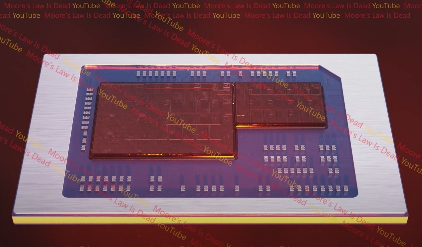
AMD is readying two important client segment processors powered by the next-generation "Zen 6" microarchitecture, according to a sensational new report by Moore's Law is Dead. These are the "Medusa Point" mobile processor, and the "Olympic Ridge" desktop. The former is a BGA roughly the size and Z-Height of the current "Strix Point," but the latter is being designed for the existing Socket AM5, making it the third (and probably final) microarchitecture to do so. If you recall, Socket AM4 served three generations of Zen, not counting the refreshed "Zen+." At the heart of the effort is a new CPU complex die (CCD) that AMD plans to use across its client and server lineup.
The "Zen 6" performance CCD is being designed for a 3 nm-class node, likely the TSMC N3E. This node promises a significant increase in transistor density, power, and clock speed improvements over the current TSMC N4P node being used to build the "Zen 5" CCD. Here's where it gets interesting. The CCD contains twelve full-sized "Zen 6" cores, marking the first increase in core-counts of AMD's performance cores since its very first "Zen" CCD. All 12 of these cores are part of a single CPU core complex (CCX), and share a common L3 cache. There could be a proportionate increase in cache size to 48 MB. AMD is also expected to improve the way the CCDs communicate with the I/O die and among each other.


 Going all the way back to the Ryzen 3000 series "Matisse," the two CCDs on the client desktop processor have had Infinity Fabric links to the I/O die, but no direct high-bandwidth interconnects between the two CCDs. For threads to migrate between cores of the two CCDs, they would have to make a round-trip through the main memory. AMD is looking to solve this with the introduction of a new low-latency bridge connection between the two CCDs. If the goal is to enable threads to seamlessly migrate among cores of the two CCDs, cutting out round-trips to the main memory, then the purpose of this bridge interconnect is to establish cache coherency between the two CCDs. This would vastly lower intercore latency.
Here's where things get very interesting. Apparently, the "Medusa Point" mobile processor is chiplet-based, and will use a single 12-core "Zen 6" chiplet, with a large mobile client I/O die built on an older node, likely the N4P. This mobile cIOD will contain an updated iGPU that's powered by the newer RDNA 4 graphics architecture. It will also contain the chip's memory controllers, and an updated NPU. We hope AMD works to increase the number of PCIe lanes put out by this I/O die, or at least update it to PCIe Gen 5. Pictures show small rectangular structures on the mobile client I/O die causing some speculation that it is some kind of low power island CCX with "Zen 6c" cores, although MLID lays this to rest by saying that these are workgroup processors (WGPs) of the iGPU. There are eight of these and a large slab of L2 cache, which seems to confirm that the iGPU is based on the RDNA 4 graphics architecture, and has 16 compute units (CU).
Since AMD is using the same CCD for "Medusa Point" as the "Olympic Ridge" desktop processor, you could expect variants of "Medusa Point" with 3D V-Cache. The 3D V-Cache technology is expected to be implemented on "Zen 6" much in the same way it is on "Zen 5," with an upside-down stacking—3D V-Cache die (L3D) below, with CCD on top.
Given the increase in CPU core counts, especially with "Olympic Ridge" getting up to 24 cores with two CCDs, and the inter-CCD bridge interconnect for cache coherency, AMD is going to need a new client I/O die for desktop. We've already discussed this in older articles. The new cIOD is expected to be built on the Samsung 4LPP (4 nm EUV) foundry node, which offers improvements over the TSMC N6 DUV node the current cIOD is being built on. A key area of focus for AMD will be the memory controllers, which will be updated to support higher DDR5 memory speeds using technologies such as CKD. You can currently run a "Granite Ridge" processor with memory speeds of up to DDR5-8000 but using a 1:2 clock divider is engaged between FCLK and MCLK, with 1:1 speeds being limited to around DDR5-6400. The new memory controllers will look to increase speeds with 1:1, and unlock speeds beyond 10000 MT/s with 1:2.
Then there's the matter of AI acceleration, and the new cIOD will present AMD with the opportunity to implement at least a 50 TOPS-class XDNA 2 NPU. Intel received flack for giving its "Arrow Lake" processors a 16 TOPS-class NPU that doesn't meet Copilot+ requirements, and the company is probably working to fix this in "Panther Lake," and so if AMD decides to implement an NPU on the cIOD for "Olympic Ridge," we predict it will be at least 50 TOPS-class.
Source:
Moore's Law is Dead
The "Zen 6" performance CCD is being designed for a 3 nm-class node, likely the TSMC N3E. This node promises a significant increase in transistor density, power, and clock speed improvements over the current TSMC N4P node being used to build the "Zen 5" CCD. Here's where it gets interesting. The CCD contains twelve full-sized "Zen 6" cores, marking the first increase in core-counts of AMD's performance cores since its very first "Zen" CCD. All 12 of these cores are part of a single CPU core complex (CCX), and share a common L3 cache. There could be a proportionate increase in cache size to 48 MB. AMD is also expected to improve the way the CCDs communicate with the I/O die and among each other.


Here's where things get very interesting. Apparently, the "Medusa Point" mobile processor is chiplet-based, and will use a single 12-core "Zen 6" chiplet, with a large mobile client I/O die built on an older node, likely the N4P. This mobile cIOD will contain an updated iGPU that's powered by the newer RDNA 4 graphics architecture. It will also contain the chip's memory controllers, and an updated NPU. We hope AMD works to increase the number of PCIe lanes put out by this I/O die, or at least update it to PCIe Gen 5. Pictures show small rectangular structures on the mobile client I/O die causing some speculation that it is some kind of low power island CCX with "Zen 6c" cores, although MLID lays this to rest by saying that these are workgroup processors (WGPs) of the iGPU. There are eight of these and a large slab of L2 cache, which seems to confirm that the iGPU is based on the RDNA 4 graphics architecture, and has 16 compute units (CU).
Since AMD is using the same CCD for "Medusa Point" as the "Olympic Ridge" desktop processor, you could expect variants of "Medusa Point" with 3D V-Cache. The 3D V-Cache technology is expected to be implemented on "Zen 6" much in the same way it is on "Zen 5," with an upside-down stacking—3D V-Cache die (L3D) below, with CCD on top.
Given the increase in CPU core counts, especially with "Olympic Ridge" getting up to 24 cores with two CCDs, and the inter-CCD bridge interconnect for cache coherency, AMD is going to need a new client I/O die for desktop. We've already discussed this in older articles. The new cIOD is expected to be built on the Samsung 4LPP (4 nm EUV) foundry node, which offers improvements over the TSMC N6 DUV node the current cIOD is being built on. A key area of focus for AMD will be the memory controllers, which will be updated to support higher DDR5 memory speeds using technologies such as CKD. You can currently run a "Granite Ridge" processor with memory speeds of up to DDR5-8000 but using a 1:2 clock divider is engaged between FCLK and MCLK, with 1:1 speeds being limited to around DDR5-6400. The new memory controllers will look to increase speeds with 1:1, and unlock speeds beyond 10000 MT/s with 1:2.
Then there's the matter of AI acceleration, and the new cIOD will present AMD with the opportunity to implement at least a 50 TOPS-class XDNA 2 NPU. Intel received flack for giving its "Arrow Lake" processors a 16 TOPS-class NPU that doesn't meet Copilot+ requirements, and the company is probably working to fix this in "Panther Lake," and so if AMD decides to implement an NPU on the cIOD for "Olympic Ridge," we predict it will be at least 50 TOPS-class.
91 Comments on AMD Zen 6 Powers "Medusa Point" Mobile and "Olympic Ridge" Desktop Processors
Ryzen 5 11600X 8 cores
Ryzen 7 11709X 12 cores
Ryzen 9 11900X 16 cores
Ryzen 9 11950X 24 cores
Maybe finally new Ryzen 3 with 6 cores?No chance, in the best case 4cu
*PCIe Gen 6 on-CPU? Gen5x4 link to chipset? -allowing for better Gen3 and Gen4 'fanout' from the Promontory.
Hey... I can dream? Right? :rolleyes:Agreed.
Truth be told, if there is enough bandwidth to not bottleneck performance on GPUs with mobile power envelope and embedded SSDs, I'd call it a win. PCIe 5.0 x4 for GPUs and x2 to x1 for SSDs may well be sufficient, cutting down on board footprint at the same time.
It would be a shame, especially for lower end peripherals without PCIe 5.0 support, of course.
----
Hopefully existing motherboards would support the new CPU without major limitations. Faster memory with CKD and without IF bottleneck would be so sweet.
*salute*
might as well fuck nvidia out of the bottom of the market by making igpu solutions good enough
Look at how speed drops as more threads are introduced on Zen 5. Applying logic of 3nm (1.328x xtors/1.164 clock) and you can pretty much come to the conclusion 12 cores (11 in use) is the way to go.
For instance, on a console, they'll probably reserve a core for the OS, which would make sense (hammer 11 cores/22 threads in games and leave one more-or-less idle).
WRT bw, current PS5pro: Something like 15000/3000mhz split, essentially same as a 6000mhz 128-bit desktop chip for CPU. If 32gbps (which next-gen consoles probably are) figure it out.
I've been saying it's probably ~60TF*. I doubt they would make it faster than 1440p where 9070xt is 1080p best/worse-case (depending on you look at it), so less than ~40% (38.8% to scale).
9070xt* has 20gbps, so the obvious thing to think is ~27gbps for the GPU. This leaves ~5gbps (on a 256-bit bus) for the CPU.
*Comparison is weird because this is counting capability for upscaling; PS6 might use a tight design where-as 9070xt has extra shaders for upscaling (~45TF for practical raster + ~9% extra for upscaling [think DLSS3]).
So...around 10000mhz comparatively on a 128-bit bus. Which, you know, makes no sense with 8 cores. 12 cores, however...
10000/6000 = 1.66666. Divide that by 1.5...1.11. PS5 cpu is 3500mhz. Ps5pro is 3850mhz in turbo mode....or 10% faster.
Coincidence? Probably. But maybe not! Would you really be surprised if it were the upper-clocks of Zen 5c (~4ghz) or a higher-clocked version of Turin? I would not.
Turin is 3nm, but probably *could* have been 4nm. Turin is 3.3ghz. 3.3ghz*1.164 (clock scaling of 3nm) = 3.8412ghz.
Weird. Not saying it absolutely will be ~3.85ghz with a turbo to ~4.1-4.3 (split maybe ~27.5/4.5 at stock and then switched to 27/5 in turbo?), but maybe? It would make sense if it's something like that.
Again, this is why I hate speculating....because you can get REAL close when using common-sense....but obviously we don't know the exact design and/or limitations.
But, we can get close. Real, real close. Behold the powwwerrr of math.
If people want to run tighter timings with higher voltage and/or lower speed, go for it. But I'd be plenty happy with that.
Still, I can't shake the
Hypertransport LinkInfinity Fabric. Currently it operates on a 3:1 ratio, right? Wouldn't it make the most sense to be 4:1 (so 8000mhz?). I don't know as I haven't dug into the design.Does it make sense to try to ramp the IF that high at 3x? Or rather relax it and do it the other way? I don't know. Like I said, I'll be happy if you can max out CL28/30 ram (above 6400mhz).
Very curious what they'll do bc they've gotta maintain that seperation with V-cache. So I don't exactly expect 1:1 CUDIMMs working...bc that would screw up their whole business model (I think?).
1060
1060X
1070X
1080X
1080X3D
1090X
1090X3D
1095X
1095X3D
Good to see RDNA4 and hope it offers at least 4-8 GPU cores because Intel is becoming competitive in graphics, especially integrated graphics. Also an NPU of 50+ TOPS is a necessity now that Microsoft tries to push Windows on ARM in cooperation with Qualcomm and soon Mediatek/Nvidia.