Apr 18th, 2025 16:45 EDT
change timezone
Latest GPU Drivers
New Forum Posts
- RX 9000 series GPU Owners Club (394)
- Which 5080 graphics card? (0)
- Request for BIOS file of nVidia GeForce RTX A5000 from ThinkPad P15 Gen 2 (4)
- Gtx 1080 TI which is the best stable driver version available (0)
- How to relubricate a fan and/or service a troublesome/noisy fan. (242)
- It's happening again, melting 12v high pwr connectors (1027)
- Can Intel recover in DYI market anytime soon? (11)
- Place your bets, what node will rtx 6000/RDNA 5(UDNA 1?) use (8)
- TPU's Nostalgic Hardware Club (20257)
- GPU Pricing and Performance (15)
Popular Reviews
- ASUS GeForce RTX 5060 Ti TUF OC 16 GB Review
- NVIDIA GeForce RTX 5060 Ti PCI-Express x8 Scaling
- Palit GeForce RTX 5060 Ti Infinity 3 16 GB Review
- G.SKILL Trident Z5 NEO RGB DDR5-6000 32 GB CL26 Review - AMD EXPO
- ASUS GeForce RTX 5060 Ti Prime OC 16 GB Review
- Teevolution Terra Pro Review
- MSI GeForce RTX 5060 Ti Gaming OC 16 GB Review
- Zotac GeForce RTX 5060 Ti AMP 16 GB Review
- MSI GeForce RTX 5060 Ti Gaming Trio OC 16 GB Review
- ASUS GeForce RTX 5080 TUF OC Review
Controversial News Posts
- NVIDIA GeForce RTX 5060 Ti 16 GB SKU Likely Launching at $499, According to Supply Chain Leak (182)
- NVIDIA Sends MSRP Numbers to Partners: GeForce RTX 5060 Ti 8 GB at $379, RTX 5060 Ti 16 GB at $429 (127)
- Nintendo Confirms That Switch 2 Joy-Cons Will Not Utilize Hall Effect Stick Technology (105)
- NVIDIA Launches GeForce RTX 5060 Series, Beginning with RTX 5060 Ti This Week (102)
- Over 200,000 Sold Radeon RX 9070 and RX 9070 XT GPUs? AMD Says No Number was Given (100)
- Nintendo Switch 2 Launches June 5 at $449.99 with New Hardware and Games (99)
- Sony Increases the PS5 Pricing in EMEA and ANZ by Around 25 Percent (85)
- NVIDIA PhysX and Flow Made Fully Open-Source (77)
News Posts matching #3 nm
Return to Keyword Browsing
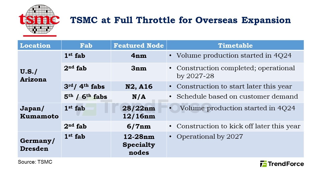
TSMC Expands U.S. Footprint with Two New Fabs in Arizona
TSMC is speeding up its plans to grow worldwide, the company's Chairman, C.C. Wei is announcing they'll start building their third and fourth fabs in Arizona later this year. This comes after TSMC finished constructing the second Arizona plant while the first fab started volume production in Q4 2024. TSMC wants to open its second factory about six months earlier than planned due to increasing customer demand. The first factory will make 4 nm chips, the second will target 3 nm chips, and the newer ones will work on even smaller N2 and A16 nodes. This rapid expansion is part of TSMC's additional $100 billion investment to build five more semiconductor plants and a research center in the U.S. In total, TSMC will invest $165 billion in the United States.
Besides its US operations, TSMC keeps pushing forward with its worldwide manufacturing plans. Wei dismissed rumors of setbacks at the company's upcoming Kumamoto plant in Japan. He confirmed that their first fab started mass production in late 2024, achieving excellent yields. They plan to begin building a second Japanese facility this year, once the infrastructure is ready. The company's European expansion in Dresden is also on track, with strong backing from both the European Commission and the German federal government. They broke ground at the Dresden site in August 2024 as Europe's first FinFET-capable dedicated foundry operation.

Besides its US operations, TSMC keeps pushing forward with its worldwide manufacturing plans. Wei dismissed rumors of setbacks at the company's upcoming Kumamoto plant in Japan. He confirmed that their first fab started mass production in late 2024, achieving excellent yields. They plan to begin building a second Japanese facility this year, once the infrastructure is ready. The company's European expansion in Dresden is also on track, with strong backing from both the European Commission and the German federal government. They broke ground at the Dresden site in August 2024 as Europe's first FinFET-capable dedicated foundry operation.

Sony Reportedly Prepping "PlayStation 6 Portable" with "<40 CU" Chipset Design
Sony and Microsoft seem to be involved in the development of handheld gaming consoles, but insiders reckon that respective next-generation offerings will not directly compete with each other. Xbox and ASUS have signalled some sort of collaborative ROG Alloy-esque device; potentially releasing later on in 2025. Whispers of a futuristic PlayStation portable model's chipset design emerged mid-way through March; courtesy of Kepler_L2. The notorious leaker has recent history of reporting inside track knowledge of AMD CPU and GPU architectures/technologies. They alleged that Sony and Team Red's collaborative PS6 APU design project had reached a finalized stage of development, possibly around late 2024/early 2025. Returning to March/April events; Kepler_L2 theorized that a "PS6 Portable" would not be capable of surpassing PlayStation 5 (home console) level performance upon launch in 2028.
The mysterious handheld is said to be powered by a "15 W SoC" manufactured on a non-specific 3 nm node process. Elaborating further, they posit that PlayStation's rumored handheld is capable of running PS5 generation games—bandwidth and power restrictions could reduce resolution and frame rates below that of Sony's current-gen system. Kepler_L2 pictures "PS6 Portable" gaming performance being somewhere in-between Xbox Series S and PlayStation 5 (non-Pro). According to rumors, the handheld's chipset is not related or derived from the PS6 home console's internal setup. Kepler_L2 envisioned a mobile SoC with fewer than 40 compute units (CUs)—several media outlets have added their interpretation of this data point; with a sub-36 count. PlayStation 5's GPU aspect consists of 36 CUs, while the Xbox Series S graphics solution makes do with 20 units. Sony's speculated return to portable territories will be welcomed by owners of older handheld models—namely the Vita and PSP. Famously, these portable products struggled to keep up with competing Nintendo devices.


The mysterious handheld is said to be powered by a "15 W SoC" manufactured on a non-specific 3 nm node process. Elaborating further, they posit that PlayStation's rumored handheld is capable of running PS5 generation games—bandwidth and power restrictions could reduce resolution and frame rates below that of Sony's current-gen system. Kepler_L2 pictures "PS6 Portable" gaming performance being somewhere in-between Xbox Series S and PlayStation 5 (non-Pro). According to rumors, the handheld's chipset is not related or derived from the PS6 home console's internal setup. Kepler_L2 envisioned a mobile SoC with fewer than 40 compute units (CUs)—several media outlets have added their interpretation of this data point; with a sub-36 count. PlayStation 5's GPU aspect consists of 36 CUs, while the Xbox Series S graphics solution makes do with 20 units. Sony's speculated return to portable territories will be welcomed by owners of older handheld models—namely the Vita and PSP. Famously, these portable products struggled to keep up with competing Nintendo devices.


Qualcomm's Upcoming Snapdragon X2 Elite PC to Get a 22% Performance Boost
Qualcomm aims to boost the performance of its Windows‑on‑Arm PC chips by about 18-22% percent with the next‑generation Snapdragon X2 processors. That estimate comes from Focused Digital, a well‑known Chinese blogger often leaks supply‑chain details. He says these new Snapdragon X2 chips will hit boost clocks of around 4.40 GHz, which is up from the 4.0 to 4.30 GHz range we see on today's Snapdragon X Elite models. Currently, those Elite chips use Oryon cores built on the TSMC 4 nm‑class N4P process. They run between 3.0 and 3.80 GHz at base and can turbo up to 4.30 GHz. So, simply cranking the top speed up another 100 MHz could explain a chunk of that performance jump. Beyond clocks, Qualcomm is probably squeezing more efficiency out of its Oryon V3 microarchitecture too, though we don't have details yet.
We also don't know exactly which process node Qualcomm will pick. They could stick with a refined 4 nm variant or switch to 3 nm later on. Either way, a roughly 20 percent improvement aligns with what you'd expect from a new generation of chips due in 2025. Another rumor floating around is that the X2 Elite series will jump from 12 to 18 cores, giving the processors more parallel horsepower. Internal test rigs reportedly pair these chips with up to 48 GB of LPDDR5X RAM and 1 TB of NVMe storage. Qualcomm rolled out its first Snapdragon X Elite processors in mid‑2024 and began testing the SC8480XP prototype in September 2024. If these performance figures hold up, the new Snapdragon X2 lineup could close the gap on x86 competitors and set Qualcomm up nicely for competing in stronger with a push in the PC segment by 2026.
We also don't know exactly which process node Qualcomm will pick. They could stick with a refined 4 nm variant or switch to 3 nm later on. Either way, a roughly 20 percent improvement aligns with what you'd expect from a new generation of chips due in 2025. Another rumor floating around is that the X2 Elite series will jump from 12 to 18 cores, giving the processors more parallel horsepower. Internal test rigs reportedly pair these chips with up to 48 GB of LPDDR5X RAM and 1 TB of NVMe storage. Qualcomm rolled out its first Snapdragon X Elite processors in mid‑2024 and began testing the SC8480XP prototype in September 2024. If these performance figures hold up, the new Snapdragon X2 lineup could close the gap on x86 competitors and set Qualcomm up nicely for competing in stronger with a push in the PC segment by 2026.

Xiaomi's Proprietary Flagship Mobile SoC Reportedly Downgraded to TSMC "N4P"
According to reports from last year, Xiaomi was expected to unveil an oft-rumored proprietary mobile chipset design at some point in 2025. By October 2024, the Chinese technology giant allegedly reached the tape-out phase of its first 3 nm SoC—at the time, insiders posited that Xiaomi was seeking a manufacturing partner. Months earlier, a prototype design was linked to TSMC's 4 nm "N4P" node process—this rumor raised many smartphone watchdog eyebrows. Unlike many other Chinese firms, Xiaomi was reportedly allowed to select a fairly advanced manufacturing process at Taiwan's premier foundry service. In a past weekend news article, Wccftech outlined interesting circumstances: "(US) export controls have yet to affect Xiaomi, which is supposedly on track to launch its first in-house chipset later this year. However, while we reported last year that the company was scheduled to unveil its custom 3 nm SoC in 2025, we were disappointed to learn just the specifications of this version that will utilize TSMC's 'N4P' process. According to more details, this silicon will not sport any homegrown cores like Qualcomm has adopted for the Snapdragon 8 Elite."
Late last week, Jukanlosreve highlighted another leaker's prediction—regarding the technological foundations of Xiaomi's mystery flagship mobile processor. Fixed Focus Digital's Weibo post mentioned the "N4P" node, as well the utilization of current generation Arm Cortex-X925, Cortex-A725 and Cortex-A520 units. A speculated Imagination Technologies "IMG DXT 72-2304" integrated graphics solution is touted to outperform Qualcomm's Adreno 740 iGPU; as featured in their Snapdragon 8 Gen 2 (2022) SoC. As highlighted by Wccftech's report, one of the publication's associates has deemed Fixed Focus Digital to be an unreliable source of inside track info. In response to Jukanlosreve's tweeted question, Mochamad Farido Fanani opined: "that's right, how does Xiaomi use N4P in its new chipset? But this guy always guesses blindly." Older leaks—based on "N4P" rumors—projected performance levels roughly on par with Qualcomm's first generation Snapdragon 8 chip. This model was introduced at the tail end of 2021.


Late last week, Jukanlosreve highlighted another leaker's prediction—regarding the technological foundations of Xiaomi's mystery flagship mobile processor. Fixed Focus Digital's Weibo post mentioned the "N4P" node, as well the utilization of current generation Arm Cortex-X925, Cortex-A725 and Cortex-A520 units. A speculated Imagination Technologies "IMG DXT 72-2304" integrated graphics solution is touted to outperform Qualcomm's Adreno 740 iGPU; as featured in their Snapdragon 8 Gen 2 (2022) SoC. As highlighted by Wccftech's report, one of the publication's associates has deemed Fixed Focus Digital to be an unreliable source of inside track info. In response to Jukanlosreve's tweeted question, Mochamad Farido Fanani opined: "that's right, how does Xiaomi use N4P in its new chipset? But this guy always guesses blindly." Older leaks—based on "N4P" rumors—projected performance levels roughly on par with Qualcomm's first generation Snapdragon 8 chip. This model was introduced at the tail end of 2021.


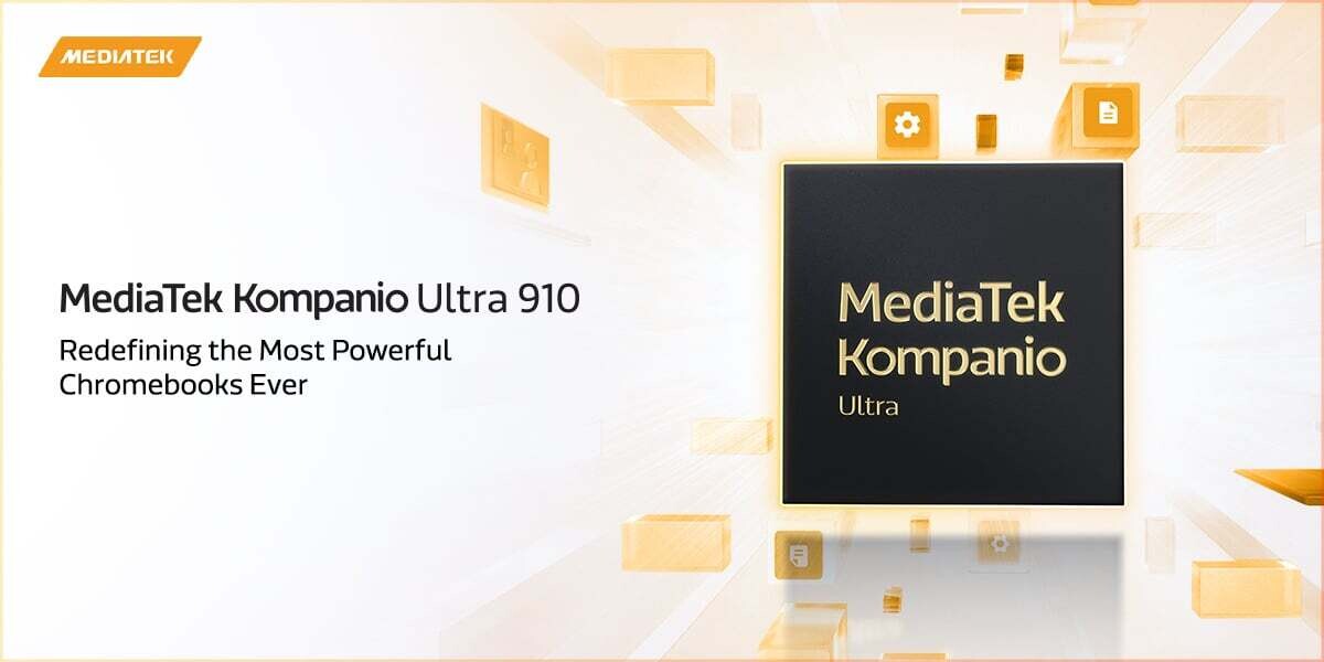
MediaTek Introduces Kompanio Ultra SoC, Touted to Redefine AI Performance for Chromebook Plus
MediaTek has introduced the Kompanio Ultra, the latest milestone in AI-powered, high-performance Chromebooks. Leveraging MediaTek's proven expertise in flagship innovation, this powerful new platform brings fantastic on-device AI capabilities, superior computing performance, and industry-leading power efficiency to the newest Chromebook Plus devices. "The Kompanio Ultra underscores our commitment to delivering groundbreaking computing performance and efficiency that MediaTek has shown as a leader in the mobile compute space for many years," said Adam King, Vice President & General Manager of Computing and Multimedia Business at MediaTek. "We worked closely with Google to ensure the newest Chromebook Plus devices enjoy next-generation on-device AI capabilities, superior performance per watt, and immersive multimedia."
The Kompanio Ultra is MediaTek's most powerful Chromebook processor to date, integrating 50 TOPS of AI processing power to enable on-device generative AI experiences. With MediaTek's 8th-generation NPU, users can expect real-time task automation, personalized computing, and seamless AI-enhanced workflows—with local processing for enhanced speed, security, efficiency, and support for AI workloads without an internet connection. Built on the cutting-edge (TSMC) 3 nm process, the Kompanio Ultra features an all-big-core CPU architecture with an Arm Cortex-X925 processor clocked at up to 3.62 GHz, delivering industry-leading single and multithreaded performance. Whether handling intensive applications like video editing, content creation, or high-resolution gaming, this processor ensures smooth, lag-free performance with unmatched multitasking capabilities.


The Kompanio Ultra is MediaTek's most powerful Chromebook processor to date, integrating 50 TOPS of AI processing power to enable on-device generative AI experiences. With MediaTek's 8th-generation NPU, users can expect real-time task automation, personalized computing, and seamless AI-enhanced workflows—with local processing for enhanced speed, security, efficiency, and support for AI workloads without an internet connection. Built on the cutting-edge (TSMC) 3 nm process, the Kompanio Ultra features an all-big-core CPU architecture with an Arm Cortex-X925 processor clocked at up to 3.62 GHz, delivering industry-leading single and multithreaded performance. Whether handling intensive applications like video editing, content creation, or high-resolution gaming, this processor ensures smooth, lag-free performance with unmatched multitasking capabilities.


Apple Reportedly Eyeing Late 2025 Launch of M5 MacBook Pro Series, M5 MacBook Air Tipped for 2026
Mark Gurman—Bloomberg's resident soothsayer of Apple inside track info—has disclosed predictive outlooks for next-generation M5 chip-based MacBooks. Early last month, we experienced the launch of the Northern Californian company's M4 MacBook Air series—starting at $999; also available in a refreshing metallic blue finish. The latest iteration of Apple's signature "extra slim" notebook family arrived with decent performance figures. As per usual, press and community attention has turned to a potential successor. Gurman's (March 30) Power On newsletter posited that engineers are already working on M5-powered super slim sequels—he believes that these offerings will arrive early next year, potentially reusing the current generation's 15-inch and 13-inch fanless chassis designs.
In a mid-February predictive report, Gurman theorized that Apple was planning a major overhaul of the MacBook Pro design. A radical reimagining of the long-running notebook series—that reportedly utilizes M6 chipsets and OLED panels—is a distant prospect; perhaps later on in 2026. The Cupertino-headquartered megacorp is expected to stick with its traditional release cadence, so 2025's "M5" refresh of MacBook Pro models could trickle out by October. Insiders believe that Apple will reuse existing MacBook Pro shells—the last major redesign occurred back in 2021. According to early February reportage, mass production of the much-rumored M5 chip started at some point earlier in the year. Industry moles posit that a 3 nm (N3P) node process was on the order books, chez TSMC foundries.


In a mid-February predictive report, Gurman theorized that Apple was planning a major overhaul of the MacBook Pro design. A radical reimagining of the long-running notebook series—that reportedly utilizes M6 chipsets and OLED panels—is a distant prospect; perhaps later on in 2026. The Cupertino-headquartered megacorp is expected to stick with its traditional release cadence, so 2025's "M5" refresh of MacBook Pro models could trickle out by October. Insiders believe that Apple will reuse existing MacBook Pro shells—the last major redesign occurred back in 2021. According to early February reportage, mass production of the much-rumored M5 chip started at some point earlier in the year. Industry moles posit that a 3 nm (N3P) node process was on the order books, chez TSMC foundries.


Qualcomm "Snapdragon 8 Elite Gen 2" Leak Points to Adreno 840 iGPU & Support of ARM's Latest Scalable Instruction Sets
Digital Chat Station (DCS)—a tenured leaker of Qualcomm pre-release information—has shared new "Snapdragon 8 Elite Gen 2" chipset details. Earlier today, their Weibo feed was updated with a couple of technological predictions. The announced smartphone chip's "SM8850" identifier was disclosed once again, along with the repeated claim that Qualcomm has selected a 3 nm "N3P" node process. Industry watchdogs expect to see the San Diego-headquartered fabless semiconductor designer introduce its next-generation flagship smartphone SoC in October. The current-gen Snapdragon 8 Elite platform was unveiled last Fall; sporting cutting-edge "Oryon" (aka Phoenix) processor cores and an integrated Adreno 830 graphics solution. DCS reckons that the natural successor will reuse a familiar "2 + 6" core configuration; comprised of two prime "big performance" units, and six "normal" performance-tuned units. An Adreno 840 iGPU was listed as DCS's final point of conjecture.
The incoming "Snapdragon 8 Elite Gen 2" chipset was mentioned in the same sentence as rumored "Pegasus" cores (Phoenix's sequel)—slightly far-fetched rumors from 2024 suggested Qualcomm's upgraded processor architecture being tested at maximum frequencies of 5.0 GHz (on performance cores). As pointed out by Wccftech, Gen 1's performance cores run at 4.47 GHz (by default). In today's follow-up post, DCS claimed that Qualcomm's: "self-developed CPU architecture is now in the second generation, with a performance setting of over 380 W+." Industry watchdogs reckon that the "Snapdragon 8 Elite 2" chip will be capable of recording 3.8+ million point tallies in AnTuTu V10 gauntlets, thanks to the alleged utilization of ArmV9 architecture. DCS theorized that the speculated "SM8850" SoC will support ARM's Scalable Matrix Extension 1 (SME 1) and Scalable Vector Extension 2 (SVE2) instruction sets.


The incoming "Snapdragon 8 Elite Gen 2" chipset was mentioned in the same sentence as rumored "Pegasus" cores (Phoenix's sequel)—slightly far-fetched rumors from 2024 suggested Qualcomm's upgraded processor architecture being tested at maximum frequencies of 5.0 GHz (on performance cores). As pointed out by Wccftech, Gen 1's performance cores run at 4.47 GHz (by default). In today's follow-up post, DCS claimed that Qualcomm's: "self-developed CPU architecture is now in the second generation, with a performance setting of over 380 W+." Industry watchdogs reckon that the "Snapdragon 8 Elite 2" chip will be capable of recording 3.8+ million point tallies in AnTuTu V10 gauntlets, thanks to the alleged utilization of ArmV9 architecture. DCS theorized that the speculated "SM8850" SoC will support ARM's Scalable Matrix Extension 1 (SME 1) and Scalable Vector Extension 2 (SVE2) instruction sets.


TSMC Accelerates US "Fab 21" Expansion Following Early Setbacks
TSMC is reconfiguring its US strategy after a challenging start at its Fab 21 facility near Phoenix, Arizona. The company's initial module took nearly five years to move from groundbreaking to production—far longer than the typical two-year process observed in Taiwan. Early setbacks, including labor issues, rising costs, and cultural differences, slowed progress, but these hurdles have provided valuable lessons. With a clearer understanding of the local construction environment, TSMC plans to speed up future projects. Company executives have identified reliable local contractors and addressed many bottlenecks that once hindered progress. As a result, the Taiwanese maker is gearing up to accelerate construction timelines for its upcoming modules. Notably, TSMC intends to start building its third fab—Fab 21 module 3—this year, aiming for a pace similar to that in Taiwan.
In the current phase, TSMC is finalizing equipment installations for Fab 21 module 1 while laying the groundwork for module 2. The plan is to begin trial production of advanced 3 nm-class chips at module 2 in 2026, with high-volume manufacturing expected to kick off by 2028. The accelerated schedule for module 3 is seen as a pathway to faster production of next-generation chips, including those using the N2-series and A16 process technologies. However, rapid construction is not without risks. A critical concern remains the timely procurement of essential fab tools. Leading suppliers such as ASML and Applied Materials face significant backlogs and capacity constraints, which may delay the delivery of necessary equipment. As TSMC vows to build its US capacity more swiftly, the entire supply chain is watching closely to see if these supply chain challenges can be resolved, ensuring that the company meets its ambitious production timelines while expanding its foothold in the American market.
In the current phase, TSMC is finalizing equipment installations for Fab 21 module 1 while laying the groundwork for module 2. The plan is to begin trial production of advanced 3 nm-class chips at module 2 in 2026, with high-volume manufacturing expected to kick off by 2028. The accelerated schedule for module 3 is seen as a pathway to faster production of next-generation chips, including those using the N2-series and A16 process technologies. However, rapid construction is not without risks. A critical concern remains the timely procurement of essential fab tools. Leading suppliers such as ASML and Applied Materials face significant backlogs and capacity constraints, which may delay the delivery of necessary equipment. As TSMC vows to build its US capacity more swiftly, the entire supply chain is watching closely to see if these supply chain challenges can be resolved, ensuring that the company meets its ambitious production timelines while expanding its foothold in the American market.


AMD Ryzen AI "Medusa Point" APU Could Arrive with Larger Footprint - BGA "FP10" Dimensions Leaked
Shipping manifests have served as fairly reliable sources of pre-launch information—Everest (aka Olrak29) has discovered many juicy details in recent times. Their latest sleuthing session—combing through NBD documents—has indicated AMD's (alleged) prepping of a larger socket design for next-generation mobile processors. A leaked document alludes to the existence of various "MEDUSA01" jig and block "FP10" socket validation parts. Current-generation Ryzen AI "Strix Point" 300 series APUs utilize the FP8 socket format. Based on the "MEDUSA01" shipping manifest, it seems that a successor will arrive with a larger footprint—measurements of 25 mm x 42.5 mm are repeated throughout the leaked description list. Industry watchdogs surmise that "Medusa Point's" BGA FP10 socket will be approximately 6% larger than its predecessor.
Mid-way through last month, insider theorizations pointed to "Medusa Point" being a chiplet-based design. A "single 12-core Zen 6 CCD" was linked to a TSMC 3 nm-class node, with "N4P" reportedly selected for a separate mobile client I/O die. Readily available 4 nm Ryzen AI "Strix Point" processors are monolithic in nature. Initial inside track info mentioned RDNA 4 technology in the same equation as "Medusa Point," but recent Team Red's recent-ish targeting of "GFX1153" places RDNA 3.5 as the de facto choice.

Mid-way through last month, insider theorizations pointed to "Medusa Point" being a chiplet-based design. A "single 12-core Zen 6 CCD" was linked to a TSMC 3 nm-class node, with "N4P" reportedly selected for a separate mobile client I/O die. Readily available 4 nm Ryzen AI "Strix Point" processors are monolithic in nature. Initial inside track info mentioned RDNA 4 technology in the same equation as "Medusa Point," but recent Team Red's recent-ish targeting of "GFX1153" places RDNA 3.5 as the de facto choice.


Industry Analyst Walks Back Claim about Apple A20 SoC Using N3P, Repredicts TSMC 2 nm
Earlier in the week, Apple specialist press outlets picked up on a noted industry analyst's technological forecast for a future iPhone processor design. Jeff Pu—of GF Industries, Hong Kong—predicted that the next-generation A20 SoC would be produced via a TSMC 3 nm (N3P) nodes process. Despite rumors of Apple gaining front row seats at the "2 nm ballgame," the partnership between fabless chip designer and foundry could potentially revisit already covered ground. The A19 chipset was previously linked to N3P (by insiders), with Pu expressing the belief that A20 would utilize the same fundamental lithographic underpinnings; albeit enhanced with TSMC's Chip on Wafer on Substrate (CoWoS) packaging technology (for AI improvements).
This morning, MacRumors followed up on their initial news article—they reported that "wires were crossed" at GF Industries, regarding projections for the (2026) iPhone 18 generation. The publication received direct feedback from the man of the hour: "Jeff Pu (lead Apple analyst) has since clarified that he believes the A20 chip will be manufactured with the N2 process, so the information about the chip using the N3P process should be disregarded. Earlier reports had said the A20 chip would be 2 nm, so rumors align again. This is ultimately good news, as it means the A20 chip should have more substantial performance and power efficiency improvements over the A19 chip." Cutting-edge smartphone processor enthusiasts expressed much disappointment when A20 was (regressively) linked to N3P; the latest revisement should instill some joy. According to industry moles, TSMC is making good progress with its cutting-edge 2 nm node process—mass production is expected to start at some point within the second half of 2025.


This morning, MacRumors followed up on their initial news article—they reported that "wires were crossed" at GF Industries, regarding projections for the (2026) iPhone 18 generation. The publication received direct feedback from the man of the hour: "Jeff Pu (lead Apple analyst) has since clarified that he believes the A20 chip will be manufactured with the N2 process, so the information about the chip using the N3P process should be disregarded. Earlier reports had said the A20 chip would be 2 nm, so rumors align again. This is ultimately good news, as it means the A20 chip should have more substantial performance and power efficiency improvements over the A19 chip." Cutting-edge smartphone processor enthusiasts expressed much disappointment when A20 was (regressively) linked to N3P; the latest revisement should instill some joy. According to industry moles, TSMC is making good progress with its cutting-edge 2 nm node process—mass production is expected to start at some point within the second half of 2025.


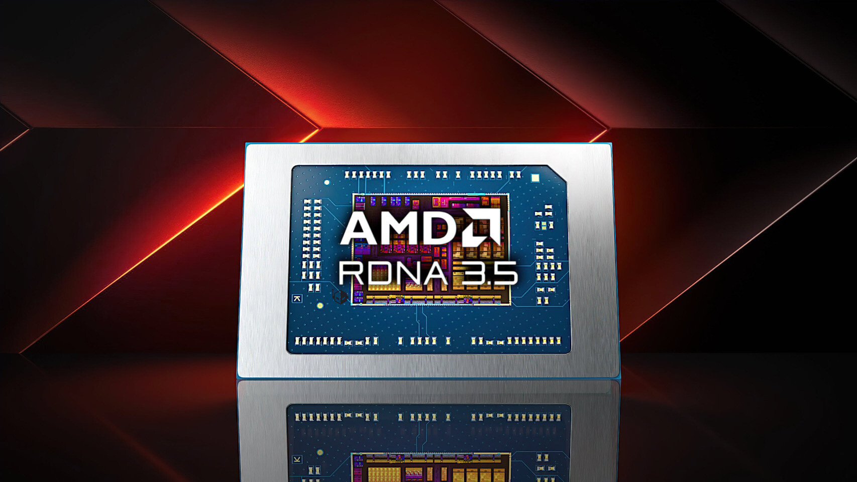
AMD "Medusa Point" APU with Zen 6 Confirmed to Use RDNA 3.5, RDNA 4 Reserved for Discrete GPUs
AMD's next-generation Zen 6-based "Medusa Point" mobile APUs will not feature RDNA 4 graphics as previously speculated, according to recent code discoveries in AMD GPUOpen Drivers on GitHub. The Device ID "GfxIp12" associated with RDNA 4 architecture has been reserved only for discrete GPUs, confirming that the current Radeon RX 9000 series will exclusively implement AMD's latest graphics architecture. Current technical documentation indicates AMD will instead extend RDNA 3.5 implementation beyond the Zen 5 portfolio while potentially positioning UDNA as the successor technology for integrated graphics.
The chiplet-based Medusa Point design will reportedly pair a single 12-core Zen 6 CCD manufactured on TSMC's 3 nm-class node with a mobile client I/O die likely built on N4P. This arrangement is significantly different from current monolithic mobile solutions. Earlier speculation indicates the Medusa Point platform may support 3D V-Cache variants, leveraging the same vertical stacking methodology employed in current Zen 5 implementations. The mobile processor's memory controllers and neural processing unit are expected to receive substantial updates. However, compatibility limitations with AMD's latest graphics features, like FSR 4 technology, remain a concern due to the absence of RDNA 4 silicon. The Zen 6-powered Medusa Point processor family is scheduled for release in 2026, targeting premium mobile computing applications with a performance profile that builds upon AMD's current Strix Halo positioning.
The chiplet-based Medusa Point design will reportedly pair a single 12-core Zen 6 CCD manufactured on TSMC's 3 nm-class node with a mobile client I/O die likely built on N4P. This arrangement is significantly different from current monolithic mobile solutions. Earlier speculation indicates the Medusa Point platform may support 3D V-Cache variants, leveraging the same vertical stacking methodology employed in current Zen 5 implementations. The mobile processor's memory controllers and neural processing unit are expected to receive substantial updates. However, compatibility limitations with AMD's latest graphics features, like FSR 4 technology, remain a concern due to the absence of RDNA 4 silicon. The Zen 6-powered Medusa Point processor family is scheduled for release in 2026, targeting premium mobile computing applications with a performance profile that builds upon AMD's current Strix Halo positioning.
Apple "A20" SoC Linked to TSMC "N3P" Process, AI Aspect Reportedly Improved with Advanced Packaging Tech
Over a year ago, industry watchdogs posited that Apple was patiently waiting in line at the front of TSMC's 2 Nanometer GAA "VVIP queue." The securing of cutting-edge manufacturing processes seems to be a consistent priority for the Cupertino, California-headquartered fabless chip designer. Current generation Apple chipsets—at best—utilize TSMC 3 nm (N3E) wafers. Up until very recently, many insiders believed that the projected late 2026 launch of A20 SoC-powered iPhone 18 smartphones would signal a transition to the Taiwanese foundry's advanced 2 nm (N2) node process. Officially, TSMC has roadmapped the start of 2 nm mass production around the second half of 2025.
According to Jeff Pu—a Hong Kong-based analyst at GF Securities—the speculated A20 (2026) chipset could stick with N3P. Leaks suggest that aspects of Apple's next in line "A19" and "A19 Pro" mobile SoCs could be produced via a 3 nm TSMC process. MacRumors has picked up on additional inside track whispers; about Apple M5 processors (for next-gen iPad Pro models) being based on N3P—"likely due to increased wafer costs." Pu reckons that Apple's engineering team has provisioned a major generational improvement with A20's AI capabilities, courtesy of TSMC's Chip on Wafer on Substrate (CoWoS) packaging technology. This significant upgrade is touted to tighten integration between the chip's processor, unified memory, and Neural Engine segments. Revised insider forecasts have positioned A21 chip designs as natural candidates for a shift into 2 nm GAA territories.


According to Jeff Pu—a Hong Kong-based analyst at GF Securities—the speculated A20 (2026) chipset could stick with N3P. Leaks suggest that aspects of Apple's next in line "A19" and "A19 Pro" mobile SoCs could be produced via a 3 nm TSMC process. MacRumors has picked up on additional inside track whispers; about Apple M5 processors (for next-gen iPad Pro models) being based on N3P—"likely due to increased wafer costs." Pu reckons that Apple's engineering team has provisioned a major generational improvement with A20's AI capabilities, courtesy of TSMC's Chip on Wafer on Substrate (CoWoS) packaging technology. This significant upgrade is touted to tighten integration between the chip's processor, unified memory, and Neural Engine segments. Revised insider forecasts have positioned A21 chip designs as natural candidates for a shift into 2 nm GAA territories.


GUC Launches First 32 Gbps per Lane UCIe Silicon Using TSMC 3nm and CoWoS Technology
Global Unichip Corp. (GUC), the Advanced ASIC Leader, today announced the successful launch of industry's first Universal Chiplet Interconnect Express (UCIe) PHY silicon, achieving a data rate of 32 Gbps per lane, the highest speed defined in the UCIe specification. The 32G UCIe IP, supporting UCIe 2.0, delivers an impressive bandwidth density of 10 Tbps per 1 mm of die edge (5 Tbps/mm full-duplex). This milestone was achieved using TSMC's advanced N3P process and CoWoS packaging technologies, targeting AI, high-performance computing (HPC), xPU, and networking applications.
In this test chip, several dies with North-South and East-West IP orientations are interconnected through CoWoS interposer. The silicon measurements show robust 32 Gbps operation with wide horizontal and vertical eye openings. GUC is working aggressively on the full-corner qualification, and the complete silicon report is expected to be available in the coming quarter.
In this test chip, several dies with North-South and East-West IP orientations are interconnected through CoWoS interposer. The silicon measurements show robust 32 Gbps operation with wide horizontal and vertical eye openings. GUC is working aggressively on the full-corner qualification, and the complete silicon report is expected to be available in the coming quarter.

Chinese Researchers Develop No-Silicon 2D GAAFET Transistor Technology
Scientists from Beijing University have developed the world's first two-dimensional gate-all-around field-effect transistor (GAAFET), establishing a new performance benchmark in domestic semiconductor design. The design, documented in Nature, represents a difference in transistor architecture that could reshape the future of Chinese microelectronics design. Given the reported characteristic of 40% higher performance and 10% improved efficiency compared to the TSMC 3 nm N3 node, it looks rather promising. The research team, headed by Professors Peng Hailin and Qiu Chenguang, engineered a "wafer-scale multi-layer-stacked single-crystalline 2D GAA configuration" that demonstrated superior performance metrics when benchmarked against current industry leaders. The innovation leverages bismuth oxyselenide (Bi₂O₂Se), a novel semiconductor material that maintains exceptional carrier mobility at sub-nanometer dimensions—a critical advantage as the industry struggles to push angstrom-era semiconductor nodes.
"Traditional silicon-based transistors face fundamental physical limitations at extreme scales," explained Professor Peng, who characterized the technology as "the fastest, most efficient transistor ever developed." The 2D GAAFET architecture circumvents the mobility degradation that plagues silicon in ultra-small geometries, allowing for continued performance scaling beyond current nodes. The development comes during China's intensified efforts to achieve semiconductor self-sufficiency, as trade restrictions have limited access to advanced lithography equipment and other critical manufacturing technologies. Even with China developing domestic EUV technology, it is still not "battle" proven. Rather than competing directly with established fabrication processes, the Beijing team has pioneered an entirely different technological approach—what Professor Peng described as "changing lanes entirely" rather than seeking incremental improvements, where China can not compete in the near term.
"Traditional silicon-based transistors face fundamental physical limitations at extreme scales," explained Professor Peng, who characterized the technology as "the fastest, most efficient transistor ever developed." The 2D GAAFET architecture circumvents the mobility degradation that plagues silicon in ultra-small geometries, allowing for continued performance scaling beyond current nodes. The development comes during China's intensified efforts to achieve semiconductor self-sufficiency, as trade restrictions have limited access to advanced lithography equipment and other critical manufacturing technologies. Even with China developing domestic EUV technology, it is still not "battle" proven. Rather than competing directly with established fabrication processes, the Beijing team has pioneered an entirely different technological approach—what Professor Peng described as "changing lanes entirely" rather than seeking incremental improvements, where China can not compete in the near term.


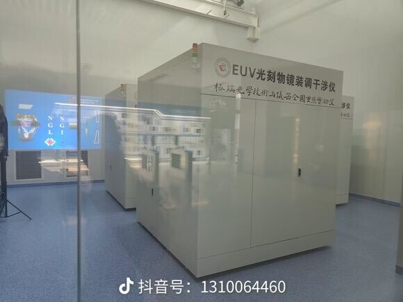
China Develops Domestic EUV Tool, ASML Monopoly in Trouble
China's domestic extreme ultraviolet (EUV) lithography development is far from a distant dream. The newest system, now undergoing testing at Huawei's Dongguan facility, leverages laser-induced discharge plasma (LDP) technology, representing a potentially disruptive approach to EUV light generation. The system is scheduled for trial production in Q3 2025, with mass manufacturing targeted for 2026, potentially positioning China to break ASML's technical monopoly in advanced lithography. The LDP approach employed in the Chinese system generates 13.5 nm EUV radiation by vaporizing tin between electrodes and converting it to plasma via high-voltage discharge, where electron-ion collisions produce the required wavelength. This methodology offers several technical advantages over ASML's laser-produced plasma (LPP) technique, including simplified architecture, reduced footprint, improved energy efficiency, and potentially lower production costs.
The LPP method relies on high-energy lasers and complex FPGA-based real-time control electronics to achieve the same result. While ASML has refined its LPP-based systems over decades, the inherent efficiency advantages of the LDP approach could accelerate China's catch-up timeline in this critical semiconductor manufacturing technology. When the US imposed sanctions on EUV shipments to Chinese companies, the Chinese semiconductor development was basically limited as standard deep ultraviolet (DUV) wave lithography systems utilize 248 nm (KrF) and 193 nm (ArF) wavelengths for semiconductor patterning, with 193 nm immersion technology representing the most advanced pre-EUV production technique. These longer wavelengths contrast with EUV's 13.5 nm radiation, requiring multiple patterning techniques to achieve advanced nodes.

The LPP method relies on high-energy lasers and complex FPGA-based real-time control electronics to achieve the same result. While ASML has refined its LPP-based systems over decades, the inherent efficiency advantages of the LDP approach could accelerate China's catch-up timeline in this critical semiconductor manufacturing technology. When the US imposed sanctions on EUV shipments to Chinese companies, the Chinese semiconductor development was basically limited as standard deep ultraviolet (DUV) wave lithography systems utilize 248 nm (KrF) and 193 nm (ArF) wavelengths for semiconductor patterning, with 193 nm immersion technology representing the most advanced pre-EUV production technique. These longer wavelengths contrast with EUV's 13.5 nm radiation, requiring multiple patterning techniques to achieve advanced nodes.

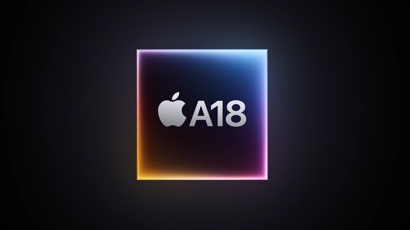
TSMC Set to Benefit from Estimated 22 Million Apple iPhone 16e Unit Sales
On Wednesday (February 19), Apple announced the upcoming launch of its "budget-friendly" iPhone 16e smartphone model. The Cupertino, California-based company has refreshed its entry level product tier—starting at $599—with modernized internals. Apple's new design houses an A18 chipset, as well as their much-discussed debut modem design. The C1 is a custom 5G part; fully developed in-house. Previously, modern iPhone product ranges have been fitted with Qualcomm 5G modems. As expected, Apple contracted with TSMC for the production of A18 and C1 silicon—the A-type SoC is based on a 3 nm process node (TSMC N3E). Their proprietary modem baseband design utilizes 4 mm, while the receiver uses a 7 nm process—according to insiders.
Taiwan's Commercial Times reckons that TSMC will be the "biggest beneficiary" from the aforementioned agreement with Apple. Ctee TW's latest report cites industry analysis; soothsayers estimate annual shipments reaching roughly 22 million units annually. Additional whispers suggest that the C1 modem will turn up in non-iPhone devices—namely next-gen Watches and iPads, by next year. The report also mentions that upcoming Mac products are slated for C1 upgrades. Further leaks have linked project "Ganymede" to a "C2" custom 5G modem design—inside sources believe that a 3 nm TSMC process is on the cards. Another codename—"Prometheus"—was leaked by insiders; possibly referencing a future "C3" model.


Taiwan's Commercial Times reckons that TSMC will be the "biggest beneficiary" from the aforementioned agreement with Apple. Ctee TW's latest report cites industry analysis; soothsayers estimate annual shipments reaching roughly 22 million units annually. Additional whispers suggest that the C1 modem will turn up in non-iPhone devices—namely next-gen Watches and iPads, by next year. The report also mentions that upcoming Mac products are slated for C1 upgrades. Further leaks have linked project "Ganymede" to a "C2" custom 5G modem design—inside sources believe that a 3 nm TSMC process is on the cards. Another codename—"Prometheus"—was leaked by insiders; possibly referencing a future "C3" model.


Samsung Boss Reportedly Encouraged Simultaneous Development of Exynos 2500 SoC & Galaxy S26 Series
The late 2024 news cycle suggested that Samsung's semiconductor business was going through tough times. Alleged yield problems—affecting the 3 nm Gate-All-Around (GAA) process—were highlighted last November. Fast-forward to January 2025; the South Korean megacorp has launched its cutting-edge Galaxy S25 smartphone series. The entire lineup of newly unveiled flagship smartphones contains Qualcomm's Snapdragon 8 Elite mobile chipsets; the Southern Californian chip designer is reportedly pulling in a tidy sum from this partnership. Fresh reports from South Korean news outlets indicate that Samsung System LSI employees have received an "encouraging" email from their boss, regarding current production predicaments.
Businesskorea and Sedaily reports include quotes extracted from the (apparently) leaked internal memo. LSI division president, Park Yong-in, reportedly stated: "we are currently in a situation where we have to develop two flagship products at the same time." Both articles allege that Samsung's semiconductor teams are expected to "cultivate roots and withstand storms." Industry watchdogs believe that the aforementioned "flagship products" are the Exynos 2500 mobile chipset, and Samsung Electronic's next-gen Galaxy S26 smartphone family. Earlier this month, we heard whispers about the much-delayed in-house chip design being readied (with a 2 nm process) for a possible late 2025 launch, inside unannounced Galaxy Z Flip 7 and Fold 7 devices. Park disclosed anticipated incoming obstacles in 2025: "last year's business division profit was higher than expected, but this was a temporary phenomenon...Looking at the entire business division, there will be monthly surpluses and deficits." Last month, inside sources proposed the notion that foundry investments were slashed in half.


Businesskorea and Sedaily reports include quotes extracted from the (apparently) leaked internal memo. LSI division president, Park Yong-in, reportedly stated: "we are currently in a situation where we have to develop two flagship products at the same time." Both articles allege that Samsung's semiconductor teams are expected to "cultivate roots and withstand storms." Industry watchdogs believe that the aforementioned "flagship products" are the Exynos 2500 mobile chipset, and Samsung Electronic's next-gen Galaxy S26 smartphone family. Earlier this month, we heard whispers about the much-delayed in-house chip design being readied (with a 2 nm process) for a possible late 2025 launch, inside unannounced Galaxy Z Flip 7 and Fold 7 devices. Park disclosed anticipated incoming obstacles in 2025: "last year's business division profit was higher than expected, but this was a temporary phenomenon...Looking at the entire business division, there will be monthly surpluses and deficits." Last month, inside sources proposed the notion that foundry investments were slashed in half.


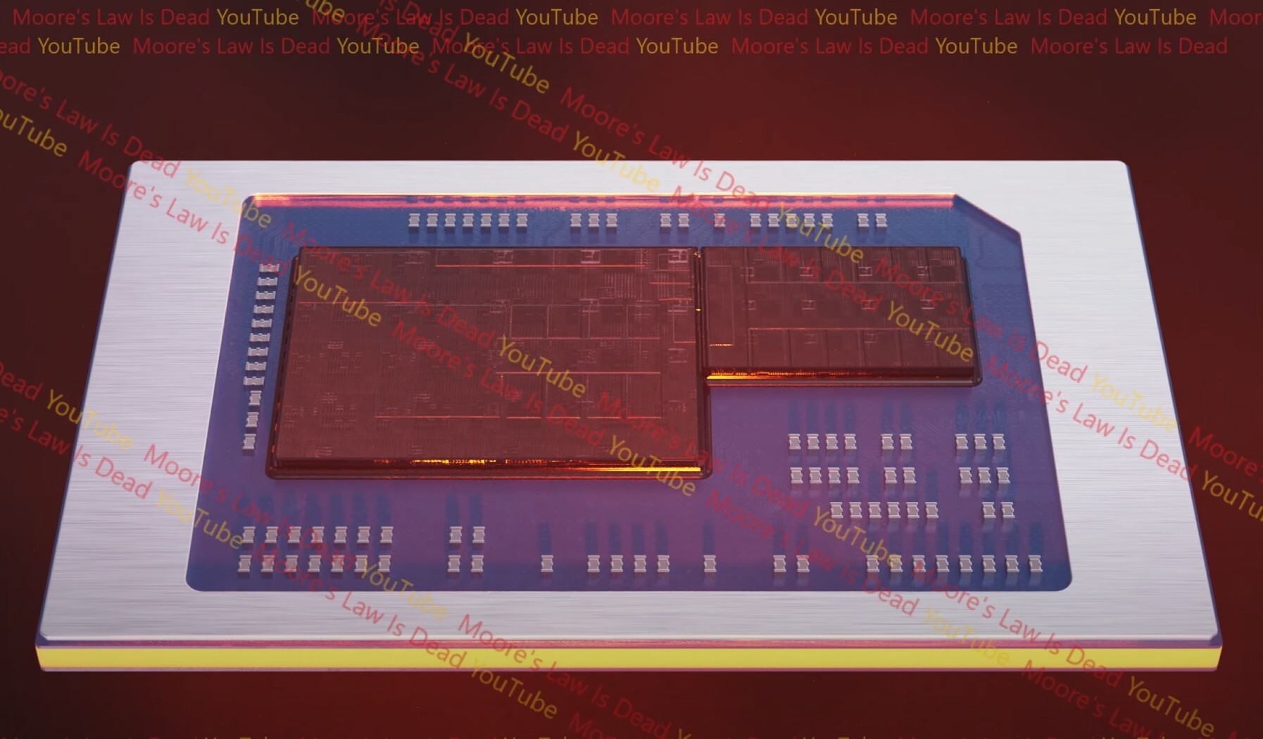
AMD Zen 6 Powers "Medusa Point" Mobile and "Olympic Ridge" Desktop Processors
AMD is readying two important client segment processors powered by the next-generation "Zen 6" microarchitecture, according to a sensational new report by Moore's Law is Dead. These are the "Medusa Point" mobile processor, and the "Olympic Ridge" desktop. The former is a BGA roughly the size and Z-Height of the current "Strix Point," but the latter is being designed for the existing Socket AM5, making it the third (and probably final) microarchitecture to do so. If you recall, Socket AM4 served three generations of Zen, not counting the refreshed "Zen+." At the heart of the effort is a new CPU complex die (CCD) that AMD plans to use across its client and server lineup.
The "Zen 6" performance CCD is being designed for a 3 nm-class node, likely the TSMC N3E. This node promises a significant increase in transistor density, power, and clock speed improvements over the current TSMC N4P node being used to build the "Zen 5" CCD. Here's where it gets interesting. The CCD contains twelve full-sized "Zen 6" cores, marking the first increase in core-counts of AMD's performance cores since its very first "Zen" CCD. All 12 of these cores are part of a single CPU core complex (CCX), and share a common L3 cache. There could be a proportionate increase in cache size to 48 MB. AMD is also expected to improve the way the CCDs communicate with the I/O die and among each other.


The "Zen 6" performance CCD is being designed for a 3 nm-class node, likely the TSMC N3E. This node promises a significant increase in transistor density, power, and clock speed improvements over the current TSMC N4P node being used to build the "Zen 5" CCD. Here's where it gets interesting. The CCD contains twelve full-sized "Zen 6" cores, marking the first increase in core-counts of AMD's performance cores since its very first "Zen" CCD. All 12 of these cores are part of a single CPU core complex (CCX), and share a common L3 cache. There could be a proportionate increase in cache size to 48 MB. AMD is also expected to improve the way the CCDs communicate with the I/O die and among each other.


TSMC Approves $17 Billion Investment to Expand Capacity, No Update on U.S. Strategy
TSMC has unveiled today its board meeting decisions, the chip giant has greenlit a massive US$17 billion investment to boost production capacity. According to TSMC, to meet long-term capacity plans based on market demand forecasts and TSMC's technology development roadmap, the board approved capital appropriations of approximately US$17.14 billion for installation and upgrade of advanced technology capacity, installation and upgrade of advanced packaging, mature and/or specialty technology capacity, fab construction, and installation of fab facility systems.
Previous reports by MoneyDJ suggested that TSMC might unveil plans for a third Arizona fab, a potential fourth fab, or its first advanced packaging plant after the board meeting. However, no updates have been confirmed yet. Industry sources suggested that TSMC's second Arizona fab, featuring 3 nm, will likely go ahead of schedule, providing a temporary response to U.S. pressures. According to the same report, TSMC's second Arizona fab is expected to begin equipment installation in mid-2026, with mass production expected by 2027. Notably, this progress would exceed TSMC's projections which expected the second plant to start 3 nm and 2 nm production in 2028, with a third plant potentially for the 2 nm process by the late 2030s. The MoneyDJ report further notes that initially, TSMC's second Arizona plant will offer 25K-30K 3 nm wafers per month. TSMC's first Arizona plant, initially slated for 2025, started 4 nm production ahead of schedule in Q4 2024.
Previous reports by MoneyDJ suggested that TSMC might unveil plans for a third Arizona fab, a potential fourth fab, or its first advanced packaging plant after the board meeting. However, no updates have been confirmed yet. Industry sources suggested that TSMC's second Arizona fab, featuring 3 nm, will likely go ahead of schedule, providing a temporary response to U.S. pressures. According to the same report, TSMC's second Arizona fab is expected to begin equipment installation in mid-2026, with mass production expected by 2027. Notably, this progress would exceed TSMC's projections which expected the second plant to start 3 nm and 2 nm production in 2028, with a third plant potentially for the 2 nm process by the late 2030s. The MoneyDJ report further notes that initially, TSMC's second Arizona plant will offer 25K-30K 3 nm wafers per month. TSMC's first Arizona plant, initially slated for 2025, started 4 nm production ahead of schedule in Q4 2024.

AMD to Build Zen 6 CCD on TSMC 3nm Process, Next-Gen cIOD and sIOD on 4nm
AMD is rumored to be building its next-generation CCD (core complex die) that implements the "Zen 6" microarchitecture, on the 3 nm TSMC N3E foundry node. This is part of a set of rumors from ChipHell forum, which got past rumors on AMD right. Apparently, AMD will also refresh the I/O dies for its next generation process, building them on the 4 nm foundry node, likely the TSMC N4C. The TSMC N3E node offers a 20% speed improvement, over 30% power savings, and approximately 60% logic density increase over TSMC N5, whereas the TSMC N4P node that the company uses for its current "Zen 5" chiplets only clock minor increases in logic density and power over N5. The N3E node relies on EUV double-patterning to achieve its logic density increases.
Perhaps the most interesting piece of news is the new-generation I/O dies. AMD is building these on the 4 nm node, which is a significant step up from the 6 nm node its current I/O dies are built on. On the client side of things, 4 nm will enable AMD to give the new cIOD an updated iGPU, probably based on a newer graphics architecture, such as RDNA 3.5. It will also give AMD the opportunity to integrate an NPU. The company might also update its key I/O components, such as the DDR5 memory controllers, to support higher memory speeds unlocked by CUDIMMs. We don't predict any updates on the PCIe front, since AMD is expected to carry on with Socket AM5, which determines that the cIOD puts out 28 PCIe Gen 5 lanes. At best, the USB interface put out from the processor could be updated to USB4 through an on-die host controller. Over on the server side, the new-generation sIOD will bring much needed increases to the DDR5 memory speeds enabled by clock drivers.
Perhaps the most interesting piece of news is the new-generation I/O dies. AMD is building these on the 4 nm node, which is a significant step up from the 6 nm node its current I/O dies are built on. On the client side of things, 4 nm will enable AMD to give the new cIOD an updated iGPU, probably based on a newer graphics architecture, such as RDNA 3.5. It will also give AMD the opportunity to integrate an NPU. The company might also update its key I/O components, such as the DDR5 memory controllers, to support higher memory speeds unlocked by CUDIMMs. We don't predict any updates on the PCIe front, since AMD is expected to carry on with Socket AM5, which determines that the cIOD puts out 28 PCIe Gen 5 lanes. At best, the USB interface put out from the processor could be updated to USB4 through an on-die host controller. Over on the server side, the new-generation sIOD will bring much needed increases to the DDR5 memory speeds enabled by clock drivers.
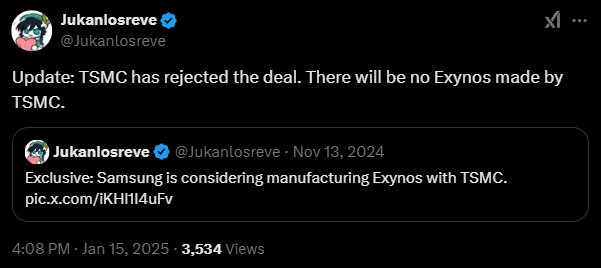
TSMC Reportedly Rejects Samsung's Proposed Exynos Mass Production Request
Samsung's native foundry operations have wrestled with the 3 nm Gate-All-Around (GAA) process—these problems have persisted since the first reports of "missed production targets" emerged late last year—online speculators floated a very disappointing yield figure: only 20%. Last December, industry moles proposed that the South Korean technology giant had devised plans to form an Exynos-centric "multi-channel partnership" with rival chipmakers. Speculation pointed to TSMC being the only valid ally. Semiconductor industry tipster—Jukanlosreve—believes that negotiations have taken place, and the answer was a firm "no." TSMC's most advanced node process order books are likely filled up with more important customers—industry watchdogs reckon that Apple usually gets first dibs.
Taiwan's top semiconductor manufacturer leads the market with its cutting-edge lithography techniques. Insiders believe that Samsung was impressed by TSMC's 2 nm trial production runs achieving (rumored) 60% yields. The higher-end Exynos chipsets are normally produced with the best node process available, but missed manufacturing goals have caused Samsung to drop in-house tech. In the recent past, Qualcomm's most powerful Snapdragon mobile chipsets have been deployed on flagship Galaxy S smartphones. Jukanlosreve believes that TSMC rejected Samsung's proposed Exynos deal due to a fear of revealing too many "trade secrets." Potentially, the South Koreans could have learned a thing or two about improving yields—courtesy of TSMC's expert knowledge.


Taiwan's top semiconductor manufacturer leads the market with its cutting-edge lithography techniques. Insiders believe that Samsung was impressed by TSMC's 2 nm trial production runs achieving (rumored) 60% yields. The higher-end Exynos chipsets are normally produced with the best node process available, but missed manufacturing goals have caused Samsung to drop in-house tech. In the recent past, Qualcomm's most powerful Snapdragon mobile chipsets have been deployed on flagship Galaxy S smartphones. Jukanlosreve believes that TSMC rejected Samsung's proposed Exynos deal due to a fear of revealing too many "trade secrets." Potentially, the South Koreans could have learned a thing or two about improving yields—courtesy of TSMC's expert knowledge.


TSMC Reports Record Q4 2024 Earnings with 37% YoY Growth
TSMC (TWSE: 2330, NYSE: TSM) today announced consolidated revenue of NT$868.46 billion, net income of NT$374.68 billion, and diluted earnings per share of NT$14.45 (US$2.24 per ADR unit) for the fourth quarter ended December 31, 2024. Year-over-year, fourth quarter revenue increased 38.8% while net income and diluted EPS both increased 57.0%. Compared to third quarter 2024, fourth quarter results represented a 14.3% increase in revenue and a 15.2% increase in net income. All figures were prepared in accordance with TIFRS on a consolidated basis.
In US dollars, fourth quarter revenue was $26.88 billion, which increased 37.0% year-over-year and increased 14.4% from the previous quarter. Gross margin for the quarter was 59.0%, operating margin was 49.0%, and net profit margin was 43.1%. In the fourth quarter, shipments of 3-nanometer accounted for 26% of total wafer revenue; 5-nanometer accounted for 34%; 7-nanometer accounted for 14%. Advanced technologies, defined as 7-nanometer and more advanced technologies, accounted for 74% of total wafer revenue.

In US dollars, fourth quarter revenue was $26.88 billion, which increased 37.0% year-over-year and increased 14.4% from the previous quarter. Gross margin for the quarter was 59.0%, operating margin was 49.0%, and net profit margin was 43.1%. In the fourth quarter, shipments of 3-nanometer accounted for 26% of total wafer revenue; 5-nanometer accounted for 34%; 7-nanometer accounted for 14%. Advanced technologies, defined as 7-nanometer and more advanced technologies, accounted for 74% of total wafer revenue.


Alphawave Semi Scales UCIe to 64 Gbps for 3nm Die-to-Die Chiplet Connectivity
Alphawave Semi (LSE: AWE), a global leader in high-speed connectivity and compute silicon for the world's technology infrastructure, proudly introduces the industry's first 64 Gbps Universal Chiplet Interconnect Express (UCIe) Die-to-Die (D2D) IP Subsystem to deliver unprecedented chiplet interconnect data rates, setting a new standard for ultra-high-performance D2D connectivity solutions in the industry. The third generation, 64 Gbps IP Subsystem builds on the successes of the most recent Gen 2 36 Gbps IP subsystem and silicon-proven Gen 1 24 Gbps and is available in TSMC's 3 nm Technology for both Standard and Advanced packaging. The silicon proven success and tapeout milestones pave the way for Alphawave Semi's Gen 3 UCIe IP subsystem offering.
Alphawave Semi is set to revolutionize connectivity with its Gen 3 64 Gbps UCIe IP, delivering a bandwidth density of over 20 Tbps/mm, with ultra-low power and latency. This solution is highly configurable supporting multiple protocols, including AXI-4, AXI-S, CXS, CHI and CHI-C2C to address the growing demands for high-performance connectivity across disaggregated systems in High-Performance Computing (HPC), Data Centers, and Artificial Intelligence (AI) applications.
Alphawave Semi is set to revolutionize connectivity with its Gen 3 64 Gbps UCIe IP, delivering a bandwidth density of over 20 Tbps/mm, with ultra-low power and latency. This solution is highly configurable supporting multiple protocols, including AXI-4, AXI-S, CXS, CHI and CHI-C2C to address the growing demands for high-performance connectivity across disaggregated systems in High-Performance Computing (HPC), Data Centers, and Artificial Intelligence (AI) applications.

Rapidus Installs Japan's First ASML NXE:3800E EUV Lithography Machine
Rapidus Corporation, a manufacturer of advanced logic semiconductors, today announced the delivery and installation of ASML's EUV lithography equipment at its Innovative Integration for Manufacturing (IIM-1) foundry, an advanced semiconductor development and manufacturing fab currently under construction in Chitose, Hokkaido. To commemorate the installation, a ceremony was held at Portom Hall in the New Chitose Airport.
This is a significant milestone for Japan's semiconductor industry, marking the first time that an EUV lithography tool will be used for mass production in the country. In addition to the EUV lithography machinery, Rapidus will install additional complementary advanced semiconductor manufacturing equipment, as well as full automated material handling systems in its IIM-1 foundry to optimize 2 nm generation gate-all-around (GAA) semiconductor manufacturing.

This is a significant milestone for Japan's semiconductor industry, marking the first time that an EUV lithography tool will be used for mass production in the country. In addition to the EUV lithography machinery, Rapidus will install additional complementary advanced semiconductor manufacturing equipment, as well as full automated material handling systems in its IIM-1 foundry to optimize 2 nm generation gate-all-around (GAA) semiconductor manufacturing.


M5-powered iPad Pro Will Reportedly Enter Mass-Production in H2 2025
According to a recent report by seasoned industry analyst Ming-Chi Kuo, the M5-powered iPad Pro is set to enter mass-production towards the latter half of next year. This falls in line with previous information that came courtesy of supply chain sources.
Apple revealed the M4 SoC alongside the OLED iPad Pro refresh in May of this year, which was quite a surprise considering that this was the first time Apple chose to unveil a new M-series SoC in an iPad instead of a Mac. This trend appears poised to continue, with the 2025 iPad Pro as well. Interestingly, Apple is seemingly switching up its release schedule yet again, barely managing to stick to a uniform 12-month cycle. The M3 followed the M2 after almost 16 months, while the M4 replaced the M3 in just 6 months.
Apple revealed the M4 SoC alongside the OLED iPad Pro refresh in May of this year, which was quite a surprise considering that this was the first time Apple chose to unveil a new M-series SoC in an iPad instead of a Mac. This trend appears poised to continue, with the 2025 iPad Pro as well. Interestingly, Apple is seemingly switching up its release schedule yet again, barely managing to stick to a uniform 12-month cycle. The M3 followed the M2 after almost 16 months, while the M4 replaced the M3 in just 6 months.

Apr 18th, 2025 16:45 EDT
change timezone
Latest GPU Drivers
New Forum Posts
- RX 9000 series GPU Owners Club (394)
- Which 5080 graphics card? (0)
- Request for BIOS file of nVidia GeForce RTX A5000 from ThinkPad P15 Gen 2 (4)
- Gtx 1080 TI which is the best stable driver version available (0)
- How to relubricate a fan and/or service a troublesome/noisy fan. (242)
- It's happening again, melting 12v high pwr connectors (1027)
- Can Intel recover in DYI market anytime soon? (11)
- Place your bets, what node will rtx 6000/RDNA 5(UDNA 1?) use (8)
- TPU's Nostalgic Hardware Club (20257)
- GPU Pricing and Performance (15)
Popular Reviews
- ASUS GeForce RTX 5060 Ti TUF OC 16 GB Review
- NVIDIA GeForce RTX 5060 Ti PCI-Express x8 Scaling
- Palit GeForce RTX 5060 Ti Infinity 3 16 GB Review
- G.SKILL Trident Z5 NEO RGB DDR5-6000 32 GB CL26 Review - AMD EXPO
- ASUS GeForce RTX 5060 Ti Prime OC 16 GB Review
- Teevolution Terra Pro Review
- MSI GeForce RTX 5060 Ti Gaming OC 16 GB Review
- Zotac GeForce RTX 5060 Ti AMP 16 GB Review
- MSI GeForce RTX 5060 Ti Gaming Trio OC 16 GB Review
- ASUS GeForce RTX 5080 TUF OC Review
Controversial News Posts
- NVIDIA GeForce RTX 5060 Ti 16 GB SKU Likely Launching at $499, According to Supply Chain Leak (182)
- NVIDIA Sends MSRP Numbers to Partners: GeForce RTX 5060 Ti 8 GB at $379, RTX 5060 Ti 16 GB at $429 (127)
- Nintendo Confirms That Switch 2 Joy-Cons Will Not Utilize Hall Effect Stick Technology (105)
- NVIDIA Launches GeForce RTX 5060 Series, Beginning with RTX 5060 Ti This Week (102)
- Over 200,000 Sold Radeon RX 9070 and RX 9070 XT GPUs? AMD Says No Number was Given (100)
- Nintendo Switch 2 Launches June 5 at $449.99 with New Hardware and Games (99)
- Sony Increases the PS5 Pricing in EMEA and ANZ by Around 25 Percent (85)
- NVIDIA PhysX and Flow Made Fully Open-Source (77)