Thursday, April 17th 2025

TSMC Expands U.S. Footprint with Two New Fabs in Arizona
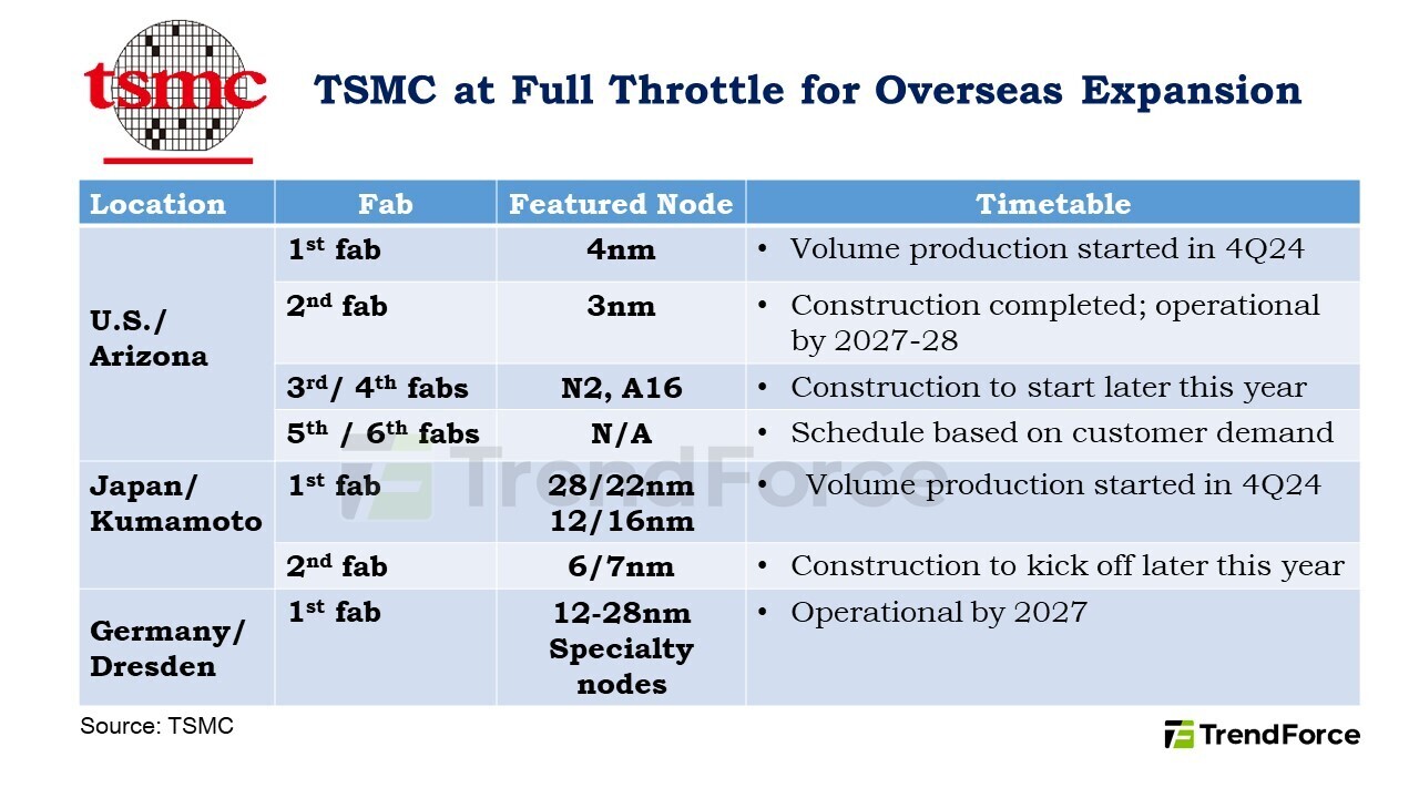
TSMC is speeding up its plans to grow worldwide, the company's Chairman, C.C. Wei is announcing they'll start building their third and fourth fabs in Arizona later this year. This comes after TSMC finished constructing the second Arizona plant while the first fab started volume production in Q4 2024. TSMC wants to open its second factory about six months earlier than planned due to increasing customer demand. The first factory will make 4 nm chips, the second will target 3 nm chips, and the newer ones will work on even smaller N2 and A16 nodes. This rapid expansion is part of TSMC's additional $100 billion investment to build five more semiconductor plants and a research center in the U.S. In total, TSMC will invest $165 billion in the United States.
Besides its US operations, TSMC keeps pushing forward with its worldwide manufacturing plans. Wei dismissed rumors of setbacks at the company's upcoming Kumamoto plant in Japan. He confirmed that their first fab started mass production in late 2024, achieving excellent yields. They plan to begin building a second Japanese facility this year, once the infrastructure is ready. The company's European expansion in Dresden is also on track, with strong backing from both the European Commission and the German federal government. They broke ground at the Dresden site in August 2024 as Europe's first FinFET-capable dedicated foundry operation.

Source:
TrendForce
Besides its US operations, TSMC keeps pushing forward with its worldwide manufacturing plans. Wei dismissed rumors of setbacks at the company's upcoming Kumamoto plant in Japan. He confirmed that their first fab started mass production in late 2024, achieving excellent yields. They plan to begin building a second Japanese facility this year, once the infrastructure is ready. The company's European expansion in Dresden is also on track, with strong backing from both the European Commission and the German federal government. They broke ground at the Dresden site in August 2024 as Europe's first FinFET-capable dedicated foundry operation.
8 Comments on TSMC Expands U.S. Footprint with Two New Fabs in Arizona
For mobile phones and servers/desktops/laptops CPUs/GPUs, I guess maybe in the next millennium...Europe should develop it's own microconductor mega corporations. They had ASML, which is the default monopoly company for tooling. Imagine ASML only selling in Europe ;)
But somebody has to pay for the techno-independence goals, and it sure as hades aint gonna be TSMC.
Even with help from the CHIPS Act funding, us little people will STILL end up paying for the expansion through higher taxes down the road :D
The reason "old" nodes are still being used, is because there are tons of things that don't benefit from node shrinks or that can't be shrunk with current technology.
Analog signalling is one of those, so things like WiFi, Bluetooth, 5G and all that other wireless malarkey has an RF front-end that I believe is still made using 40 nm using standard CMOS tech, but using something like FD-SOI you can go down to 22 nm and there are even RF specific nodes that tend to stick to something like 40 to 22 nm nodes.
But maybe you prefer to plug in a cable to access the internet?