GlobalFoundries Explores UMC Merger to Strengthen Mature Node Manufacturing
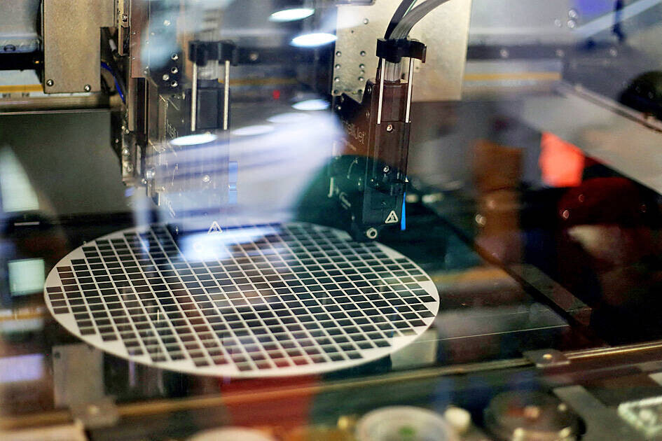
GlobalFoundries is considering acquiring United Microelectronics Corporation (UMC) in a plan called "Project Ultron." The two companies want to work together to make older types of semiconductor nodes. Both companies have moved away from making the newest, most advanced chips. Instead, they focused on making older nodes (28 nm and larger) better and cheaper, keeping them from competing directly with giants like TSMC, Intel, and Samsung. This type of market is mature nodes, which is the main target of automakers and commercial electronics (fridges, washing machines) that aren't CPUs or GPUs, where the latest nodes aren't essential. If GF and UMC merge, they could control about 28% of the mature node market, making them stronger against growing rivals. The possible team-up comes as Chinese companies like SMIC are putting more money into making similar chips, creating more competition.
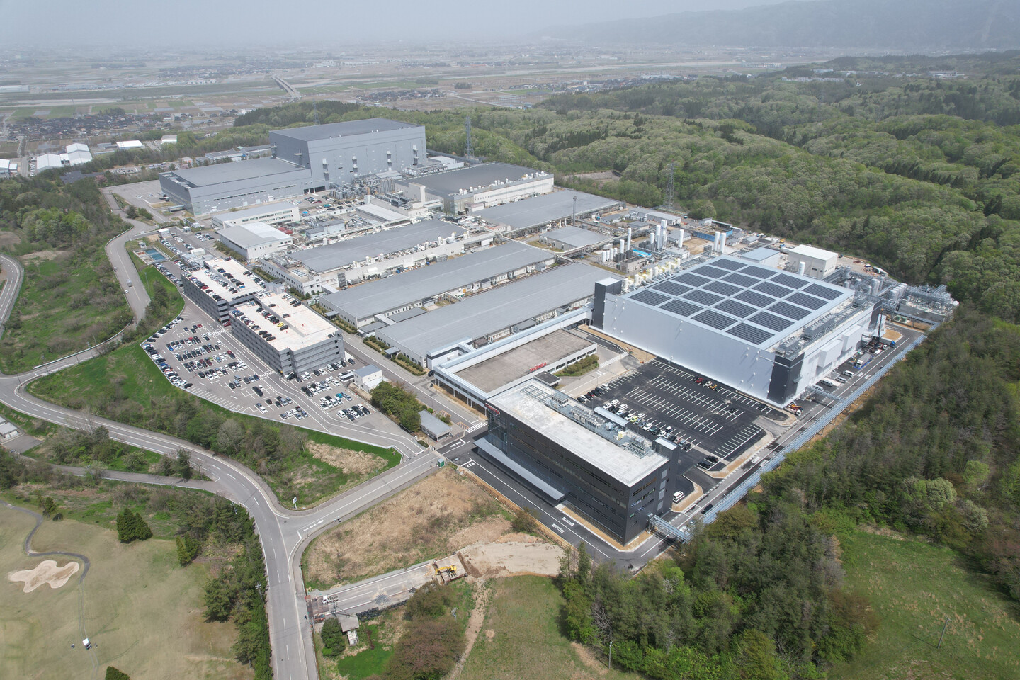
The combined companies would have factories in the United States, Germany, Singapore, Taiwan, and China. Spreading factories across regions could help them keep making chips even if problems happen in one region, be it some tense geopolitical situation or sanctions/tariffs. It might also appeal to customers who worry about supply chain problems. Money issues could make the deal tricky. GlobalFoundries is worth about $20.41 billion but would need to borrow money or get more funding from its main investor, Mubadala, to make the purchase. Government approvals are another big hurdle. Taiwan might not want a foreign company controlling UMC, while China might only approve if the new company promises to keep or add factories in China. UMC has Fab 12X in China, producing 25,000 wafers per month. All of this is happening as GlobalFoundries prepares for new CEO Tim Breen to start by the end of April. He must handle these merger talks while keeping the company running smoothly in a challenging mature node market. Meanwhile, UMC has denied merger talk, but Tom's Hardware claims it has reviewed documents of the merger assessment.
The combined companies would have factories in the United States, Germany, Singapore, Taiwan, and China. Spreading factories across regions could help them keep making chips even if problems happen in one region, be it some tense geopolitical situation or sanctions/tariffs. It might also appeal to customers who worry about supply chain problems. Money issues could make the deal tricky. GlobalFoundries is worth about $20.41 billion but would need to borrow money or get more funding from its main investor, Mubadala, to make the purchase. Government approvals are another big hurdle. Taiwan might not want a foreign company controlling UMC, while China might only approve if the new company promises to keep or add factories in China. UMC has Fab 12X in China, producing 25,000 wafers per month. All of this is happening as GlobalFoundries prepares for new CEO Tim Breen to start by the end of April. He must handle these merger talks while keeping the company running smoothly in a challenging mature node market. Meanwhile, UMC has denied merger talk, but Tom's Hardware claims it has reviewed documents of the merger assessment.