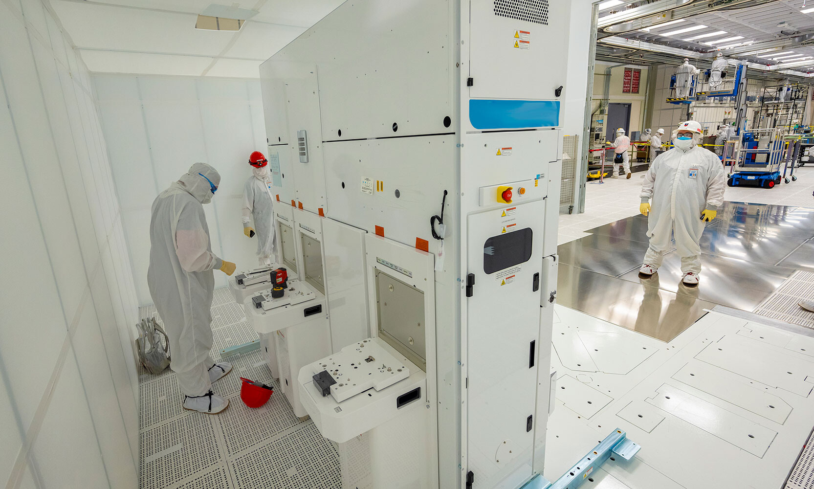
News Posts matching #Fab

Return to Keyword Browsing

Revenue of Top 10 IC Design (Fabless) Companies Reaches US$29.8 Billion for 2Q21, Though Growth May Potentially Slow in 2H21, Says TrendForce

In view of the ongoing production capacity shortage in the semiconductor industry and the resultant price hike of chips, revenue of the top 10 IC design companies for 2Q21 reached US$29.8 billion, a 60.8% YoY increase, according to TrendForce's latest investigations. In particular, Taiwanese companies put up remarkable performances during this period, with both MediaTek and Novatek posting YoY growths of more than 95%. AMD, on the other hand, experienced a nearly 100% YoY revenue growth, the highest among the top 10.

TrendForce indicates that the ranking of the top five companies for 2Q21 remained unchanged from the previous quarter, although there were major changes in the 6th to 10th spots. More specifically, after finalizing its acquisition of Inphi, Marvell experienced a major revenue growth and leapfrogged Xilinx and Realtek in the rankings from 9th place in 1Q21 to 7th place in 2Q21.

TSMC Rumoured to Build New Fab in Southern Taiwan

According to Nikkei, TSMC is set to start building a new fab in Kaohsiung, which is Taiwan's third largest city and located in the south of the island. It's also where ASE Technology Holding is located, which is the world's largest chip packaging and testing contractor. So far, TSMC doesn't have any fabs this far south in Taiwan, but it's not without its challenges.

The new fab is said to be designed to build chips on TSMC's 6 and 7 nm nodes, which are currently their most popular nodes, although this is likely to change as their 5 nm node begins to ramp up production. That said, there will still continue to be a huge demand for 6 and 7 nm parts, as these nodes transition to become mainstream production nodes.

Intel Oregon Fab Expansion Milestone: First Chipmaking Tool Rolls in

For most people, a tool is something you hold in your hand: pliers, hammer, screwdriver. Inside an Intel chip factory, a tool is a whole different deal. Fab tools are huge and hugely costly and take entire teams to muscle into place and install. As Intel aggressively ramps its worldwide manufacturing footprint, a construction milestone recently passed at Intel's Ronler Acres factory in Hillsboro, Oregon.

At the company's massive $3 billion Mod3 factory expansion, the first tool rolled in. The honor went to a thin film deposition tool. It arrived not in a leather tool belt, but aboard two semitractor-trailers. Once completed and hooked up, it will weigh 10 tons. And by the time the Mod3 project is done in about six months, the thin film deposition tool will be joined by more than a dozen like it. A typical Intel fab, once built out, is stuffed with about 1,200 chipmaking tools, many of them costing millions of dollars apiece.

TSMC Under U.S. Pressure Over China Fab Expansion

TSMC is under pressure from the U.S. to reconsider its plans to expand its facilities in mainland China, sources close to the matter told DigiTimes. TSMC currently operates a fab near Shanghai, and one in Nanjing, which it had originally planned to expand, meeting resistance from the U.S. It is not known if this is government (diplomatic) pressure or by U.S. based customers of TSMC., but is likely a combination of the two. The same forces were possibly behind getting TSMC to invest north of $3.5 billion toward a facility in Arizona with six more "Gigafabs" being planned in the southwestern state. U.S. hand-holding in TSMC's policymaking could be part of a strategy to deny cutting-edge silicon fabrication technology to China (PRC), and to help TSMC expand its manufacturing in safer regions as the security situation across the Taiwan strait continues to deteriorate. TSMC, specifically western tech companies' dependence on it, makes it a soft target on the island, and a bargaining chip to deter western military intervention.

Micron to Sell Lehi, Utah, Fab to Texas Instruments

Micron Technology, Inc. announced today that it has entered into a definitive agreement to sell its Lehi, Utah, fab to Texas Instruments. The economic value for Micron from the sale is $1.5 billion, comprised of $900 million in cash from TI from the sales transaction, and approximately $600 million in value from select tools and other assets. Micron has sold some of these assets and will retain the remainder to redeploy to its other manufacturing sites or sell to other buyers.

Micron's Lehi, Utah, facility has been home to a highly skilled team with expertise in all aspects of advanced semiconductor manufacturing. TI will offer all Lehi site team members the opportunity to become employees upon the closing of the sale and intends to deploy its own technologies at the site. The sale is anticipated to close later this calendar year.

"Micron's Lehi, Utah, facility has a strong history of technology innovation and leading-edge semiconductor manufacturing," said Micron President and CEO, Sanjay Mehrotra. "We are pleased to have reached an agreement with Texas Instruments as it is an industry leader and truly values the talented Lehi team and the capabilities this site offers to deploy its technology effectively. We are greatly appreciative of the contributions that the Lehi team has made to Micron, as well as the collaboration and engagement Micron has had with the local community."

Raytheon Technologies and GLOBALFOUNDRIES Partner to Accelerate 5G Wireless Connectivity Using Gallium Nitride on Silicon (GaN-on-Si)

Raytheon Technologies (NYSE: RTX), a leading aerospace and defense technology company, and GLOBALFOUNDRIES (GF ), the global leader in feature-rich semiconductor manufacturing, will collaborate to develop and commercialize a new gallium nitride on silicon (GaN-on-Si) semiconductor that will enable game-changing radio frequency performance for 5G and 6G mobile and wireless infrastructure applications.

Under the agreement, Raytheon Technologies will license its proprietary gallium nitride on silicon technology and technical expertise to GF, which will develop the new semiconductor at its Fab 9 facility in Burlington, Vermont. Gallium nitride is a unique material used to build high-performance semiconductors that can handle significant heat and power levels. This makes it ideal to handle 5G and 6G wireless signals, which require higher performance levels than legacy wireless systems.

Revenue of Top 10 IC Design (Fabless) Companies for 2020 Undergoes 26.4% Increase YoY, Says TrendForce

The emergence of the COVID-19 pandemic in 1H20 seemed at first poised to devastate the IC design industry. However, as WFH and distance education became the norm, TrendForce finds that the demand for notebook computers and networking products also spiked in response, in turn driving manufacturers to massively ramp up their procurement activities for components. Fabless IC design companies that supply such components therefore benefitted greatly from manufacturers' procurement demand, and the IC design industry underwent tremendous growth in 2020. In particular, the top three IC design companies (Qualcomm, Broadcom, and Nvidia) all posted YoY increases in their revenues, with Nvidia registering the most impressive growth, at a staggering 52.2% increase YoY, the highest among the top 10 companies.

GLOBALFOUNDRIES 22FDX RF Solution Provides the Basis for Next-Gen mmWave Automotive Radar

GLOBALFOUNDRIES (GF ), the global leader in specialty semiconductor manufacturing, and Bosch will partner to develop and manufacture next-generation automotive radar technology.

Bosch chose GF as its partner to develop a mmWave automotive radar system-on-chip (SoC) for Advanced Driver Assistance Systems (ADAS) applications, manufactured using GF's 22FDX RF solution. ADAS applications help drivers stay safe by keeping a vehicle in the correct lane, warning of collisions, initiating emergency braking, assisting with parking, and more.

TSMC Could Build Six GigaFabs in Arizona

Taiwan Semiconductor Manufacturing Company (TSMC), one of the largest manufacturers of silicon, is seemingly making plans to build as many as six of its US-based fabs in Arizona. According to the unconfirmed report coming from UDN, TSMC could be building its Arizona-based factories for much larger capacities. Based on TSMC's classifications, the MegaFab-class of factories is the one with 25,000 WSPM output. According to the report, TSMC plans to build six additional facilities in the area where the Arizona fab is, and have a GigaFab-class (even larger type) factory present on US soil. Currently, the company operates six GigaFabs and all of them are based in Taiwan.

The GigaFab class factory is supposed to have over 100,000 WSPM output, and by building one in the US, TSMC could get much closer to big customers like Apple, NVIDIA, and AMD. Reports are saying that TSMC's primary target is 3 nm node production on 12-inch (300 mm) wafers. All six of the supposed facilities are expected to output more than 100,000 wafers at their peak, making it one of the largest projects TSMC has ever done. The Arizona location is supposed to serve as a "mega fab" facility and it is supposed to start manufacturing silicon in 2024. This information is, of course, just a rumor so you should take it with a grain of salt, as this type of information is usually only known by top-level management.

Intel CEO Says Using Competitor's Semiconductor Process in Intel Fabs is an Option

Semiconductor manufacturing is not an easy feat to achieve. Especially if you are constantly chasing the smaller and smaller node. Intel knows this the best. The company has had a smooth transition from other nodes to the smaller ones until the 10 nm node came up. It has brought Intel years of additional delay and tons of cost improving the yields of a node that was seeming broken. Yesterday the company announced the new Tiger Lake-H processors for laptops that are built using the 10 nm process, however, we are questioning whatever Intel can keep up with the semiconductor industry and deliver the newest nodes on time, and with ease. During an interview with Intel's CEO Bob Swan, we can get a glimpse of Intel's plans for the future of semiconductors at the company.

In the interview, Mr. Swan has spoken about the technical side of Intel and how the company plans to utilize its Fabs. The first question everyone was wondering was about the state of 10 nm. The node is doing well as three Fabs are ramping up capacity every day, and more products are expected to arrive on that node. Mr. Swan has also talked about outsourcing chip production, to which he responded by outlining the advantage Intel has with its Fabs. He said that outsourcing is what is giving us shortages like AMD and NVIDIA experience, and Intel had much less problems. Additionally, Mr. Swan was asked about the feasibility of new node development. To that, he responded that there is a possibility that Intel could license its competitor's node and produce it in their Fabs.

NAND Flash Revenue for 3Q20 up by Only 0.3% QoQ Owing to Weak Server Sales, Says TrendForce

Total NAND Flash revenue reached US$14.5 billion in 3Q20, a 0.3% increase QoQ, while total NAND Flash bit shipment rose by 9% QoQ, but the ASP fell by 9% QoQ, according to TrendForce's latest investigations. The market situation in 3Q20 can be attributed to the rising demand from the consumer electronics end as well as the recovering smartphone demand before the year-end peak sales season. Notably, in the PC market, the rise of distance education contributed to the growing number and scale of Chromebook tenders, but the increase in the demand for Chromebook devices has not led to a significant increase in NAND Flash consumption because storage capacity is rather limited for this kind of notebook computer. Moreover, clients in the server and data center segments had aggressively stocked up on components and server barebones during 2Q20 due to worries about the impact of the pandemic on the supply chain. Hence, their inventories reached a fairly high level by 3Q20. Clients are now under pressure to control and reduce their inventories during this second half of the year. With them scaling back procurement, the overall NAND Flash demand has also weakened, leading to a downward turn in the contract prices of most NAND Flash products.

TSMC Completes Its Latest 3 nm Factory, Mass Production in 2022

They say that it is hard to keep up with Moore's Law, however, for the folks over at Taiwan Semiconductor Manufacturing Company (TSMC), that doesn't seem to represent any kind of a problem. Today, to confirm that TSMC is one of the last warriors for the life of Moore's Law, we have information that the company has completed building its manufacturing facility for the next-generation 3 nm semiconductor node. Located in Southern Taiwan Science Park near Tainan, TSMC is expecting to start high-volume manufacturing of the 3 nm node in that Fab in the second half of 2022. As always, one of the first customers expected is Apple.

Estimated to cost an amazing 19.5 billion US Dollars, the Fab is expected to have an output of 55,000 300 mm (12-inch) wafers per month. Given that the regular facilities of TSMC exceed the capacity of over 100K wafers per month, this new facility is expected to increase the capacity over time and possibly reach the 100K level. The new 3 nm node is going to use the FinFET technology and will deliver a 15% performance gain over the previous 5 nm node, with 30% decreased power use and up to 70% density increase. Of course, all of those factors will depend on a specific design.

Raja Koduri to Present at Samsung Foundry Forum amid Intel's Outsourcing Efforts

Intel's chief architect and senior vice president of discrete graphics division, Mr. Raja Koduri, is said to be scheduled to present at Samsung Electronics Event day. With a presentation titled "1000X More Compute for AI by 2025", the event is called Samsung Foundry SAFE Forum. It is a global virtual conference designed to be available to everyone. So you might be wondering what is Mr. Koduri doing there. Unless you have been living under a rock, you know about Intel's struggles with node manufacturing. Specifically, the 10 nm node delays that show the company's efforts to deliver a node on time. The same is happening with the 7 nm node that also experienced significant delays.

Intel has a contract to develop an exascale supercomputer at Argonne National Laboratory, called Aurora. That supercomputer is using Intel's CPUs and the company's upcoming Xe GPUs. Since the company has problems with manufacturing and has to deliver the products (it is bound by several contracts) to its contractors and customers, it decided to look at external manufacturers for its products, specifically Xe graphics. Being that Mr. Koduri tweeted an image of him visiting Samsung Giheung Fab in Korea, and now presenting at the Samsung Foundry event, it is possible that Intel will tap Samsung's semiconductor manufacturing process for its Xe GPU efforts and that Samsung will be the contractor in charge.

China Forecast to Represent 22% of the Foundry Market in 2020, says IC Insights

IC Insights recently released its September Update to the 2020 McClean Report that presented the second of a two-part analysis on the global IC foundry industry and included a look at the pure-play foundry market by region.

China was responsible for essentially all of the total pure-play foundry market increase in 2018. In 2019, the U.S./China trade war slowed China's economic growth but its foundry marketshare still increased by two percentage points to 21%. Moreover, despite the Covid-19 shutdown of China's economy earlier this year, China's share of the pure-play foundry market is forecast to be 22% in 2020, 17 percentage points greater than it registered in 2010 (Figure 1).

NXP Advances 5G with New Gallium Nitride Fab in Arizona

NXP Semiconductors N.V. today announced the grand opening of its 150 mm (6-inch) RF Gallium Nitride (GaN) fab in Chandler, Arizona, the most advanced fab dedicated to 5G RF power amplifiers in the United States. The new internal factory combines NXP's expertise as the industry leader in RF power and its high-volume manufacturing know-how, resulting in streamlined innovation that supports the expansion of 5G base stations and advanced communication infrastructure in the industrial, aerospace and defense markets.

COVID-19 Drives Rise in Global Fab Equipment Spending, SEMI Reports

Soaring pandemic-inspired demand for chips that power everything from communications and IT infrastructures to personal computing, gaming and healthcare electronics will drive an 8% increase in global fab equipment spending in 2020 and a 13% increase in 2021, SEMI announced today in its World Fab Forecast report. Rising demand for semiconductors for datacenter infrastructures and server storage along with the buildup of safety stock as U.S.-China trade tensions intensify are also contributing to this year's growth.

The bullish trend for overall fab equipment investments comes as the semiconductor industry recovers from a 9% decline in fab spending in 2019 and navigates a roller-coaster 2020 with actual and projected spending drops in the first and third quarters mixed with second- and fourth-quarter increases. See figure below:

GLOBALFOUNDRIES Announces 12LP+ Enhanced 12nm Silicon Fabrication Node

GLOBALFOUNDRIES (GF), the world's leading specialty foundry, today announced its most advanced FinFET solution, 12LP+, has completed technology qualification and is ready for production. GF's differentiated 12LP+ solution is optimized for artificial intelligence (AI) training and inference applications. Built on a proven platform with a robust production ecosystem, 12LP+ offers chip designers an efficient development experience and a fast time-to-market.

Contributing to its best-in-class combination of performance, power and area, 12LP+ introduces new features including an updated standard cell library, an interposer for 2.5D packaging, and a low-power 0.5 V Vmin SRAM bitcell that supports the low latency and power-efficient shuttling of data between the AI processors and memory. The result is a semiconductor solution engineered to meet the specific needs of the fast-growing AI market.

Semiconductor Fabs to Log Record Spending of Nearly $68 Billion in 2021, SEMI Reports

2021 is poised to mark a banner year for global fab equipment spending with 24 percent growth to a record US$67.7 billion, 10 percent higher than the previously forecast US$65.7 billion, and all product segments promising solid growth rates, according to the second-quarter 2020 update of the SEMI World Fab Forecast report. Memory fabs will lead worldwide semiconductor segments with US$30 billion in equipment spending, while leading-edge logic and foundry is expected to rank second with US$29 billion in investments.

The 3D NAND memory subsegment will help power the spending spree with a 30 percent jump in investments this year before tacking on 17 percent growth in 2021. DRAM fab investments will surge 50 percent next year after declining 11 percent in 2020, and fab spending on logic and foundry, mainly leading edge, will trace a similar but more muted trajectory, rising 16 percent 2021 after an 11 percent drop this year.

TSMC Says it Still Won't Build a Fab in the US

TSMC, as one of the largest silicon manufacturers in the world, has been subject to pressure from the Trump administration to build a Fab and manufacture silicon on US soil. The reasoning behind this is that the US government could order chips that are supposed to be used in military applications. For security reasons, they need to be manufactured on US grounds and "checked" by the US government. However, it seems like a Taiwanese company has no concrete plans to realize the building of the US Fab.

Thanks to the report of DigiTimes, TSMC has confirmed that they have resisted requests from the US government, and will not build a Fab on US soil for the government. They haven't dismissed the possibility of building one or silicon manufacturing facilities in the US completely. TSMC chairman Mark Liu has told DigiTimes previously that if the company wants to build a US Fab, it will do so because of consumer demand, not the government demand. And that is understandable. It is much easier to work with regular customers compared to the US government which would force a company to go through rigorous security levels to deliver chips.
TSMC HQ

TSMC Sets Aside Almost 7 Billion Dollars for Fab Expansion

TSMC is working hard to ensure its number one spot in the semiconductor manufacturing industry, and it has the funds to back it up. Yesterday TSMC's Board of Directors approved the company budget for another semiconductor fab expansion. With a budget totaling 6.74 billion US dollars allocated, TSMC has "Approved capital appropriations of approximately US$6,742.1 million (approximately NT$200.9 billion) for purposes including: 1) Fab construction, and installation of fab facility systems; 2) Installation and upgrade of advanced technology capacity; 3) Installation of specialty technology capacity; 4) Installation of advanced packaging capacity; 5) Second quarter 2020 R&D capital investments and sustaining capital expenditures."

TSMC Begins 3 nm Fab Construction

TSMC has been very aggressive with its approach to silicon manufacturing, with more investments into its R&D that now match or beat the capex investments of Intel. That indicates a strong demand for new technologies and TSMC's strong will not drop out of the never-ending race for more performance and smaller node sizes.

According to the sources over at DigiTimes, TSMC has acquired as much as 30 hectares of land in the Southern Taiwan Science Park to begin the construction of its fabs that are supposed to start high-volume manufacturing 3 nm node in 2023. Construction of 3 nm manufacturing facilities are set to begin in 2020 when TSMC will lay the groundwork for the new fab. The 3 nm semiconductor node is expected to be TSMC's third attempt at EUV lithography, right after the 7 nm+, and 5 nm nodes which are also based on EUV technology.

GLOBALFOUNDRIES Introduces 12LP+ FinFET Solution for Cloud and Edge AI Applications

GLOBALFOUNDRIES (GF), the world's leading specialty foundry, announced today at its Global Technology Conference the availability of 12LP+, an innovative new solution for AI training and inference applications. 12LP+ offers chip designers a best-in-class combination of performance, power and area, along with a set of key new features, a mature design and production ecosystem, cost-efficient development and fast time-to-market for high-growth cloud and edge AI applications.

Derived from GF's existing 12nm Leading Performance (12LP) platform, GF's new 12LP+ provides either a 20% increase in performance or a 40% reduction in power requirements over the base 12LP platform, plus a 15% improvement in logic area scaling. A key feature is a high-speed, low-power 0.5 V SRAM bit cell that supports the fast, power-efficient shuttling of data between processors and memory, an important requirement for AI applications in the computing and wired infrastructure markets.

Intel Invests €7 Billion in Ireland Toward a New Fab

Intel is following up on its massive $11 billion investment in Israel with a second large manufacturing investment, this time in Leixlip, Ireland. The company has earmarked a €7 billion investment toward construction of a new fab in Leixlip, which will employ 1,600 people, and have a built-up area of 110,000 m². This fab will sit alongside existing fabs that already employ over 4,500 staff. The company did not go into details of what the fab will manufacture. The investment aligns with Intel's strategy of massive investments in manufacturing to increase its chip volumes as enterprises, small and medium businesses, and consumers at large look to upgrade their computers at the turn of the decade. The company is already combating acute shortages of processors in the retail channel.

TSMC's 7 nm Fabrication Becomes Biggest Share of Revenue in 4Q18

TSMC's introduction of its 7 nm fabrication technology has essentially propelled the company to silicon manufacturing heights. Every company - particularly in the mobile space - is after the most minute increase in transistor density and power consumption improvements the latest and greatest can bring. AMD themselves have become a major TSMC partner in pursuit of its newfound competitiveness against Intel, and has apparently leveraged the 7 nm process as a way to keep its high-performance GPU offering minimally competitive with NVIDIA's solution - at a much lesser die area requirement, if the Radeon VII vs RTX 2080 estimates are something to go by.

As a consequence of the market interest for the 7 nm process, it has rapidly become TSMC's biggest revenue generator as soon as 4Q18. The company said that 7 nm already generated 10% of the company's entire 2018 revenue, despite the process only having been ramped up in June of the same year. Other less dense technologies still generate a lot of revenue for the company, and are likely much higher volume. However, TSMC is most likely riding on much increased ASP for 7 nm wafers than for other technologies.

Samsung, SK Hynix Slowing Down NAND, DRAM Fab Expansion Plans in Wake of Lower Demand Projections

DigiTimes is reporting plans from both Samsung and SK Hynix to slow down their fabrication capacity expansion plans for NAND and DRAM in wake of lower than expected demand projection for the first half of 2019. This move comes at a time where DRM pricing is still extremely prohibitive due to "higher demand than fabrication capacity output" - and we'd already seen the companies base their fabrication expansions on lower than expected demand increases, as a way to artificially keep pricing for the memory commodity high. NAND is another case - price per GB has been dropping like a rock. And now, the companies want to thwart expected lower demand with lower production values.

Samsung, for one, has reportedly put its plans for additional new production capacity for 1ynm DRAM chips at its fabs in Hwaseong and Pyeongtaek on hold. The chip vendor previously planned to build an additional 30,000 wafers monthly for DRAM memory starting the third quarter of 2018, the sources said - but is now looking to reduce that number to keep pricing from bottoming out. Sk Hynix is also reported to have slowed down its projected production, but details are scarcer on that side of the fence. All in all, it seems that whether there is demand or not, seeing DRAM prices falling to their previous levels is a dream in both name and, not paradoxically, reality.
Return to Keyword Browsing
Oct 18th, 2024 04:59 EDT change timezone

New Forum Posts

Popular Reviews

Controversial News Posts