News Posts matching #FinFET

Return to Keyword Browsing

Cadence Accelerates SoC, 3D-IC and Chiplet Design for AI Data Centers, Automotive and Connectivity in Collaboration with Samsung Foundry

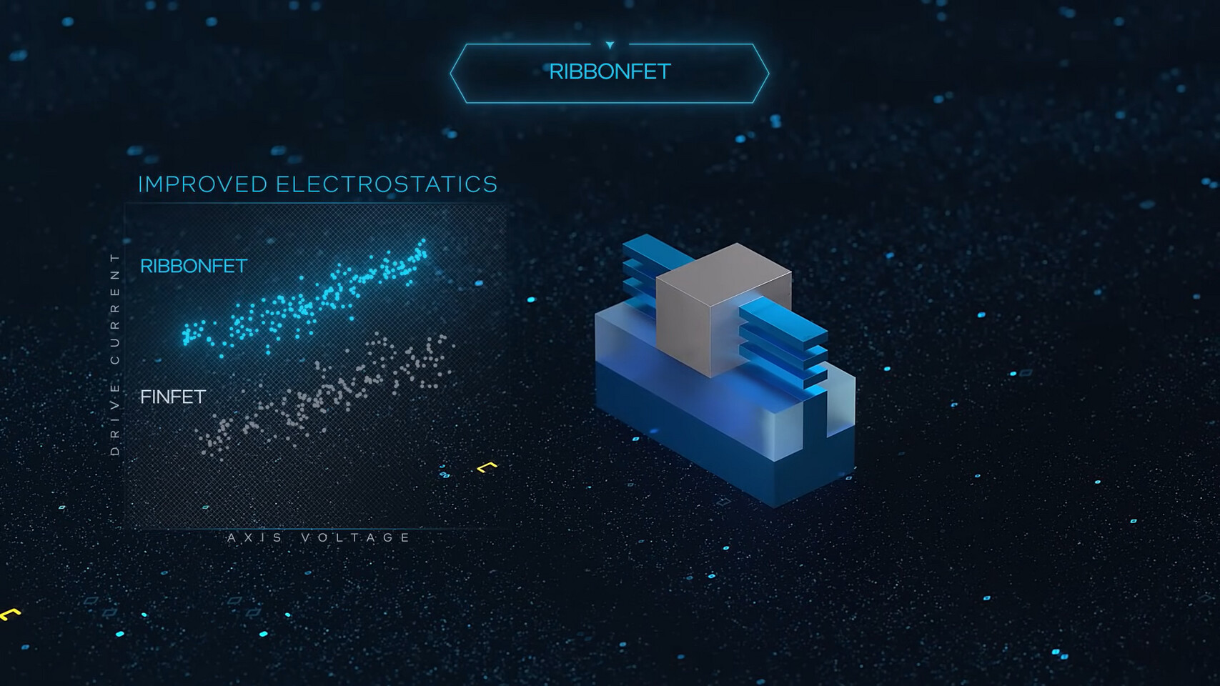
Cadence today announced an expansion of its collaboration with Samsung Foundry, including a new multi-year IP agreement to broaden Cadence memory and interface IP solutions in Samsung Foundry's SF4X, SF5A and SF2P advanced process nodes. Furthering their ongoing technology collaboration, the companies are leveraging Cadence's AI-driven design solutions and Samsung's advanced SF4X, SF4U and SF2P process nodes to deliver high-performance, low-power solutions for AI data center, automotive—including advanced driver-assistance systems (ADAS)—and next-generation RF connectivity applications.

Cadence's AI-driven design solutions and comprehensive portfolio of IP and silicon solutions enhance designers' productivity and accelerate time to market (TTM) for leading-edge SoCs, chiplets and 3D-ICs on advanced Samsung Foundry processes. "We support a full portfolio of IP, subsystems and chiplets on the Samsung Foundry process nodes, and our latest multi-year IP agreement strengthens our ongoing collaboration," said Boyd Phelps, senior vice president and general manager of the Silicon Solutions Group at Cadence. "By combining Cadence's AI-driven design and silicon solutions with Samsung's advanced processes, we're delivering the leading-edge technologies our mutual customers need to innovate and bring their products to market faster."

Client Interest in Samsung Foundry Reportedly Buoyed by Nintendo Switch 2 SoC Production Deal

The Nintendo Switch 2 hybrid console is due to launch globally next Wednesday (June 4). The highly anticipated next-gen handheld is powered by a custom NVIDIA processor. To the surprise of many industry watchdogs, both parties have semi-recently disclosed a couple of technical details regarding their fruitful hardware collaboration. Historically, Nintendo has guarded many aspects of its past generation hardware. Throughout the 2020s, data miners and leakers have unearthed plenty of pre-release information—leading to theories about the Switch 2 chipset's origins. During the Switch 1 era, TSMC was the chosen manufacturing partner. NVIDIA's off-the-shelf Tegra X1 mobile SoC powered the first wave of Nintendo Switch (2017) devices, in 20 nm form. A 2019 revision resulted in Switch Lite and (refreshed) Switch models being equipped with a more efficient 16 nm solution, also present within 2023's premium OLED variant.

Since then, Switch 2's alleged NVIDIA Tegra T239 SoC was linked to a Samsung 8 nm node process. Earlier this month, extremely brave Chinese leakers produced "full die shot" evidence of South Korean foundry origins. Bloomberg insider news articles have implied that Samsung Semi's mature 8 nm FinFET node is better suited—rather than an equivalent TSMC product—for the Switch 2's custom NVIDIA chipset. Unnamed sources have mentioned critical factors; namely stable production and process compatibility. Industry moles reckon that Samsung leadership is actively and aggressively pushing for a longer Switch 2 chipset production deal. Renewed terms could include a future die shrink; pre-launch analysis indicates a sizeable 207 mm² footprint. Beyond foundry biz negotiations, additional murmurs suggest company executives dangling an OLED panel supply agreement. Industry experts have viewed Samsung's key entry—into the gaming console chip market—as a seismic development. A DigiTimes article dives into a so-called "tripartite cooperation"—involving Nintendo, NVIDIA, and the South Korean semiconductor giant. The Samsung Foundry has floundered and struggled in recent times, but is keen to catch up with its arch rival. Fresh rumors have AMD and Sony considering Samsung's chip making channels; possibly with futuristic PlayStation hardware in mind.

Inside "Arrow Lake": Intel's Die Exposed and Annotated

Die shots of Intel's "Arrow Lake" desktop processors have appeared online, confirming the chiplet design we have known about since the launch. The images annotated by the YouTube channel HighYield show a four‑tile arrangement mounted on a base die made with Intel's 22 nm FinFET process. The compute tile sits at the top left, built on TSMC's N3B node and covering 117.24 mm². To its right are the SoC tile on TSMC's N6 node measuring 86.65 mm², and the GPU tile, which houses four Xe cores alongside an Arc Alchemist render slice. The I/O tile, at 24.48 mm² on the same N6 node, completes the group at the bottom left. Intel has redesigned its hybrid core layout for Arrow Lake, moving away from separate P‑core and E‑core clusters. Four of the eight high‑performance P‑cores line the die's outer edges, with the remaining four in the center. In between these lie the four efficiency E‑core clusters, each sharing 3 MB of L2 cache. A unified 36 MB L3 cache ring bus connects to every core, allowing E‑cores to tap into that larger cache pool for the first time. Intel aims to spread heat more evenly and boost background task performance.

The I/O tile integrates Thunderbolt 4 controllers, PCIe buffers and PHYs. The SoC tile carries display engines, media accelerators and DDR5 memory controllers. All tiles are bonded to the base die via Intel's Foveros Omni stacking technology. Arrow Lake also reflects a shift in Intel's manufacturing strategy. Plans to use Intel's 20A node were dropped in favor of TSMC processes, making this the first desktop CPU from Intel that relies almost entirely on external foundries. On the software side, Intel has begun offering its IPO profiles in select prebuilt systems. These presets optimize CPU and memory settings for a hassle‑free performance boost that remains within warranty limits. Meanwhile, the native 200S Boost overclocking option is rolling out via BIOS updates. Early tests suggest that 200S Boost alone yields modest gains unless paired with very high-speed DDR5 modules, while IPO profiles deliver more consistent improvements with mainstream memory configurations.

TSMC Expands U.S. Footprint with Two New Fabs in Arizona

TSMC is speeding up its plans to grow worldwide, the company's Chairman, C.C. Wei is announcing they'll start building their third and fourth fabs in Arizona later this year. This comes after TSMC finished constructing the second Arizona plant while the first fab started volume production in Q4 2024. TSMC wants to open its second factory about six months earlier than planned due to increasing customer demand. The first factory will make 4 nm chips, the second will target 3 nm chips, and the newer ones will work on even smaller N2 and A16 nodes. This rapid expansion is part of TSMC's additional $100 billion investment to build five more semiconductor plants and a research center in the U.S. In total, TSMC will invest $165 billion in the United States.

Besides its US operations, TSMC keeps pushing forward with its worldwide manufacturing plans. Wei dismissed rumors of setbacks at the company's upcoming Kumamoto plant in Japan. He confirmed that their first fab started mass production in late 2024, achieving excellent yields. They plan to begin building a second Japanese facility this year, once the infrastructure is ready. The company's European expansion in Dresden is also on track, with strong backing from both the European Commission and the German federal government. They broke ground at the Dresden site in August 2024 as Europe's first FinFET-capable dedicated foundry operation.

Intel 18A Is Officially Ready for Customer Projects

Intel has updated its 18A node website with the message, "Intel 18A is now ready for customer projects with the tape outs beginning in the first half of 2025: contact us for more information." The contact hyperlink includes an email where future customers can direct their questions to Intel. Designed as a turnaround node for Intel, 18A carries industry-leading features like SRAM density scaling comparable with TSMC's N2, 15% better performance per watt, and 30% better chip density vs. the Intel 3 process node used in Intel Xeon 6, as well as PowerVia backside-power delivery to increase transistor density.

Other features like RibbonFET are the first to replace FinFET transistors, making gate leakage a tighter control. Interestingly, Intel's first products to use the 18A node are client CPUs "Panther Lake" and "Clearwater Forest" Xeon CPUs for data centers. External Intel Foundry customers using the 18A node include Amazon's AWS, Microsoft for its internal silicon for Azure, and Broadcom exploring 18A-based designs. The process of gaining customers for advanced manufacturing is complex, as many existing Samsung/TSMC customers are not risking their capacity and contracts with established advanced silicon makers. However, if Intel's first few customers prove successful, many others could flock over to Intel's fabs as geopolitical tensions are questioning whether the current models of the semiconductor supply chain are feasible in the future. If US companies and startups decide to move with Intel for their chip manufacturing, Intel could experience a complete recovery.

Intel Foundry Adds New Customers to RAMP-C Project for US Defense

Intel Foundry has announced the onboarding of new defense industrial base (DIB) customers, Trusted Semiconductor Solutions and Reliable MicroSystems, as part of the third phase of the Rapid Assured Microelectronics Prototypes - Commercial (RAMP-C) efforts under the Trusted & Assured Microelectronics (T&AM) Program in the Office of the Under Secretary of Defense for Research and Engineering (OUSD (R&E)). The RAMP-C project, awarded through the Strategic & Spectrum Missions Advanced Resilient Trusted Systems (S²MARTS) Other Transaction Authority (OTA), allows DIB customers to take advantage of Intel Foundry's leading-edge Intel 18A process technology and advanced packaging for prototypes and high-volume manufacturing of commercial and DIB products for the U.S. Department of Defense (DoD).

"We are very excited to welcome Trusted Semiconductor Solutions and Reliable MicroSystems to the RAMP-C project we are engaged in with the DoD. The collaboration will drive cutting-edge, secure semiconductor solutions essential for our nation's security, economic growth and technological leadership. We are proud of the pivotal role Intel Foundry plays in supporting U.S. national defense and look forward to working closely with our newest DIB customers to enable their innovations with our leading-edge Intel 18A technology," said Kapil Wadhera, vice president of Intel Foundry and general manager of Aerospace, Defense and Government Business Group.

Lattice Advances Low Power FPGA Leadership with New Small and Mid-range FPGA Offerings

Today, at Lattice Developers Conference 2024, Lattice Semiconductor expanded its edge to cloud FPGA innovation leadership with the launch of exciting new hardware and software solutions. The new Lattice Nexus 2 next-gen small FPGA platform and the first device family based on the platform, Lattice Certus -N2 general purpose FPGAs, offer advanced connectivity, optimized power and performance, and class-leading security. Lattice also announced new mid-range FPGA device capacity options - Lattice Avant 30 and Avant 50 - and new versions of Lattice design software tools and application-specific solution stacks to help accelerate customer time-to-market.

"At Lattice, we are proud to lead technological advancements in low power, small form factor FPGAs, ensuring our customers have the optimal devices, tools, and solutions to design groundbreaking applications that are power efficient, fast, and secure," said Esam Elashmawi, Chief Strategy and Marketing Officer, Lattice Semiconductor. "From the edge to the cloud across a variety of industries, FPGAs stand at the forefront of innovation, and we're committed to delivering versatile and robust small and mid-range FPGA solutions that enable our customers and partners to unlock their full potential."

TSMC Boosts 2 nm Yields by 6%, Passing Savings to Customers

Being the leading-edge semiconductor manufacturing company, TSMC actively works on increasing the efficiency of its upcoming nodes, even when they are finalized and ready for high-volume manufacturing. According to a TSMC employee identified as Dr. Kim on X, recent test runs of the 2 nm N2 nodes show a 6% improvement in production yields compared to baseline expectations. This advancement could translate into substantial cost savings for the company's customers when mass production begins in late 2025. However, specific details about whether the gains were achieved in SRAM or logic test chips remain undisclosed. The timing is particularly noteworthy as TSMC prepares to launch its shuttle test wafer services for 2 nm technology in January. The N2 process represents a giant leap for TSMC, marking its first gate-all-around (GAA) nanosheet transistors implementation, the first step to derive from the classical FinFET design.

According to TSMC's projections, chips manufactured using the N2 process will consume 25-30% less power while maintaining the same transistor count and frequency as its N3E node. Additionally, the technology is expected to deliver 10-15% performance improvements and achieve a 15% increase in transistor density. A key innovation in the N2 process is the enhanced design of its GAA nanosheet transistors, which offers improved electrostatic control and reduced gate leakage compared to 3 nm FinFET transistors, given that the gate can be controlled from all sides. This advancement enables smaller high-density transistors to maintain reliable performance through better threshold voltage tuning capabilities. With approximately seven to eight months until full-scale volume production begins, the company has a substantial window to optimize the manufacturing process further and potentially achieve additional yield improvements, although that is less likely.

Intel and Samsung to Form "Foundry Alliance" to Compete With TSMC, Notes Report

Last time we reported on Samsung Foundry, the company publicly apologized for its setbacks in the memory and foundry divisions, especially as its 3 nm GAA FET node has failed to attract new customers. On the other hand, Intel has also been struggling with its Foundry unit bleeding billions of Dollars in a bid to secure its spot as one of the best foundries for companies to manufacture their chips. There is no better pair than two struggling foundries looking for customers and new ways to conduct research than Intel and Samsung. According to an exclusive by South Korean media outlet "MK," it has reportedly been confirmed that Intel approached Samsung to form a "Foundry Alliance" to boost their foundry business units.

According to the source, Intel CEO Pat Gelsinger is reportedly eager to meet with Samsung Electronics Chairman Lee Jae-yong face-to-face to discuss "comprehensive collaboration in the foundry sector." What exactly will happen between the two is still unclear. Back in 2014, GlobalFoundries and Samsung formed a partnership for 14 nm FinFET offerings, and that was a wide success. Jointly developing a node and offering it in their foundry units could be the target goal for Intel and Samsung. At some level, research and development, as well as sharing valuable manufacturing information on yield improvements, should be beneficial for both to put together the final pieces of the semiconductor puzzle.

TSMC Rumoured to Start Construction on German Fab Within the Next Few Weeks

After many back and forths, it now appears that TSMC is finally getting ready to start construction of its fab in Dresden, Germany. Multiple news outlets are reporting that TSMC is getting ready to start production on its new fab within the next few weeks, which is ahead of the expected Q4 groundbreaking. That said, TSMC has yet to announce an official date for a groundbreaking ceremony or a date when construction will start, but according to media reports TSMC's Chairman and CEO C.C. Wei will be in Germany at the end of August to sign documents with the German government and during this trip, the groundbreaking ceremony is expected to take place.

Assuming everything goes according to plan, the Dresden fab is expected to start production sometime in late 2027, but it's far from a cutting edge fab, as it'll mainly be supplying the European automotive industry with components. The new fab should start its life with two different process technologies, namely a 28 or 22 nm planar CMOS node as well as a 16 or 12 nm FinFET node. The Dresden fab is said to have a production capacity of around 40,000 12-inch wafers monthly. The new fab is expected to be an investment in excess of €10 billion for TSMC, with the city of Dresden spending an additional €250 million for a special water supply system and enhancements to the power grid. Unlike similar projects, TSMC will not be the sole owner of the new fab, as Infineon, Robert Bosch and NXP are each taking a 10 percent stake in the fab.

TSMC Begins 3 nm Production for Intel's "Lunar Lake" and "Arrow Lake" Tiles

TSMC has commenced mass-production of chips for Intel on its 3 nm EUV FinFET foundry node, according to a report by Taiwan industry observer DigiTimes. Intel is using the TSMC 3 nm node for the compute tile of its upcoming Core Ultra 300 "Lunar Lake" processor. The company went into depth about "Lunar Lake" in its Computex 2024 presentation. While a disaggregated chiplet-based processor like "Meteor Lake," the new "Lunar Lake" chip sees the CPU cores, iGPU, NPU, and memory controllers sit on a single chiplet called the compute tile, built on the 3 nm node; while the SoC and I/O components are disaggregated the chip's only other chiplet, the SoC tile, which is built on the TSMC 6 nm node.

Intel hasn't gone into the nuts and bolts of "Arrow Lake," besides mentioning that the processor will feature the same "Lion Cove" P-cores and "Skymont" E-cores as "Lunar Lake," albeit arranged in a more familiar ringbus configuration, where the E-core clusters share L3 cache with the P-cores (something that doesn't happen on "Lunar Lake"). "Arrow Lake" also features a iGPU based on the same Xe2 graphics architecture as "Lunar Lake," and will feature an NPU that meets Microsoft Copilot+ AI PC requirements. What remains a mystery about "Arrow Lake" is the way Intel will go about organizing the various chiplets or tiles. Reports from February 2024 mentioned Intel tapping into TSMC 3 nm for just the disaggregated graphics tile of "Arrow Lake," but we now know from "Lunar Lake" that Intel doesn't shy away from letting TSMC fabricate its CPU cores. The first notebooks powered by "Lunar Lake" are expected to hit shelves within Q3-2024, with "Arrow Lake" following on in Q4.

TSMC 3nm Node to Make 20% of Company's Revenues in 2024

The 3 nm EUV node, which will be TSMC's final semiconductor fabrication node to implement FinFET transistors, will make for a staggering 20% of TSMC's revenues in 2024, a report by ICSmart says. 20% is big for a new foundry node, considering that TSMC is simultaneously running 4 nm and 5 nm EUV nodes; 6 nm and 7 nm DUV nodes; and several older mature nodes. Apple is expected to be the foundry's biggest customer for 3 nm, as it could power the company's current A17 and M3, and upcoming A18 and M4 line of chips for its next-generation iPhone and MacBooks; followed by NVIDIA, AMD, and possibly even Intel. AMD is expected to build some versions of its upcoming "Zen 5" processors on 3 nm; while Intel is expected to use 3 nm for some of the tiles of its upcoming "Lunar Lake" processor. The same report goes to suggest that 3 nm will make up 30% of TSMC's revenues in 2025.

AMD Announces Spartan UltraScale+ Family of FPGAs

AMD today announced the AMD Spartan UltraScale+ FPGA family, the newest addition to the extensive portfolio of AMD Cost-Optimized FPGAs and adaptive SoCs. Delivering cost and power-efficient performance for a wide range of I/O-intensive applications at the edge, Spartan UltraScale+ devices offer the industry's highest I/O to logic cell ratio in FPGAs built in 28 nm and lower process technology, deliver up to 30 percent lower total power consumption versus the previous generation, and contain the most robust set of security features in the AMD Cost-Optimized Portfolio.

"For over 25 years the Spartan FPGA family has helped power some of humanity's finest achievements, from lifesaving automated defibrillators to the CERN particle accelerator advancing the boundaries of human knowledge," said Kirk Saban, corporate vice president, Adaptive and Embedded Computing Group, AMD. "Building on proven 16 nm technology, the Spartan UltraScale+ family's enhanced security and features, common design tools, and long product lifecycles further strengthen our market-leading FPGA portfolio and underscore our commitment to delivering cost-optimized products for customers."

Intel and UMC Announce New Foundry Collaboration

Intel Corp. and United Microelectronics Corporation ("UMC"), a leading global semiconductor foundry, today announced that they will collaborate on the development of a 12-nanometer semiconductor process platform to address high-growth markets such as mobile, communication infrastructure and networking. The long-term agreement brings together Intel's at-scale U.S. manufacturing capacity and UMC's extensive foundry experience on mature nodes to enable an expanded process portfolio. It also offers global customers greater choice in their sourcing decisions with access to a more geographically diversified and resilient supply chain.

"Taiwan has been a critical part of the Asian and global semiconductor and broader technology ecosystem for decades, and Intel is committed to collaborating with innovative companies in Taiwan, such as UMC, to help better serve global customers," said Stuart Pann, Intel senior vice president and general manager of Intel Foundry Services (IFS). "Intel's strategic collaboration with UMC further demonstrates our commitment to delivering technology and manufacturing innovation across the global semiconductor supply chain and is another important step toward our goal of becoming the world's second-largest foundry by 2030."

TSMC Delays Launch of Arizona Phase 2 Facility

TSMC's Fab 21 Phase 2 facility is currently under construction in the Greater Phoenix area, Arizona—this secondary production facility was originally announced as housing a 3 nm process production line (opening by 2026), but that company target will be missed by a sizable margin. The transcription of the company's Q4 2023 Earnings Call presents another set of shifted expectations—outgoing CEO, Dr. Mark Liu—admitted that a number of factors are expected to delay Phase 2's opening by another year or two: "The second fab shell is under construction, but what technology [to use] in that shell is still under discussion...I think that also has to do with how much incentives that fab, the U.S. Government can provide…The current planning [for the fab] is '27 or '28, that will be timeframe."

Industry analysts believe TSMC leadership have a tough choice to make—the second Arizona factory's delayed launch could provide enough lead time to upgrade with a more advanced node (e.g. 2 nm), but ambitions could be lowered for the troubled site. An older plus more mature fabrication process could be a better fit, although the neighboring Fab 21 Phase 1 site is already set for a full 2025 initiation on 4 nm FinFET. Liu outlined this challenge: "To be honest, most of the overseas fabs, what technology is being set up, really, it is a decision of customers' demand in that area at that timing. So, nothing is definitive, but we are trying to optimize value for the overseas fab for TSMC." The current chairman will not be around for Phase 1's full deployment, but he shared some positive Arizona-related news: "We are well on track for volume production of N4, or 4 nm process technology, in the first half of 2025 [in Arizona] and are confident that once we begin operations, we will be able to deliver the same level of manufacturing quality and reliability in Arizona as from our fabs in Taiwan."

Not Just TSMC, Even Samsung Running Behind Schedule with its U.S. Fab

Delays in the construction of its U.S. based semiconductor fab may have just cost the Chairman of TSMC his job, but the Koreans aren't faring any better. BusinessKorea reports that Samsung Electronics has pushed the timeline for mass-production in its upcoming Austin Texas-based fab to 2025. Its construction was originally slated to be complete by now, with risk production and testing through early 2024, and mass production later in the year, which has all been pushed to 2025. The company now hopes to push its first wafer toward the end of 2024, with mass production expected some time in 2025.

Samsung reportedly blames issues with U.S. Government subsidies and regulatory problems behind the delays. A key aspect of getting cutting edge Asian foundries such as TSMC and Samsung to invest in the U.S. had to do with government subsidies to help these fabs overcome the uphill task of doing so Stateside and making the venture profitable. The U.S. had a sense of urgency in bringing these companies over, as it saw a potential conflict across the Taiwan straits, which threatened to disrupt practically the entire global digital economy. The company's first production line in this foundry was expected to be 4 nm EUV FinFET. It remains to be seen just how relevant and cutting edge 4 nm EUV is in 2025, as both TSMC and Intel hope to have Nanosheet transistors and nodes such as the TSMC N2 and Intel 20A taking shape by then.

IBM Demonstrates a Nanosheet Transistor that Loves 77 Kelvin—Boiling Point of Nitrogen

IBM, at the 2023 IEEE International Electron Device Meeting (IEDM), demonstrated a concept nanosheet transistor that posts a near 100% performance improvement at the boiling point of nitrogen, of 77 Kelvin (-196 °C). Given how relatively industrialized and scaled out the manufacture, safe transport, storage, and use of liquid nitrogen is, this development potentially unlocks a new class of chips that attain top performance under liquid nitrogen cooling. Think a new generation of AI HPC accelerators that can instantly double their performance under LN2, provided a new kind of cooling solution is developed for data-centers.

Nanosheet transistors are the evolutionary next step to FinFETs, which have been driving semiconductor foundries since 16 nm, which could see their technical limits met at 3 nm. Nanosheets are expected to make their debut with 2 nm-class nodes such as the TSMC N2 and Intel 20A. At an operating temperature of 77 K, IBM's nanosheet device is claimed to offer a near doubling in performance, due to less charge carrier scattering, which results in lower power. Reducing scattering reduces resistance in the wires, letting electrons move through the device more quickly. Combined with lower power, devices can drive a higher current at a given voltage. Cooling also results in greater sensitivity between the device's on and off positions, so it takes lesser power to switch between the two states, resulting in lower power. This lower power means that transistor widths can be lowered, resulting in higher transistor densities, or smaller chips. As of now IBM is wrestling with a technical challenge concerning the transistor's threshold voltage, a voltage which is needed to create a conducting channel between the source and the drain.

Intel, TSMC, and Samsung, Demo CFETs at IEEE IEDM Conference, Near Doubling in Transistor Densities in Sight

Last week at the IEEE International Electron Devices Meeting, the world's top-three semiconductor foundries, TSMC, Intel (Intel Foundry Services or IFS), and Samsung Electronics, demonstrated their respective approaches to an evolutionary new transistor device called the CFET, or complementary field-effect transistors. A CFET is a kind of 3-D transistor that stacks both kinds of FETs needed for CMOS logic. All three fabs are transitioning from FinFET to nanosheets, or GAAFETs (gates all-around FETs).

While FinFETs use vertical silicon fins, with gates controlling the flow of current through them; while in a nanosheet, the vertical fin is cut into a set of ribbons, each surrounded by the gate. A CFET is essentially a taller nanosheet device in which uses half of the available ribbons for one device, and the other half for another. This device builds the two types of transistor, nFETs and pFETs on top of each other, in an integrated process. CFETs are the evolutionary next step to conventional GAAFETs, and it's predicted to enter mass production only 7-10 years from now. By that time, the industry will begin to feel the pushback from technological barriers preventing development beyond 10 angstrom-class nodes.

Intel Demos 3D Transistors, RibbonFET, and PowerVia Technologies

During the 69th annual IEEE International Electron Devices Meeting (IEDM), Intel demonstrated some of its latest transistor design and manufacturing advancements. The first one in line is the 3D integration of transistors. According to Intel, the company has successfully stacked complementary field effect transistors (CFET) at a scaled gate pitch down to 60 nm. With CFETs promising thinner gate channels, the 3D stacked CFET would allow for higher density by going vertically and horizontally. Intel's 7 node has a 54 nm gate pitch, meaning CFETs are already close to matching production-ready nodes. With more time and development, we expect to see 3D stacked CFETs in the production runs in the coming years.

Next, Intel has demonstrated RibbonFET technology, a novel approach that is the first new transistor architecture since the introduction of FinFET in 2012. Using ribbon-shaped channels surrounded by the gate, these transistors allow for better control and higher drive current at all voltage levels. This allows faster transistor switching speeds, which later lead to higher frequency and performance. The width of these nanoribbon channels can be modulated depending on the application, where low-power mobile applications use less current, making the channels thinner, and high-performance applications require more current, making the channels wider. One stack of nanoribbons can achieve the same drive current as multiple fins found in FinFET but at a smaller footprint.

Samsung and TSMC Reportedly Struggling with 3 nm Yields

According to Korean business news publication ChosunBiz, both Samsung and TSMC are struggling with their 3 nm node yields. The two companies have different approaches to their 3 nm nodes, with Samsung using GAA FET (Gate All Around), whereas TSMC is continuing with its FinFET technology. That said, TSMC has at least five known 3 nm nodes, of which two should be in production by now, assuming N3E has proved to be reliable enough to kick off. Samsung on the other hand has three known 3 nm nodes, with only one in production so far, called 3GAE.

ChosunBiz reports that neither company is getting the kind of yields that you'd expect from a node that should have been in volume production for around a year by now, with Samsung apparently being somewhat better than TSMC. At 60 and 50 percent respectively, neither Samsung nor TSMC are anywhere near decent yields. Anything below 70 percent is considered very poor and even the 60 percent claim in Samsungs case, is apparently limited to some kind of Chinese mining ASIC and doesn't include the SRAM you find in most modern processors. ChosunBiz also mentions a source familiar with Samsung's foundry business who mentions a yield closer to 50 percent for the company. The same source also mentions that Samsung needs to reach at least 70 percent yield to be able to attract major customers to its 3 nm node.

TSMC Could Delay 2 nm Mass Production to 2026

According to TechNews.tw, TSMC could postpone its 2 nm semiconductor manufacturing node for 2026. If the rumors about TSMC's delayed 2 nm production schedule are accurate, the implications could reverberate throughout the semiconductor industry. TSMC's alleged hesitancy could be driven by multiple factors, including the architectural shift from FinFET to Gate-All-Around (GAA) and potential challenges related to scaling down to 2 nm. The company is a crucial player in this space, and a delay could offer opportunities for competitors like Samsung, which has already transitioned to GAA transistor architecture for its 3 nm chips. Given the massive demand for advanced nodes due to the rise of AI, IoT, and other next-gen technologies, it is surprising to hear "sluggish" demand reports.

However, it's also possible that it's too early for customers to make firm commitments for 2025 and beyond. TSMC has dismissed these rumors, stating that construction is progressing according to plan, which includes having 2 nm pilot run in 2024, and mass production in the second half of 2025.. Despite this, any delay in TSMC's roadmap could serve as a catalyst for shifts in market dynamics. Companies that rely heavily on TSMC's advanced nodes might need to reassess their timelines and strategies. Moreover, if Samsung can capitalize on this opportunity, it could somewhat level the playing field. As of now, though, it's essential to approach these rumors with caution until more concrete information becomes available.

TSMC is Building a $10B Fab In Germany

TSMC (TWSE: 2330, NYSE: TSM), Robert Bosch GmbH, Infineon Technologies AG (FSE: IFX / OTCQX: IFNNY), and NXP Semiconductors N.V. (NASDAQ: NXPI) today announced a plan to jointly invest in European Semiconductor Manufacturing Company (ESMC) GmbH, in Dresden, Germany to provide advanced semiconductor manufacturing services. ESMC marks a significant step towards construction of a 300 mm fab to support the future capacity needs of the fast-growing automotive and industrial sectors, with the final investment decision pending confirmation of the level of public funding for this project. The project is planned under the framework of the European Chips Act.

The planned fab is expected to have a monthly production capacity of 40,000 300 mm (12-inch) wafers on TSMC's 28/22 nanometer planar CMOS and 16/12 nanometer FinFET process technology, further strengthening Europe's semiconductor manufacturing ecosystem with advanced FinFET transistor technology and creating about 2,000 direct high-tech professional jobs. ESMC aims to begin construction of the fab in the second half of 2024 with production targeted to begin by the end of 2027.

Samsung Claims Higher 3 nm Yields than TSMC

Competition between Samsung and TSMC in the 4 nm and 3 nm foundry process markets is about to heat up, with the Korean foundry claiming yields competitive to those of TSMC, according to a report in the Kukmin Ilbo, a Korean daily newspaper. 4 nm is the final silicon fabrication process to use the FinFET technology that powered nodes ranging between 16 nm to 4 nm. Samsung Foundry is claiming 4 nm wafer yields of 75%, against the 80% yields figure put out by TSMC. 4 nm powers several current-generation mobile SoCs, PC processors, and more importantly, the GPUs driving the AI gold-rush.

Things get very interesting with 3 nm, the node that debuts GAA-FET (gates all around FET) technology. Here, Samsung claims to offer higher yields than TSMC, with its 3 nm GAA node clocking 60% yields, against 55% put out by TSMC. Samsung was recently bitten by a scandal where its engineers allegedly falsified yields figures to customers to score orders, which had a cascading effect on the volumes and competitiveness of their customers. We're inclined to think that Samsung has taken lessons and is more careful with the yields figures being reported in the press. Meanwhile, Intel Foundry Services competes with the Intel 3 node, which is physically 7 nm FinFET, but with electrical characteristics comparable to those of 3 nm.

TSMC CFET Transistors in the Lab, Still Many Generations Away

During the European Technology Symposium 2023, TSMC presented additional details regarding the upcoming complementary FET (CFET) technology to power the next generation of silicon-based devices. With Nanosheet replacing FinFET, the CFET technology will do the same to the Gate All Around FET (GAAFET) Nanosheet nodes. As the company notes, CFET transistors are now in the TSMC labs and are being tested for performance, efficiency, and density. Compared to GAAFET, CFET will provide greater design in all of those areas, but it will require some additional manufacturing steps to get the chip working as intended. Integrating both p-type and n-type FETs into a single device, CFET will require the use of High NA EUV scanners with high precision and high power to manufacture it.

The use of CFET, as the roadmap shows, is one of the last steps in the world of silicon. It will require the integration of new materials into the manufacturing process, resulting in a greater investment into research and development that is in charge of node creation. Kevin Zhang, senior vice president at TSMC, responsible for technology roadmap and business development, notes: "Let me make a clarification on that roadmap, everything beyond the Nanosheet is something we will put on our [roadmap] to tell you there is still future out there. We will continue to work on different options. I also have the add on to the one-dimensional material-[based transistors] […], all of those are being researched on being investigated on the future potential candidates right now, we will not tell you exactly the transistor architecture will be beyond the Nanosheet."

Samsung to Detail SF4X Process for High-Performance Chips

Samsung has invested heavily in semiconductor manufacturing technology to provide clients with a viable alternative to TSMC and its portfolio of nodes spanning anything from mobile to high-performance computing (HPC) applications. Today, we have information that Samsung will present its SF4X node to the public in this year's VLSI Symposium. Previously known as a 4HPC node, it is designed as a 4 nm-class node with a specialized use case for HPC processors, in contrast to the standard SF4 (4LPP) node that uses 4 nm transistors designed for low-power standards applicable to mobile/laptop space. According to the VLSI Symposium schedule, Samsung is set to present more info about the paper titled "Highly Reliable/Manufacturable 4nm FinFET Platform Technology (SF4X) for HPC Application with Dual-CPP/HP-HD Standard Cells."

As the brief introduction notes, "In this paper, the most upgraded 4nm (SF4X) ensuring HPC application was successfully demonstrated. Key features are (1) Significant performance +10% boosting with Power -23% reduction via advanced SD stress engineering, Transistor level DTCO (T-DTCO) and [middle-of-line] MOL scheme, (2) New HPC options: Ultra-Low-Vt device (ULVT), high speed SRAM and high Vdd operation guarantee with a newly developed MOL scheme. SF4X enhancement has been proved by a product to bring CPU Vmin reduction -60mV / IDDQ -10% variation reduction together with improved SRAM process margin. Moreover, to secure high Vdd operation, Contact-Gate breakdown voltage is improved by >1V without Performance degradation. This SF4X technology provides a tremendous performance benefits for various applications in a wide operation range." While we have no information on the reference for these claims, we suspect it is likely the regular SF4 node. More performance figures and an in-depth look will be available on Thursday, June 15, at Technology Session 16 at the symposium.
Return to Keyword Browsing
Jul 13th, 2025 06:33 CDT change timezone

New Forum Posts

Popular Reviews

TPU on YouTube

Controversial News Posts