News Posts matching #FinFET

Return to Keyword Browsing

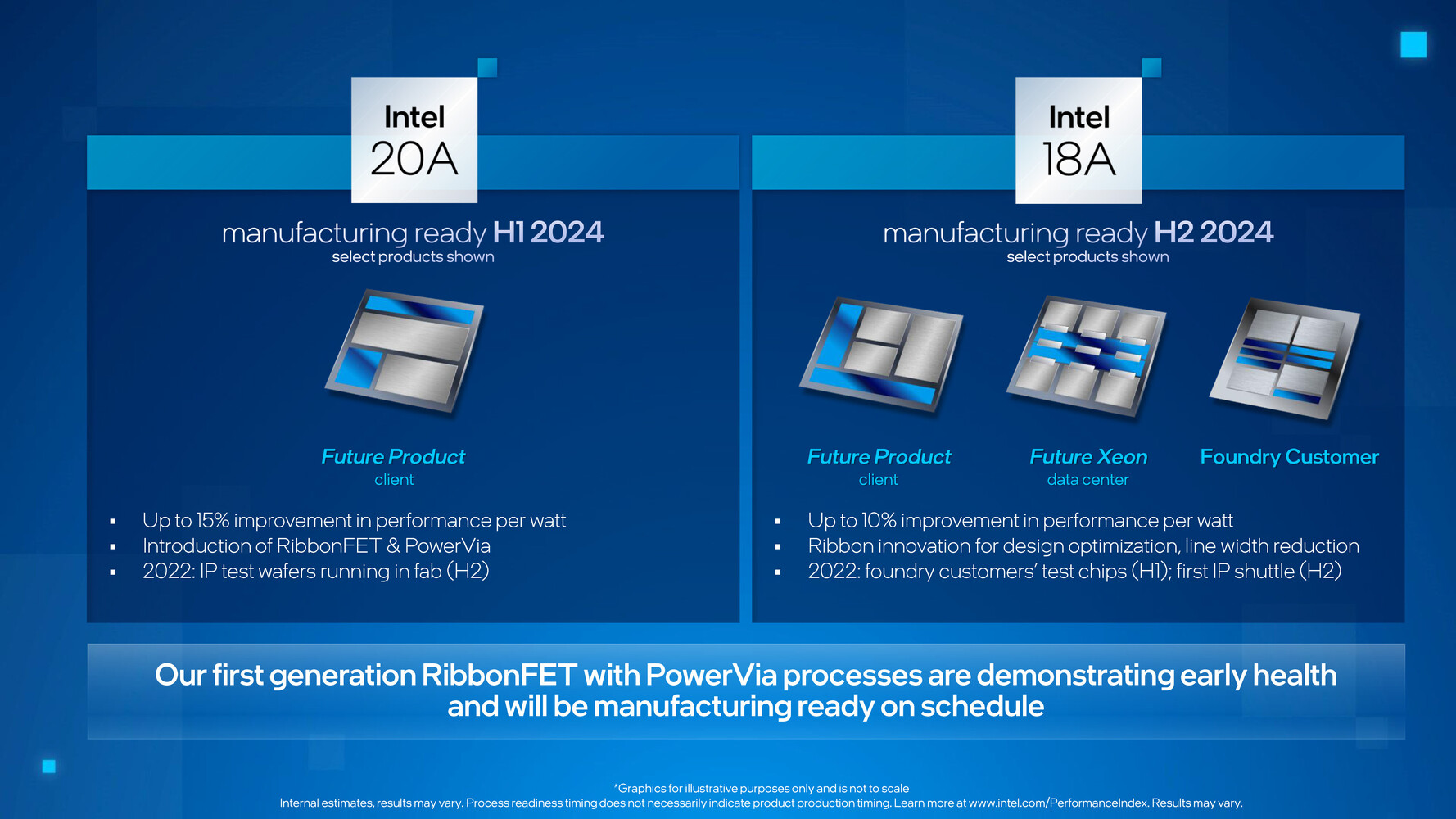
Intel 20A and 18A Foundry Nodes Complete Development Phase, On Track for 2024 Manufacturing

Intel Foundry Services, the in-house semiconductor foundry of Intel, announced that its 2 nm-class Intel 20A and 1.8 nm-class Intel 18A foundry nodes have completed development, and are on course for mass-producing chips on their roadmap dates. Chips are expected to begin mass-production on the Intel 20A node in the first half of 2024, while those on the Intel 18A node are expected to begin in the second half of 2024. The completion of the development phase means that Intel has finalized the specifications and performance/power targets of the nodes, the tools and software required to make the chips, and can now begin ordering them to build the nodes. Intel has been testing these nodes through 2022, and with the specs being finalized, chip-designers can accordingly wrap up development of their products to align with what these nodes have to offer.

Intel 20A (or 20-angstrom, or 2 nm) node introduces gates-all-around (GAA) RibbonFET transistors with PowerVIAs (an interconnect innovation that contributes to transistor densities). The Intel 20A node is claimed to offer a 15% performance/Watt gain over its predecessor, the Intel 3 node (FinFET EUV, 3 nm-class), which by itself offers an 18% performance/Watt gain over Intel 4 (20% perf/Watt gain over the current Intel 7 node), the node that is entering mass-production very soon. The Intel 18A node is a further refinement of Intel 20A, and introduces a design improvement to the RibbonFET that increases transistor density at scale, and a claimed 10% performance/Watt improvement over Intel 20A.

Phison E26 Controller Powering Several Upcoming PCIe Gen 5 NVMe SSDs Detailed

At the 2023 International CES, we caught a hold of Phison, makes or arguably the most popular SSD controllers, which sprung to prominence on being the first to market with PCIe Gen 4 NVMe controllers, and now hopes to repeat it with PCIe Gen 5. We'd been shown a reference-design Phison E26-powered M.2 SSD, along with some hardware specs of the controller itself. The drive itself isn't much to look at—a standard looking M.2-2280 drive with a PCI-Express 5.0 x4 host interface, and the Phison E26 controller with its shiny IHS being prominently located next to a DDR4 memory chip, and two new-generation Micron Technology 3D NAND flash memory chips.

The Phison E26 controller, bearing the long-form model number PS5026-E26, is an NVMe 2.0 spec client-segment SSD controller. It has been built on the TSMC 12 nm FinFET silicon-fabrication node. The controller features an integrated DRAM controller with support for DDR4 and LPDDR4 memory types for use as DRAM cache. Its main flash interface is 8-channel with 32 NAND chip-enable (CE) lines, support for TLC and QLC NAND flash, a dual-CPU architecture, and hardware-acceleration for AES-256, TCG-Opal, and Pyrite. The controller features Phison's 5th generation LPDC ECC and internal RAID engines. For its reference-design 2 TB TLC-based drive, Phison claims sequential transfer rates of up to 13.5 GB/s reads, with up to 12 GB/s writes. The 4K random-access performance is rated at up to 1.5 million IOPS reads, with up to 2 million IOPS writes.

Intel Research Fuels Moore's Law and Paves the Way to a Trillion Transistors by 2030

Today, Intel unveiled research breakthroughs fueling its innovation pipeline for keeping Moore's Law on track to a trillion transistors on a package in the next decade. At IEEE International Electron Devices Meeting (IEDM) 2022, Intel researchers showcased advancements in 3D packaging technology with a new 10x improvement in density; novel materials for 2D transistor scaling beyond RibbonFET, including super-thin material just 3 atoms thick; new possibilities in energy efficiency and memory for higher-performing computing; and advancements for quantum computing.

"Seventy-five years since the invention of the transistor, innovation driving Moore's Law continues to address the world's exponentially increasing demand for computing. At IEDM 2022, Intel is showcasing both the forward-thinking and concrete research advancements needed to break through current and future barriers, deliver to this insatiable demand, and keep Moore's Law alive and well for years to come." -Gary Patton, Intel vice president and general manager of Components Research and Design Enablement

AMD Explains the Economics Behind Chiplets for GPUs

AMD, in its technical presentation for the new Radeon RX 7900 series "Navi 31" GPU, gave us an elaborate explanation on why it had to take the chiplets route for high-end GPUs, devices that are far more complex than CPUs. The company also enlightened us on what sets chiplet-based packages apart from classic multi-chip modules (MCMs). An MCM is a package that consists of multiple independent devices sharing a fiberglass substrate.

An example of an MCM would be a mobile Intel Core processor, in which the CPU die and the PCH die share a substrate. Here, the CPU and the PCH are independent pieces of silicon that can otherwise exist on their own packages (as they do on the desktop platform), but have been paired together on a single substrate to minimize PCB footprint, which is precious on a mobile platform. A chiplet-based device is one where a substrate is made up of multiple dies that cannot otherwise independently exist on their own packages without an impact on inter-die bandwidth or latency. They are essentially what should have been components on a monolithic die, but disintegrated into separate dies built on different semiconductor foundry nodes, with a purely cost-driven motive.

Intel and MediaTek Form Foundry Partnership

Intel and MediaTek today announced a strategic partnership to manufacture chips using Intel Foundry Services' (IFS) advanced process technologies. The agreement is designed to help MediaTek build a more balanced, resilient supply chain through the addition of a new foundry partner with significant capacity in the United States and Europe. MediaTek plans to use Intel process technologies to manufacture multiple chips for a range of smart edge devices. IFS offers a broad manufacturing platform with technologies optimized for high performance, low power and always-on connectivity built on a roadmap that spans production-proven three-dimensional FinFET transistors to next-generation breakthroughs.

"As one of the world's leading fabless chip designers powering more than 2 billion devices a year, MediaTek is a terrific partner for IFS as we enter our next phase of growth," said IFS President Randhir Thakur. "We have the right combination of advanced process technology and geographically diverse capacity to help MediaTek deliver the next billion connected devices across a range of applications."

Samsung Begins Chip Production Using 3nm Process Technology With GAA Architecture

Samsung Electronics, the world leader in semiconductor technology, today announced that it has started initial production of its 3-nanometer (nm) process node applying Gate-All-Around (GAA) transistor architecture. Multi-Bridge-Channel FET (MBCFET), Samsung's GAA technology implemented for the first time ever, defies the performance limitations of FinFET, improving power efficiency by reducing the supply voltage level, while also enhancing performance by increasing drive current capability. Samsung is starting the first application of the nanosheet transistor with semiconductor chips for high performance, low power computing application and plans to expand to mobile processors.

"Samsung has grown rapidly as we continue to demonstrate leadership in applying next-generation technologies to manufacturing, such as foundry industry's first High-K Metal Gate, FinFET, as well as EUV. We seek to continue this leadership with the world's first 3 nm process with the MBCFET," said Dr. Siyoung Choi, President and Head of Foundry Business at Samsung Electronics. "We will continue active innovation in competitive technology development and build processes that help expedite achieving maturity of technology."

Intel Breakthroughs Propel Moore's Law Beyond 2025

In its relentless pursuit of Moore's Law, Intel is unveiling key packaging, transistor and quantum physics breakthroughs fundamental to advancing and accelerating computing well into the next decade. At IEEE International Electron Devices Meeting (IEDM) 2021, Intel outlined its path toward more than 10x interconnect density improvement in packaging with hybrid bonding, 30% to 50% area improvement in transistor scaling, major breakthroughs in new power and memory technologies, and new concepts in physics that may one day revolutionize computing.

"At Intel, the research and innovation necessary for advancing Moore's Law never stops. Our Components Research Group is sharing key research breakthroughs at IEDM 2021 in bringing revolutionary process and packaging technologies to meet the insatiable demand for powerful computing that our industry and society depend on. This is the result of our best scientists' and engineers' tireless work. They continue to be at the forefront of innovations for continuing Moore's Law," said Robert Chau, Intel Senior Fellow and general manager of Components Research.

TrendForce: Annual Foundry Revenue Expected to Reach Historical High Again in 2022 with 13% YoY Increase with Chip Shortage Showing Sign of Easing

While the global electronics supply chain experienced a chip shortage, the corresponding shortage of foundry capacities also led various foundries to raise their quotes, resulting in an over 20% YoY increase in the total annual revenues of the top 10 foundries for both 2020 and 2021, according to TrendForce's latest investigations. The top 10 foundries' annual revenue for 2021 is now expected to surpass US$100 billion. As TSMC leads yet another round of price hikes across the industry, annual foundry revenue for 2022 will likely reach US$117.69 billion, a 13.3% YoY increase.

TrendForce indicates that the combined CAPEX of the top 10 foundries surpassed US$50 billion in 2021, a 43% YoY increase. As new fab constructions and equipment move-ins gradually conclude next year, their combined CAPEX for 2022 is expected to undergo a 15% YoY increase and fall within the US$50-60 billion range. In addition, now that TSMC has officially announced the establishment of a new fab in Japan, total foundry CAPEX will likely increase further next year. TrendForce expects the foundry industry's total 8-inch and 12-inch wafer capacities to increase by 6% YoY and 14% YoY next year, respectively.

Samsung Foundry Announces GAA Ready, 3nm in 2022, 2nm in 2025, Other Speciality Nodes

Samsung Electronics, a world leader in advanced semiconductor technology, today unveiled plans for continuous process technology migration to 3- and 2-nanometer (nm) based on the company's Gate-All-Around (GAA) transistor structure at its 5th annual Samsung Foundry Forum (SFF) 2021. With a theme of "Adding One More Dimension," the multi-day virtual event is expected to draw over 2,000 global customers and partners. At this year's event, Samsung will share its vision to bolster its leadership in the rapidly evolving foundry market by taking each respective part of foundry business to the next level: process technology, manufacturing operations, and foundry services.

"We will increase our overall production capacity and lead the most advanced technologies while taking silicon scaling a step further and continuing technological innovation by application," said Dr. Siyoung Choi, President and Head of Foundry Business at Samsung Electronics. "Amid further digitalization prompted by the COVID-19 pandemic, our customers and partners will discover the limitless potential of silicon implementation for delivering the right technology at the right time."

Foundry Revenue for 2Q21 Reaches Historical High Once Again with 6% QoQ Growth Thanks to Increased ASP and Persistent Demand, Says TrendForce

The panic buying of chips persisted in 2Q21 owing to factors such as post-pandemic demand, industry-wide shift to 5G telecom technology, geopolitical tensions, and chronic chip shortages, according to TrendForce's latest investigations. Chip demand from ODMs/OEMs remained high, as they were unable to meet shipment targets for various end-products due to the shortage of foundry capacities. In addition, wafers inputted in 1Q21 underwent a price hike and were subsequently outputted in 2Q21. Foundry revenue for the quarter reached US$24.407 billion, representing a 6.2% QoQ increase and yet another record high for the eighth consecutive quarter since 3Q19.

Intel Accelerates Packaging and Process Innovations

Intel Corporation today revealed one of the most detailed process and packaging technology roadmaps the company has ever provided, showcasing a series of foundational innovations that will power products through 2025 and beyond. In addition to announcing RibbonFET, its first new transistor architecture in more than a decade, and PowerVia, an industry-first new backside power delivery method, the company highlighted its planned swift adoption of next-generation extreme ultraviolet lithography (EUV), referred to as High Numerical Aperture (High NA) EUV. Intel is positioned to receive the first High NA EUV production tool in the industry.

"Building on Intel's unquestioned leadership in advanced packaging, we are accelerating our innovation roadmap to ensure we are on a clear path to process performance leadership by 2025," Intel CEO Pat Gelsinger said during the global "Intel Accelerated" webcast. "We are leveraging our unparalleled pipeline of innovation to deliver technology advances from the transistor up to the system level. Until the periodic table is exhausted, we will be relentless in our pursuit of Moore's Law and our path to innovate with the magic of silicon."

Intel Debuts 2nd-Gen Horse Ridge Cryogenic Quantum Control Chip

At an Intel Labs virtual event today, Intel unveiled Horse Ridge II, its second-generation cryogenic control chip, marking another milestone in the company's progress toward overcoming scalability, one of quantum computing's biggest hurdles. Building on innovations in the first-generation Horse Ridge controller introduced in 2019, Horse Ridge II supports enhanced capabilities and higher levels of integration for elegant control of the quantum system. New features include the ability to manipulate and read qubit states and control the potential of several gates required to entangle multiple qubits.

"With Horse Ridge II, Intel continues to lead innovation in the field of quantum cryogenic controls, drawing from our deep interdisciplinary expertise bench across the Integrated Circuit design, Labs and Technology Development teams. We believe that increasing the number of qubits without addressing the resulting wiring complexities is akin to owning a sports car, but constantly being stuck in traffic. Horse Ridge II further streamlines quantum circuit controls, and we expect this progress to deliver increased fidelity and decreased power output, bringing us one step closer toward the development of a 'traffic-free' integrated quantum circuit."-Jim Clarke, Intel director of Quantum Hardware, Components Research Group, Intel.

TSMC Completes Its Latest 3 nm Factory, Mass Production in 2022

They say that it is hard to keep up with Moore's Law, however, for the folks over at Taiwan Semiconductor Manufacturing Company (TSMC), that doesn't seem to represent any kind of a problem. Today, to confirm that TSMC is one of the last warriors for the life of Moore's Law, we have information that the company has completed building its manufacturing facility for the next-generation 3 nm semiconductor node. Located in Southern Taiwan Science Park near Tainan, TSMC is expecting to start high-volume manufacturing of the 3 nm node in that Fab in the second half of 2022. As always, one of the first customers expected is Apple.

Estimated to cost an amazing 19.5 billion US Dollars, the Fab is expected to have an output of 55,000 300 mm (12-inch) wafers per month. Given that the regular facilities of TSMC exceed the capacity of over 100K wafers per month, this new facility is expected to increase the capacity over time and possibly reach the 100K level. The new 3 nm node is going to use the FinFET technology and will deliver a 15% performance gain over the previous 5 nm node, with 30% decreased power use and up to 70% density increase. Of course, all of those factors will depend on a specific design.

Samsung's 5 nm Node in Production, First SoCs to Arrive Soon

During its Q3 earnings call, Samsung Electronics has provided everyone with an update on its foundry and node production development. In the past year or so, Samsung's foundry has been a producer of a 7 nm LPP (Low Power Performance) node as its smallest node. That is now changed as Samsung has started the production of the 5 nm LPE (Low Power Early) semiconductor manufacturing node. In the past, we have reported that the company struggled with yields of its 5 nm process, however, that seems to be ironed out and now the node is in full production. To contribute to the statement that the new node is doing well, we also recently reported that Samsung will be the sole manufacturer of Qualcomm Snapdragon 875 5G SoC.

The new 5 nm semiconductor node is a marginal improvement over the past 7 nm node. It features a 10% performance improvement that is taking the same power and chip complexity or a 20% power reduction of the same processor clocks and design. When it comes to density, the company advertises the node with x1.33 times increase in transistor density compared to the previous node. The 5LPE node is manufactured using the Extreme Ultra-Violet (EUV) methodology and its FinFET transistors feature new characteristics like Smart Difusion Break isolation, flexible contact placement, and single-fin devices for low power applications. The node is design-rule compatible with the previous 7 nm LPP node, so the existing IP can be used and manufactured on this new process. That means that this is not a brand new process but rather an enhancement. First products are set to arrive with the next generation of smartphone SoCs, like the aforementioned Qualcomm Snapdragon 875.

TSMC Announces the N12e Enhanced 12nm FF Node for 5G and IoT Edge Devices

TSMC on Monday announced the N12e silicon fabrication node. An enhancement of its 12 nm FinFET node, N12e is designed for value 5G application processors, MODEMs, and IoT edge devices, such as true-wireless earbuds, smartwatch processors, wearables, VR HMDs, entry-level and mainstream SoCs, etc. The node has been derived from the company's 12FFC+_ULL node, and fits into the 12-16 nm class of nodes. It's intended to succeed the company's 22ULL node (in terms of pricing), offering a 76% increase in logic density, 49% increase in clock speed at a given power, 55% improvement in power draw at a given speed, 50% reduction in SRAM leakage current, and low Vdd, with support for logic voltages as low as 0.4 V. That last bit in particular should make the node suitable for tiny, battery-powered devices such as wearables.

Lightmatter Introduces Optical Processor to Speed Compute for Next-Gen AI

Lightmatter, a leader in silicon photonics processors, today announces its artificial intelligence (AI) photonic processor, a general-purpose AI inference accelerator that uses light to compute and transport data. Using light to calculate and communicate within the chip reduces heat—leading to orders of magnitude reduction in energy consumption per chip and dramatic improvements in processor speed. Since 2010, the amount of compute power needed to train a state-of-the-art AI algorithm has grown at five times the rate of Moore's Law scaling—doubling approximately every three and a half months. Lightmatter's processor solves the growing need for computation to support next-generation AI algorithms.

"The Department of Energy estimates that by 2030, computing and communications technology will consume more than 8 percent of the world's power. Transistors, the workhorse of traditional processors, aren't improving; they're simply too hot. Building larger and larger datacenters is a dead end path along the road of computational progress," said Nicholas Harris, PhD, founder and CEO at Lightmatter. "We need a new computing paradigm. Lightmatter's optical processors are dramatically faster and more energy efficient than traditional processors. We're simultaneously enabling the growth of computing and reducing its impact on our planet."

Intel Delivers Advances Across 6 Pillars of Technology, Powering Our Leadership Product Roadmap

At Intel, we truly believe in the potential of technology to enrich lives and change the world. This has been a guiding principle since the company was founded. It started with the PC era, when technology enabled the mass digitization of knowledge and networking, bringing 1 billion people onto the internet. Then came the mobile and cloud era, a disruption that changed the way we live. We now have over 10 billion devices connected to supercomputers in the cloud.

We believe the next era will be the intelligent era. An era where we will experience 100 billion intelligent connected devices. Exascale performance and architecture will make this intelligence available to all, enriching our lives in more ways than we can imagine today. This is a future that inspires and motivates me and my fellow Intel architects every day.

Chinese Fabs Attracted Over 100 TSMC Veteran Engineers Since 2019: Report

A Nikkei investigative report uncovered that two Chinese semiconductor fabrication firms, namely Quanxin Integrated Circuit Manufacturing (QXIC), and Hongxin Semiconductor Manufacturing Co (HSMC), have poached over 100 veteran semiconductor engineers from TSMC since last year. Both firms are recipients of government funding under China's ambitious plan of complete electronics hardware industry independence by 2025. Both firms were floated as recently as 2017, and began hiring specialist engineers and executives with connections across the semiconductor industry, from TSMC. The two began development of a 14 nm-class FinFET node that would support manufacturing of a wide variety of electronics components, including SoCs, ASICs, transceivers, and storage products.

Nikkei estimates that in a span of a year, Taiwan lost more than 3,000 semiconductor engineers to various start-ups in the mainland, including large semiconductor fabs. Sources in TSMC tell the Japanese publication that the company is "very concerned" about the flight of talent toward China, although it didn't believe that there is any immediate danger to the company's output or technological edge. The source advocated a national-level strategy by various Asian governments to retain talent, not through coercion, but by offering better incentives and pay than the Chinese firms flush with public investment.

Intel "Tiger Lake" Leverages 10 nm+ SuperFin and SuperMIM Technologies

Intel's upcoming 11th Generation Core "Tiger Lake" processors introduce the company's first major refinement of its 10 nanometer silicon fabrication node, dubbed 10 nm+. The node introduces two key features that work to improve the power characteristics of the silicon, allowing Intel to yield more performance without raising power/thermals over the previous generation. VideoCardz scored a major scoop on 10 nm+, including the introduction of the new SuperFin transistor, and SuperMIM capacitor.

SuperFin is a redesigned FinFET, a nanoscale transistor, which offers increased gate pitch, yielding higher drive current, improved channel mobility, and an improved source/drain, yielding in lower resistance. The other key component of 10 nm+ is SuperMIM, delivering a 5 times increase in metal-insulator-metal capacitance. Intel is yet to put out energy efficiency gain numbers for the process, but promises a "dramatic increase in frequency" over the previous generation, which lines up with leaks of the Core i7-1185G7 shipping with significantly higher clock speeds.

New AMD Radeon Pro 5000 XT Series GPUs Bring Exceptional Graphics Performance to Updated 27-inch Apple iMac

AMD today announced availability of new AMD Radeon Pro 5000 series GPUs for the updated 27-inch iMac. The new GPUs power a wide variety of graphically intensive applications and workloads, unleashing creativity and productivity for consumer and professional users alike. The new AMD Radeon Pro 5000 series GPUs are built on industry-leading 7 nm process technology and advanced AMD RDNA graphics architecture. They feature up to 40 compute units and up to 16 GB of high-speed GDDR6 memory while delivering up to 7.6 teraflops of single precision (FP32) computational performance.

"AMD Radeon Pro 5000 series GPUs bring new levels of performance and flexibility to the updated 27-inch iMac," said Scott Herkelman, corporate vice president and general manager, Graphics Business Unit at AMD. "The new AMD GPUs offer the optimal combination of compute performance, energy efficiency and outstanding graphics features to power a wide range of applications - from consumer to pro - wherever graphics matter the most."

Intel Accused of Infringing FinFET Patents of the Microelectronics Institute of the Chinese Academy of Sciences

Today we are finding out that Intel has allegedly infringed FinFET patents of Microelectronics Institute of the Chinese Academy of Sciences. On July 28th, the patent review committee has heard an application that accuses Intel of violating a patent 201110240931.5 commonly referred to as FinFET patent. The patent dates back to 2011, and it comes from the Chinese Academy of Sciences, mainly Microelectronics Institute. The Chinese patent holders are asking for as much as 200 million yuan, which roughly translates to 28,664,380 US dollars. Given that this patent infringement is a major one for Intel, it is sure that a company will be pursued extensively in court. All of the Intel's semiconductors use FinFET technology, and if this is true, the violation is rather big. For more in detail reading, please refer to the source which goes through the history of Intel and Microelectronics Institute patent violation filing.
Intel 3rd generation FInFETs

GLOBALFOUNDRIES Announces 12LP+ Enhanced 12nm Silicon Fabrication Node

GLOBALFOUNDRIES (GF), the world's leading specialty foundry, today announced its most advanced FinFET solution, 12LP+, has completed technology qualification and is ready for production. GF's differentiated 12LP+ solution is optimized for artificial intelligence (AI) training and inference applications. Built on a proven platform with a robust production ecosystem, 12LP+ offers chip designers an efficient development experience and a fast time-to-market.

Contributing to its best-in-class combination of performance, power and area, 12LP+ introduces new features including an updated standard cell library, an interposer for 2.5D packaging, and a low-power 0.5 V Vmin SRAM bitcell that supports the low latency and power-efficient shuttling of data between the AI processors and memory. The result is a semiconductor solution engineered to meet the specific needs of the fast-growing AI market.

Intel Plans to Volume Manufacture Nanowire/Nanoribbon Transistors in Five Years

Semiconductor manufacturing is a hard business. There is a constant need for manufacturers to compete with each other and if they don't, they get left behind. Intel, as one of the biggest semiconductor makers in the world, is always trying to invent new technologies spending massive R&D funds on semiconductors. New technologies such as nanowire/nanoribbon transistors, which are supposed to enable transistor sizes unimaginable now, are on its way to make it in the hand of consumers. During the international VLSI conference, Intel's CTO Mike Mayberry held a presentation about how Intel plans to address the demand for more compute by showing off new technologies.

With a presentation titled "The Future of Compute", Mr. Mayberry made some exciting claims and predictions. So far, we have been used to FinFET transistors since the 22 nm node from Intel. However, as nodes get smaller the gate of the transistor is not enough to keep it from switching randomly. So to avoid that problem Intel, along with other semiconductor manufacturers like Samsung, created a solution called Gate-All-Around FET (GAAFET). This technology takes a transistor fin and wraps in around all sides (see picture below), so the gate has better switching control, preventing random switching and errors. As a fin, nanowire or nanosheet (wider option from nanowire) can be used and they can be stacked. These allow for additional control of tailoring whatever a node will be used for high performance or low power. Intel predicts that they will start high volume manufacturing of silicon based on this technology in five years. This is setting an important milestone for Intel as well as other industry players, as now everyone will rush to deliver it first. It is now a waiting game to see who will actually come out with it first.
Intel Nanowire/Nanoribbon Samsung GAAFET

DigiTimes: TSMC Kicking Off Development of 2nm Process Node

A report via DigiTimes places TSMC as having announced to its investors that exploratory studies and R&D for the development of the 2 nm process node have commenced. As today's leading semiconductor fabrication company, TSMC doesn't seem to be one resting on its laurels. Their 7 nm process and derivatives have already achieved a 30% weight on the company's semiconductor orders, and their 5 nm node (which will include EUV litography) is set to hit HVM (High Volume Manufacturing) in Q2 of this year. Apart from that, not much more is known on 2 nm.

After 5 nm, which is expected to boats of an 84-87% transistor density gain over the current 7nm node, the plans are to go 3nm, with TSMC expecting that node to hit mass production come 2022. Interestingly, TSMC is planning to still use FinFET technology for its 3 nm manufacturing node, though in a new GAAFET (gate-all-around field-effect transistor) technology. TSMC's plans to deploy FinFET in under 5nm manufacturing is something that many industry analysts and specialist thought extremely difficult to achieve, with expectations for these sub-5nm nodes to require more exotic materials and transistor designs than TSMC's apparent plans
Return to Keyword Browsing
Jul 4th, 2025 03:28 CDT change timezone

New Forum Posts

Popular Reviews

TPU on YouTube

Controversial News Posts