Apr 16th, 2025 09:19 EDT
change timezone
Latest GPU Drivers
New Forum Posts
- Last game you purchased? (772)
- Help me identify Chip of this DDR4 RAM (20)
- 5070ti overclock...what are your settings? (5)
- Windows 11 fresh install to do list (23)
- How to relubricate a fan and/or service a troublesome/noisy fan. (229)
- GPU Memory Temprature is always high (16)
- Help For XFX RX 590 GME Chinese - Vbios (4)
- PCGH: "hidden site" to see total money spend on steam (3)
- Share your AIDA 64 cache and memory benchmark here (3053)
- NVFlash for RTX 50 Series (Blackwell) (0)
Popular Reviews
- G.SKILL Trident Z5 NEO RGB DDR5-6000 32 GB CL26 Review - AMD EXPO
- ASUS GeForce RTX 5080 TUF OC Review
- DAREU A950 Wing Review
- The Last Of Us Part 2 Performance Benchmark Review - 30 GPUs Compared
- Sapphire Radeon RX 9070 XT Pulse Review
- Sapphire Radeon RX 9070 XT Nitro+ Review - Beating NVIDIA
- Upcoming Hardware Launches 2025 (Updated Apr 2025)
- Thermaltake TR100 Review
- Zotac GeForce RTX 5070 Ti Amp Extreme Review
- TerraMaster F8 SSD Plus Review - Compact and quiet
Controversial News Posts
- NVIDIA GeForce RTX 5060 Ti 16 GB SKU Likely Launching at $499, According to Supply Chain Leak (182)
- NVIDIA Sends MSRP Numbers to Partners: GeForce RTX 5060 Ti 8 GB at $379, RTX 5060 Ti 16 GB at $429 (124)
- Nintendo Confirms That Switch 2 Joy-Cons Will Not Utilize Hall Effect Stick Technology (105)
- Over 200,000 Sold Radeon RX 9070 and RX 9070 XT GPUs? AMD Says No Number was Given (100)
- Nintendo Switch 2 Launches June 5 at $449.99 with New Hardware and Games (99)
- Sony Increases the PS5 Pricing in EMEA and ANZ by Around 25 Percent (85)
- NVIDIA PhysX and Flow Made Fully Open-Source (77)
- NVIDIA Pushes GeForce RTX 5060 Ti Launch to Mid-April, RTX 5060 to May (77)
News Posts matching #TSMC
Return to Keyword Browsing
AMD Achieves First TSMC N2 Product Silicon Milestone
AMD today announced its next-generation AMD EPYC processor, codenamed "Venice," is the first HPC product in the industry to be taped out and brought up on the TSMC advanced 2 nm (N2) process technology. This highlights the strength of AMD and TSMC semiconductor manufacturing partnership to co-optimize new design architectures with leading-edge process technology. It also marks a major step forward in the execution of the AMD data center CPU roadmap, with "Venice" on track to launch next year. AMD also announced the successful bring up and validation of its 5th Gen AMD EPYC CPU products at TSMC's new fabrication facility in Arizona, underscoring its commitment to U.S. manufacturing.
"TSMC has been a key partner for many years and our deep collaboration with their R&D and manufacturing teams has enabled AMD to consistently deliver leadership products that push the limits of high-performance computing," said Dr. Lisa Su, chair and CEO, AMD. "Being a lead HPC customer for TSMC's N2 process and for TSMC Arizona Fab 21 are great examples of how we are working closely together to drive innovation and deliver the advanced technologies that will power the future of computing."
"TSMC has been a key partner for many years and our deep collaboration with their R&D and manufacturing teams has enabled AMD to consistently deliver leadership products that push the limits of high-performance computing," said Dr. Lisa Su, chair and CEO, AMD. "Being a lead HPC customer for TSMC's N2 process and for TSMC Arizona Fab 21 are great examples of how we are working closely together to drive innovation and deliver the advanced technologies that will power the future of computing."


Intel's 18A Node Outperforms TSMC N2 and Samsung SF2 in 2 nm Performance Class
Intel's 18A node isn't all about yields and density (which are still very important factors) but also performance. According to Taiwanese media 3C News, citing TechInsights research and calculations, the new leader of node performance is Intel 18A. On a custom scale used by TechInsights, Intel 18A gets a 2.53 score, while the performance score of TSMC N2 is 2.27, and the performance score of Samsung SF2 is 2.19. This is all among two nm-class nodes, where Intel leads the category. Being the first node with a Backside Power Delivery Network (BSPDN), it will appear in the Panther Lake CPUs in late 2025 for testing and early 2026 for shipments. This new power architecture boosts layout efficiency and component utilization by 5-10%, lowers interconnect resistance, and enhances ISO power performance by up to 4%, thanks to a significant drop in intrinsic resistance versus traditional front‑end power routing. Relative to its predecessor, Intel 3, the 18A process delivers a 15% improvement in performance per watt and packs 30% more transistors into the same area.
Featuring RibbonFET design, it has entered risk production. According to Intel, "This final stage is about stress-testing volume manufacturing before scaling up to high volume in the second half of 2025." When it comes to other aspects like SRAM density, high‑performance SRAM cells shrank from 0.03 µm² in Intel 3 to 0.023 µm² in Intel 18A, while high‑density cells contracted to 0.021 µm², reflecting scaling factors of 0.77 and 0.88 respectively and defying previous assumptions that SRAM scaling had plateaued. Intel's innovative "around‑the‑array" PowerVia approach addresses voltage drops and interference by routing power vias to I/O, control, and decoder circuits, freeing up the bit‑cell area from frontal power supplies. The result is a 38.1 Mbit/mm² macro bit density, positioning Intel to rival TSMC's N2. All this, combined with BSPDN, is shaping up a powerful node. We can't wait to get our hands on some 18A silicon in the future and run it through our labs for testing.
Featuring RibbonFET design, it has entered risk production. According to Intel, "This final stage is about stress-testing volume manufacturing before scaling up to high volume in the second half of 2025." When it comes to other aspects like SRAM density, high‑performance SRAM cells shrank from 0.03 µm² in Intel 3 to 0.023 µm² in Intel 18A, while high‑density cells contracted to 0.021 µm², reflecting scaling factors of 0.77 and 0.88 respectively and defying previous assumptions that SRAM scaling had plateaued. Intel's innovative "around‑the‑array" PowerVia approach addresses voltage drops and interference by routing power vias to I/O, control, and decoder circuits, freeing up the bit‑cell area from frontal power supplies. The result is a 38.1 Mbit/mm² macro bit density, positioning Intel to rival TSMC's N2. All this, combined with BSPDN, is shaping up a powerful node. We can't wait to get our hands on some 18A silicon in the future and run it through our labs for testing.


NVIDIA & Partners to Produce American-made AI Supercomputers in US for First Time
NVIDIA is working with its manufacturing partners to design and build factories that, for the first time, will produce NVIDIA AI supercomputers entirely in the U.S. Together with leading manufacturing partners, the company has commissioned more than a million square feet of manufacturing space to build and test NVIDIA Blackwell chips in Arizona and AI supercomputers in Texas. NVIDIA Blackwell chips have started production at TSMC's chip plants in Phoenix, Arizona. NVIDIA is building supercomputer manufacturing plants in Texas, with Foxconn in Houston and with Wistron in Dallas. Mass production at both plants is expected to ramp up in the next 12-15 months. The AI chip and supercomputer supply chain is complex and demands the most advanced manufacturing, packaging, assembly and test technologies. NVIDIA is partnering with Amkor and SPIL for packaging and testing operations in Arizona.
Within the next four years, NVIDIA plans to produce up to half a trillion dollars of AI infrastructure in the United States through partnerships with TSMC, Foxconn, Wistron, Amkor and SPIL. These world-leading companies are deepening their partnership with NVIDIA, growing their businesses while expanding their global footprint and hardening supply chain resilience. NVIDIA AI supercomputers are the engines of a new type of data center created for the sole purpose of processing artificial intelligence—AI factories that are the infrastructure powering a new AI industry. Tens of "gigawatt AI factories" are expected to be built in the coming years. Manufacturing NVIDIA AI chips and supercomputers for American AI factories is expected to create hundreds of thousands of jobs and drive trillions of dollars in economic security over the coming decades.


Within the next four years, NVIDIA plans to produce up to half a trillion dollars of AI infrastructure in the United States through partnerships with TSMC, Foxconn, Wistron, Amkor and SPIL. These world-leading companies are deepening their partnership with NVIDIA, growing their businesses while expanding their global footprint and hardening supply chain resilience. NVIDIA AI supercomputers are the engines of a new type of data center created for the sole purpose of processing artificial intelligence—AI factories that are the infrastructure powering a new AI industry. Tens of "gigawatt AI factories" are expected to be built in the coming years. Manufacturing NVIDIA AI chips and supercomputers for American AI factories is expected to create hundreds of thousands of jobs and drive trillions of dollars in economic security over the coming decades.


Trump Exempts Electronics and GPUs from China Tariffs to Ease Tech Costs
President Trump announced late Friday that a range of electronics imported from China will not be hit by his new reciprocal tariffs, according to a US Customs and Border Protection notice. The exemption, which applies to items arriving in the United States or leaving bonded warehouses on or after April 5, covers smartphones, computer monitors, semiconductors, various electronic parts, and, importantly, high-performance GPUs. Tech companies were bracing for big cost increases. Apple, for example, assembles about 90 percent of its iPhones in China and holds roughly six weeks of inventory in US warehouses. Without this exemption, consumers would likely have seen higher prices once that stock ran out. Framework, the modular laptop maker, has already paused US sales of some Laptop 13 models and discounted others by up to 12 percent after a new 10 percent tariff on Taiwanese parts squeezed their margins.
The GPU market got another break thanks to a clever workaround in the United States-Mexico-Canada Agreement. A research firm SemiAnalysis pointed out that graphics cards made in Taiwan can still enter the US tariff-free if they undergo final assembly in Mexico or Canada. That loophole applies to digital processing units and related circuit boards, which means companies relying on NVIDIA's top-tier accelerators for AI won't see an immediate price jump. White House Press Secretary Karoline Leavitt said these steps are part of a two-pronged plan: offering short-term relief to keep consumer prices down while at the same time pushing major tech firms like Apple, TSMC, and NVIDIA to invest billions in US manufacturing. However, many experts warn that high-precision components are still largely made in Asia, so building up domestic production capacity could take months or even years and may remain more expensive in the meantime.
Update: President Donald Trump posted on Truth Social the following: "There was no Tariff "exception" announced on Friday. These products are subject to the existing 20% Fentanyl Tariffs, and they are just moving to a different Tariff "bucket."We are taking a look at Semiconductors and the WHOLE ELECTRONICS SUPPLY CHAIN in the upcoming National Security Tariff Investigations."


TSMC Faces $1 Billion Fine from US Government Over Shipments to Huawei
TSMC is confronting a potential $1 billion-plus penalty from the US Commerce Department after inadvertently fabricating compute chiplets later integrated into Huawei's Ascend 910 AI processor. The fine, potentially reaching twice the value of unauthorized shipments, reflects the scale of components that circumvented export controls limiting Chinese access to advanced semiconductor technology. The regulatory breach originated in late 2023 when TSMC processed orders from Sophgo, a design partner of crypto-mining firm Bitmain. These chiplets, which are manufactured on advanced process nodes and contain tens of billions of transistors, were identified in TechInsights teardown analysis of Huawei Ascend 910 AI accelerator, revealing a supply chain vulnerability where TSMC lacked visibility into the components' end-use.
Upon discovery of the diversion, TSMC immediately halted Sophgo shipments and engaged in discussions with Commerce Department officials. By January, Sophgo had been added to the Entity List, limiting its access to US semiconductor technology. A Center for Strategic and International Studies report revealed that Huawei obtained approximately two million Ascend 910B logic dies through shell companies that misled TSMC. Huawei's preference for TSMC-made dies was due to manufacturing challenges in domestic chip production. This incident has forced TSMC to strengthen its customer vetting protocols, including terminating its relationship with Singapore-based PowerAIR following internal compliance reviews. The enforcement process typically begins with a proposed charging letter detailing violations and penalty calculations, followed by a 30-day response period. As Washington tightens restrictions on AI processor exports to Chinese entities, semiconductor manufacturers are under increased pressure to implement rigorous controls throughout multinational supply chains.
Upon discovery of the diversion, TSMC immediately halted Sophgo shipments and engaged in discussions with Commerce Department officials. By January, Sophgo had been added to the Entity List, limiting its access to US semiconductor technology. A Center for Strategic and International Studies report revealed that Huawei obtained approximately two million Ascend 910B logic dies through shell companies that misled TSMC. Huawei's preference for TSMC-made dies was due to manufacturing challenges in domestic chip production. This incident has forced TSMC to strengthen its customer vetting protocols, including terminating its relationship with Singapore-based PowerAIR following internal compliance reviews. The enforcement process typically begins with a proposed charging letter detailing violations and penalty calculations, followed by a 30-day response period. As Washington tightens restrictions on AI processor exports to Chinese entities, semiconductor manufacturers are under increased pressure to implement rigorous controls throughout multinational supply chains.

Xiaomi's Proprietary Flagship Mobile SoC Reportedly Downgraded to TSMC "N4P"
According to reports from last year, Xiaomi was expected to unveil an oft-rumored proprietary mobile chipset design at some point in 2025. By October 2024, the Chinese technology giant allegedly reached the tape-out phase of its first 3 nm SoC—at the time, insiders posited that Xiaomi was seeking a manufacturing partner. Months earlier, a prototype design was linked to TSMC's 4 nm "N4P" node process—this rumor raised many smartphone watchdog eyebrows. Unlike many other Chinese firms, Xiaomi was reportedly allowed to select a fairly advanced manufacturing process at Taiwan's premier foundry service. In a past weekend news article, Wccftech outlined interesting circumstances: "(US) export controls have yet to affect Xiaomi, which is supposedly on track to launch its first in-house chipset later this year. However, while we reported last year that the company was scheduled to unveil its custom 3 nm SoC in 2025, we were disappointed to learn just the specifications of this version that will utilize TSMC's 'N4P' process. According to more details, this silicon will not sport any homegrown cores like Qualcomm has adopted for the Snapdragon 8 Elite."
Late last week, Jukanlosreve highlighted another leaker's prediction—regarding the technological foundations of Xiaomi's mystery flagship mobile processor. Fixed Focus Digital's Weibo post mentioned the "N4P" node, as well the utilization of current generation Arm Cortex-X925, Cortex-A725 and Cortex-A520 units. A speculated Imagination Technologies "IMG DXT 72-2304" integrated graphics solution is touted to outperform Qualcomm's Adreno 740 iGPU; as featured in their Snapdragon 8 Gen 2 (2022) SoC. As highlighted by Wccftech's report, one of the publication's associates has deemed Fixed Focus Digital to be an unreliable source of inside track info. In response to Jukanlosreve's tweeted question, Mochamad Farido Fanani opined: "that's right, how does Xiaomi use N4P in its new chipset? But this guy always guesses blindly." Older leaks—based on "N4P" rumors—projected performance levels roughly on par with Qualcomm's first generation Snapdragon 8 chip. This model was introduced at the tail end of 2021.


Late last week, Jukanlosreve highlighted another leaker's prediction—regarding the technological foundations of Xiaomi's mystery flagship mobile processor. Fixed Focus Digital's Weibo post mentioned the "N4P" node, as well the utilization of current generation Arm Cortex-X925, Cortex-A725 and Cortex-A520 units. A speculated Imagination Technologies "IMG DXT 72-2304" integrated graphics solution is touted to outperform Qualcomm's Adreno 740 iGPU; as featured in their Snapdragon 8 Gen 2 (2022) SoC. As highlighted by Wccftech's report, one of the publication's associates has deemed Fixed Focus Digital to be an unreliable source of inside track info. In response to Jukanlosreve's tweeted question, Mochamad Farido Fanani opined: "that's right, how does Xiaomi use N4P in its new chipset? But this guy always guesses blindly." Older leaks—based on "N4P" rumors—projected performance levels roughly on par with Qualcomm's first generation Snapdragon 8 chip. This model was introduced at the tail end of 2021.


Intel and TSMC in Foundry Joint Venture Talks
Intel and TSMC are reportedly locked in talks to form a semiconductor foundry joint-venture (JV). This sensational piece of news comes from Reuters, which says that the two companies have reached a preliminary agreement to form the JV. Apparently, the move saves TSMC from building any hard infrastructure on U.S. soil, and instead use Intel's semiconductor foundry facilities. This would hence bring TSMC's semiconductor manufacturing IP and workforce to the U.S., however it remains to be seen if the very latest foundry technology would be handed over to the JV. TSMC would hold a 20% stake in the venture, and Intel the rest. Investors of Intel and TSMC reacted very differently to the news, with the TSMC stock falling 6% and Intel gaining 5%. Reuters also reports that it was the Trump Administration that negotiated this joint-venture between TSMC and Intel in a bid to "revitalize Intel."

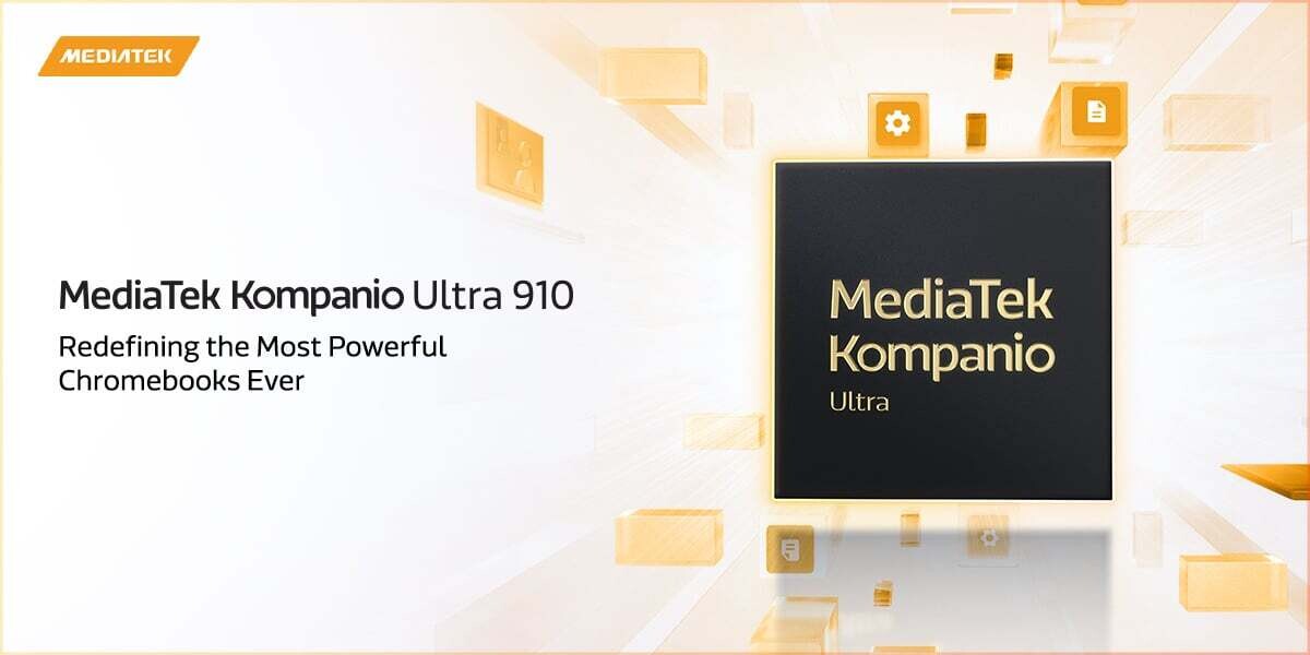
MediaTek Introduces Kompanio Ultra SoC, Touted to Redefine AI Performance for Chromebook Plus
MediaTek has introduced the Kompanio Ultra, the latest milestone in AI-powered, high-performance Chromebooks. Leveraging MediaTek's proven expertise in flagship innovation, this powerful new platform brings fantastic on-device AI capabilities, superior computing performance, and industry-leading power efficiency to the newest Chromebook Plus devices. "The Kompanio Ultra underscores our commitment to delivering groundbreaking computing performance and efficiency that MediaTek has shown as a leader in the mobile compute space for many years," said Adam King, Vice President & General Manager of Computing and Multimedia Business at MediaTek. "We worked closely with Google to ensure the newest Chromebook Plus devices enjoy next-generation on-device AI capabilities, superior performance per watt, and immersive multimedia."
The Kompanio Ultra is MediaTek's most powerful Chromebook processor to date, integrating 50 TOPS of AI processing power to enable on-device generative AI experiences. With MediaTek's 8th-generation NPU, users can expect real-time task automation, personalized computing, and seamless AI-enhanced workflows—with local processing for enhanced speed, security, efficiency, and support for AI workloads without an internet connection. Built on the cutting-edge (TSMC) 3 nm process, the Kompanio Ultra features an all-big-core CPU architecture with an Arm Cortex-X925 processor clocked at up to 3.62 GHz, delivering industry-leading single and multithreaded performance. Whether handling intensive applications like video editing, content creation, or high-resolution gaming, this processor ensures smooth, lag-free performance with unmatched multitasking capabilities.


The Kompanio Ultra is MediaTek's most powerful Chromebook processor to date, integrating 50 TOPS of AI processing power to enable on-device generative AI experiences. With MediaTek's 8th-generation NPU, users can expect real-time task automation, personalized computing, and seamless AI-enhanced workflows—with local processing for enhanced speed, security, efficiency, and support for AI workloads without an internet connection. Built on the cutting-edge (TSMC) 3 nm process, the Kompanio Ultra features an all-big-core CPU architecture with an Arm Cortex-X925 processor clocked at up to 3.62 GHz, delivering industry-leading single and multithreaded performance. Whether handling intensive applications like video editing, content creation, or high-resolution gaming, this processor ensures smooth, lag-free performance with unmatched multitasking capabilities.


GUC Announces Tape-Out of the World's First HBM4 IP on TSMC N3P
Global Unichip Corp. (GUC), the Advanced ASIC Leader, announced today that it has successfully taped-out the world's first HBM4 controller and PHY IP. This test chip was implemented using TSMC's cutting-edge N3P process technology and CoWoS -R advanced packaging technology.
The HBM4 IP supports data rates of up to 12 Gbps under all operating conditions. By leveraging a proprietary interposer layout, GUC has optimized signal integrity (SI) and power integrity (PI) to achieve these high speeds for all types of CoWoS technology. Comparing with HBM3, GUC's HBM4 PHY delivers 2.5x bandwidth while improving 1.5x power efficiency and 2x area efficiency. In line with previous GUC HBM, GLink, and UCIe IPs, this HBM4 IP integrates proteanTecs' interconnect monitoring solution to provide high visibility for testing and characterizing the PHY while improving in-field performance and reliability for end products.
The HBM4 IP supports data rates of up to 12 Gbps under all operating conditions. By leveraging a proprietary interposer layout, GUC has optimized signal integrity (SI) and power integrity (PI) to achieve these high speeds for all types of CoWoS technology. Comparing with HBM3, GUC's HBM4 PHY delivers 2.5x bandwidth while improving 1.5x power efficiency and 2x area efficiency. In line with previous GUC HBM, GLink, and UCIe IPs, this HBM4 IP integrates proteanTecs' interconnect monitoring solution to provide high visibility for testing and characterizing the PHY while improving in-field performance and reliability for end products.

US Exempts Semiconductors From Taiwan Tariffs, But Chip-Making Equipment Remains on the List
Yesterday, United States President Donald Trump announced a set of tariffs imposed on US trading partners, imposing a series of 10%+ tariffs on partners, calling it a "Liberation Day." Today, we are calculating how much these tariffs will impact consumers and what is most important at TechPowerUp: semiconductors powering our GPUs and CPUs. According to one of the top investment banks, Goldman Sachs, semiconductors are exempt from the reciprocal tariffs that Trump has imposed on Taiwan. However, the semiconductor manufacturing equipment used by makers like TSMC is not exempt and is expected to be hit with the 32% tariffs. This is only half of what Taiwan imposes on imports of US-made goods. For TSMC, the number one maker of GPUs and CPUs, tariffs can be tricky to navigate. While its existing manufacturing facilities use equipment sourced from Dutch ASML and a few US companies like Lam Research and KLA Corporation, it shouldn't be a problem to ship new silicon to the US.
However, if TSMC wants to expand its manufacturing facilities in any country that is not the US, it will have to deal with 32% tariffs on US-sourced silicon manufacturing equipment. For EU-based ASML, things are looking a little different. If over 20% of the equipment is made up of US content, a tariff exemption might apply, potentially reducing import costs. If more than one-fifth of a product's components or value originates from US sources, the equipment may be eligible for tariff relief. ASML's machines include some US components, so determining whether these machines meet the 20% threshold is crucial. If they do, the tariff exemption could help lower costs associated with importing these advanced machines, reaching up to $380 million. For non-US-injected goods, EU entities are subject to 20% tariffs.
However, if TSMC wants to expand its manufacturing facilities in any country that is not the US, it will have to deal with 32% tariffs on US-sourced silicon manufacturing equipment. For EU-based ASML, things are looking a little different. If over 20% of the equipment is made up of US content, a tariff exemption might apply, potentially reducing import costs. If more than one-fifth of a product's components or value originates from US sources, the equipment may be eligible for tariff relief. ASML's machines include some US components, so determining whether these machines meet the 20% threshold is crucial. If they do, the tariff exemption could help lower costs associated with importing these advanced machines, reaching up to $380 million. For non-US-injected goods, EU entities are subject to 20% tariffs.


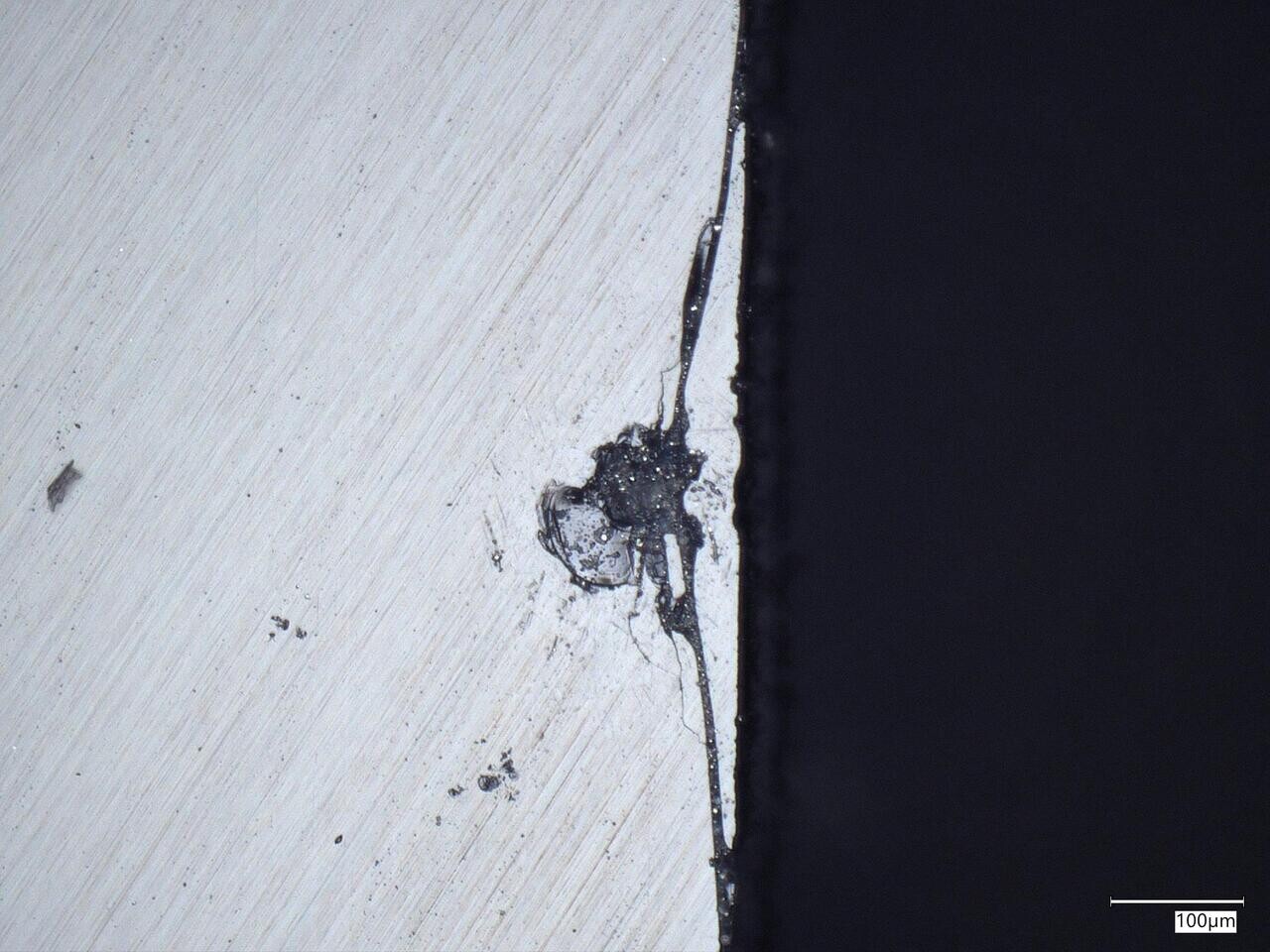
GPU Die Defects Found in PowerColor RX 9070 XT Graphics Card
Surface defects on the GPU die of a PowerColor Radeon RX 9070 XT Hellhound have been linked to excessive thermal hotspots, according to analysis following Igor's Lab's investigation. Microscopic examination revealed 1,934 pits across the silicon die surface despite proper thermal interface material application. The defects affect over one percent of the chip's surface area, with the largest measuring 12.59 µm in depth and 212.36 µm in diameter—significantly exceeding industry tolerances. These imperfections impede heat transfer, causing localized temperatures to reach 113°C, exceeding the 110°C threshold for RDNA GPUs and triggering thermal throttling. The defects appear to stem from flaws in the backgrinding process that thins silicon wafers for packaging. Improper process control creates surface irregularities that compromise thermal conductivity and structural integrity.
The discovery raises questions about the effectiveness of automated optical inspection systems in detecting subtle surface abnormalities. TSMC, the maker of these chips, uses optical recognition tools to see if any defects occurred. AMD stated: "We are aware of the reported issue and believe this to be an isolated incident. We are working with our partners and internal teams to understand the issue." The company maintains this is an isolated case, though the findings suggest potential gaps in quality control protocols. Users experiencing thermal issues with affected RX 9070 XT units should initiate the RMA process for replacement while AMD and PowerColor investigate whether these defects exist beyond the identified sample. We hope no further issues are present, and so far, PowerColor hasn't received any customer complaints. We are on the lookout for further situation development. We reviewed PowerColor's Radeon RX 9070 Hellhound, and found no issues on our unit, so this indeed remains an isolated case so far.


The discovery raises questions about the effectiveness of automated optical inspection systems in detecting subtle surface abnormalities. TSMC, the maker of these chips, uses optical recognition tools to see if any defects occurred. AMD stated: "We are aware of the reported issue and believe this to be an isolated incident. We are working with our partners and internal teams to understand the issue." The company maintains this is an isolated case, though the findings suggest potential gaps in quality control protocols. Users experiencing thermal issues with affected RX 9070 XT units should initiate the RMA process for replacement while AMD and PowerColor investigate whether these defects exist beyond the identified sample. We hope no further issues are present, and so far, PowerColor hasn't received any customer complaints. We are on the lookout for further situation development. We reviewed PowerColor's Radeon RX 9070 Hellhound, and found no issues on our unit, so this indeed remains an isolated case so far.


Apple Reportedly Eyeing Late 2025 Launch of M5 MacBook Pro Series, M5 MacBook Air Tipped for 2026
Mark Gurman—Bloomberg's resident soothsayer of Apple inside track info—has disclosed predictive outlooks for next-generation M5 chip-based MacBooks. Early last month, we experienced the launch of the Northern Californian company's M4 MacBook Air series—starting at $999; also available in a refreshing metallic blue finish. The latest iteration of Apple's signature "extra slim" notebook family arrived with decent performance figures. As per usual, press and community attention has turned to a potential successor. Gurman's (March 30) Power On newsletter posited that engineers are already working on M5-powered super slim sequels—he believes that these offerings will arrive early next year, potentially reusing the current generation's 15-inch and 13-inch fanless chassis designs.
In a mid-February predictive report, Gurman theorized that Apple was planning a major overhaul of the MacBook Pro design. A radical reimagining of the long-running notebook series—that reportedly utilizes M6 chipsets and OLED panels—is a distant prospect; perhaps later on in 2026. The Cupertino-headquartered megacorp is expected to stick with its traditional release cadence, so 2025's "M5" refresh of MacBook Pro models could trickle out by October. Insiders believe that Apple will reuse existing MacBook Pro shells—the last major redesign occurred back in 2021. According to early February reportage, mass production of the much-rumored M5 chip started at some point earlier in the year. Industry moles posit that a 3 nm (N3P) node process was on the order books, chez TSMC foundries.


In a mid-February predictive report, Gurman theorized that Apple was planning a major overhaul of the MacBook Pro design. A radical reimagining of the long-running notebook series—that reportedly utilizes M6 chipsets and OLED panels—is a distant prospect; perhaps later on in 2026. The Cupertino-headquartered megacorp is expected to stick with its traditional release cadence, so 2025's "M5" refresh of MacBook Pro models could trickle out by October. Insiders believe that Apple will reuse existing MacBook Pro shells—the last major redesign occurred back in 2021. According to early February reportage, mass production of the much-rumored M5 chip started at some point earlier in the year. Industry moles posit that a 3 nm (N3P) node process was on the order books, chez TSMC foundries.


TSMC Reportedly Preparing New Equipment for 1.4 nm Trial Run at "P2" Baoshan Plant
Industry insiders posit that TSMC's two flagship fabrication facilities are running ahead of schedule with the development of an advanced 2 nm (N2) process node. A cross-facility mass production phase is tipped to begin later this year, which leaves room for next-level experiments. Taiwan's Economic Daily News has heard supply chain whispers about the Baoshan "P2" plant making internal preparations for a truly cutting edge 1.4 nm-class product. According to the report, unnamed sources have claimed that: "TSMC has made a major breakthrough in the advancement of its 1.4 nm process. (The company) has recently notified suppliers to prepare the necessary equipment for 1.4 nm, and plans to install a trial production 'mini-line' at P2 (Baoshan Fab 20)."
Their Hsinchu-adjacent "Fab 20" site is touted as a leading player in the prototyping of this new technology. Industry moles reckon that "1.4 nm expertise" will eventually trickle over to nearby "P3 and P4 plants" for full production phases. Allegedly, these factories were originally going to be involved in the manufacturing of 2 nm (N2) wafers. Additionally, TSMC's "Fab 25" campus could potentially play host to trial 1.4 nm activities—the Economic Daily News article proposes that four plants based in the Central Taiwan Science Park are pitching in with collaborative work. As interpreted by TrendForce, "P1" could begin "risk trial production" by 2027, followed by full-scale output within the following year.


Their Hsinchu-adjacent "Fab 20" site is touted as a leading player in the prototyping of this new technology. Industry moles reckon that "1.4 nm expertise" will eventually trickle over to nearby "P3 and P4 plants" for full production phases. Allegedly, these factories were originally going to be involved in the manufacturing of 2 nm (N2) wafers. Additionally, TSMC's "Fab 25" campus could potentially play host to trial 1.4 nm activities—the Economic Daily News article proposes that four plants based in the Central Taiwan Science Park are pitching in with collaborative work. As interpreted by TrendForce, "P1" could begin "risk trial production" by 2027, followed by full-scale output within the following year.


Report Suggests TSMC's Successful Completion of 2 nm Trial Phase, Cross-facility Mass Production Expected by End of Year
Going back to the start of this year, TSMC's trial run of a cutting-edge 2 nm (N2) node process was reportedly progressing beyond initial expectations. According to industry moles, two flagship fabrication facilities are "optimistically" tipped to pump out 80,000 units per month (by the end of 2025). This cross-facility total figure was linked to TSMC's Baoshan—located near the Northern Taiwanese city of Hsinchu—and Kaohsiung (in the South) plants. The latest regional reports suggest that the aforementioned trial phase was a resounding success, with pleasing results pointing to an "ahead of schedule" transfer to mass production phases. Insiders previously heard about the Kaohsiung production hub's schedule; with mass production set to start by early 2026—according to fresh rumors, revised calendars have a kick-off window repositioned somewhere in late 2025. Apparently a special "2 nm plant expansion ceremony" took place in that location, earlier today.
A noted semiconductor business analyst—Ming-Chi Kuo—reckons that recent 2 nm pilot yields have progressed well over the 60% mark, meaning that the involved foundry teams are more than ready to move onto kicking things into high gear. Taiwan's Economic News Daily anticipates significant financial gains, due to TSMC N2 products already being in high demand: "the quarterly revenue in the second half of the year is expected to reach one trillion yuan (~US$30.1 billion) for the first time, and it is poised to challenge the goal of earning twice the share capital in a quarter and rewrite the record for a single quarter." The local publication claims that TSMC Baoshan's "first batch of production capacity" is fully reserved for Apple, while Kaohsiung will take care of orders for other (i.e. less) important customers.


A noted semiconductor business analyst—Ming-Chi Kuo—reckons that recent 2 nm pilot yields have progressed well over the 60% mark, meaning that the involved foundry teams are more than ready to move onto kicking things into high gear. Taiwan's Economic News Daily anticipates significant financial gains, due to TSMC N2 products already being in high demand: "the quarterly revenue in the second half of the year is expected to reach one trillion yuan (~US$30.1 billion) for the first time, and it is poised to challenge the goal of earning twice the share capital in a quarter and rewrite the record for a single quarter." The local publication claims that TSMC Baoshan's "first batch of production capacity" is fully reserved for Apple, while Kaohsiung will take care of orders for other (i.e. less) important customers.


Ayar Labs Unveils World's First UCIe Optical Chiplet for AI Scale-Up Architectures
Ayar Labs, the leader in optical interconnect solutions for large-scale AI workloads, today announced the industry's first Universal Chiplet Interconnect Express (UCIe) optical interconnect chiplet to maximize AI infrastructure performance and efficiency while reducing latency and power consumption. By incorporating a UCIe electrical interface, this solution is designed to eliminate data bottlenecks and integrate easily into customer chip designs.
Capable of achieving 8 Tbps bandwidth, the TeraPHY optical I/O chiplet is powered by Ayar Labs' 16-wavelength SuperNova light source. The integration of a UCIe interface means this solution not only delivers high performance and efficiency but also enables interoperability among chiplets from different vendors. This compatibility with the UCIe standard creates a more accessible, cost-effective ecosystem, which streamlines the adoption of advanced optical technologies necessary for scaling AI workloads and overcoming the limitations of traditional copper interconnects.
Capable of achieving 8 Tbps bandwidth, the TeraPHY optical I/O chiplet is powered by Ayar Labs' 16-wavelength SuperNova light source. The integration of a UCIe interface means this solution not only delivers high performance and efficiency but also enables interoperability among chiplets from different vendors. This compatibility with the UCIe standard creates a more accessible, cost-effective ecosystem, which streamlines the adoption of advanced optical technologies necessary for scaling AI workloads and overcoming the limitations of traditional copper interconnects.


Qualcomm "Snapdragon 8 Elite Gen 2" Leak Points to Adreno 840 iGPU & Support of ARM's Latest Scalable Instruction Sets
Digital Chat Station (DCS)—a tenured leaker of Qualcomm pre-release information—has shared new "Snapdragon 8 Elite Gen 2" chipset details. Earlier today, their Weibo feed was updated with a couple of technological predictions. The announced smartphone chip's "SM8850" identifier was disclosed once again, along with the repeated claim that Qualcomm has selected a 3 nm "N3P" node process. Industry watchdogs expect to see the San Diego-headquartered fabless semiconductor designer introduce its next-generation flagship smartphone SoC in October. The current-gen Snapdragon 8 Elite platform was unveiled last Fall; sporting cutting-edge "Oryon" (aka Phoenix) processor cores and an integrated Adreno 830 graphics solution. DCS reckons that the natural successor will reuse a familiar "2 + 6" core configuration; comprised of two prime "big performance" units, and six "normal" performance-tuned units. An Adreno 840 iGPU was listed as DCS's final point of conjecture.
The incoming "Snapdragon 8 Elite Gen 2" chipset was mentioned in the same sentence as rumored "Pegasus" cores (Phoenix's sequel)—slightly far-fetched rumors from 2024 suggested Qualcomm's upgraded processor architecture being tested at maximum frequencies of 5.0 GHz (on performance cores). As pointed out by Wccftech, Gen 1's performance cores run at 4.47 GHz (by default). In today's follow-up post, DCS claimed that Qualcomm's: "self-developed CPU architecture is now in the second generation, with a performance setting of over 380 W+." Industry watchdogs reckon that the "Snapdragon 8 Elite 2" chip will be capable of recording 3.8+ million point tallies in AnTuTu V10 gauntlets, thanks to the alleged utilization of ArmV9 architecture. DCS theorized that the speculated "SM8850" SoC will support ARM's Scalable Matrix Extension 1 (SME 1) and Scalable Vector Extension 2 (SVE2) instruction sets.


The incoming "Snapdragon 8 Elite Gen 2" chipset was mentioned in the same sentence as rumored "Pegasus" cores (Phoenix's sequel)—slightly far-fetched rumors from 2024 suggested Qualcomm's upgraded processor architecture being tested at maximum frequencies of 5.0 GHz (on performance cores). As pointed out by Wccftech, Gen 1's performance cores run at 4.47 GHz (by default). In today's follow-up post, DCS claimed that Qualcomm's: "self-developed CPU architecture is now in the second generation, with a performance setting of over 380 W+." Industry watchdogs reckon that the "Snapdragon 8 Elite 2" chip will be capable of recording 3.8+ million point tallies in AnTuTu V10 gauntlets, thanks to the alleged utilization of ArmV9 architecture. DCS theorized that the speculated "SM8850" SoC will support ARM's Scalable Matrix Extension 1 (SME 1) and Scalable Vector Extension 2 (SVE2) instruction sets.


SMIC Reportedly On Track to Finalize 5 nm Process in 2025, Projected to Cost 40-50% More Than TSMC Equivalent
According to a report produced by semiconductor industry analysts at Kiwoom Securities—a South Korean financial services firm—Semiconductor Manufacturing International Corporation (SMIC) is expected to complete the development of a 5 nm process at some point in 2025. Jukanlosreve summarized this projection in a recent social media post. SMIC is often considered to be China's flagship foundry business; the partially state-owned organization seems to heavily involved in the production of (rumored) next-gen Huawei Ascend 910 AI accelerators. SMIC foundry employees have reportedly struggled to break beyond a 7 nm manufacturing barrier, due to lack of readily accessible cutting-edge EUV equipment. As covered on TechPowerUp last month, leading lights within China's semiconductor industry are (allegedly) developing lithography solutions for cutting-edge 5 nm and 3 nm wafer production.
Huawei is reportedly evaluating an in-house developed laser-induced discharge plasma (LDP)-based machine, but finalized equipment will not be ready until 2026—at least for mass production purposes. Jukanlosreve's short interpretation of Kiwoom's report reads as follows: (SMIC) achieved mass production of the 7 nm (N+2) process without EUV and completed the development of the 5 nm process to support the mass production of the Huawei Ascend 910C. The cost of SMIC's 5 nm process is 40-50% higher than TSMC's, and its yield is roughly one-third." The nation's foundries are reliant on older ASML equipment, thus are unable to produce products that can compete with the advanced (volume and quality) output of "global" TSMC and Samsung chip manufacturing facilities. The fresh unveiling of SiCarrier's Color Mountain series has signalled a promising new era for China's foundry industry.


Huawei is reportedly evaluating an in-house developed laser-induced discharge plasma (LDP)-based machine, but finalized equipment will not be ready until 2026—at least for mass production purposes. Jukanlosreve's short interpretation of Kiwoom's report reads as follows: (SMIC) achieved mass production of the 7 nm (N+2) process without EUV and completed the development of the 5 nm process to support the mass production of the Huawei Ascend 910C. The cost of SMIC's 5 nm process is 40-50% higher than TSMC's, and its yield is roughly one-third." The nation's foundries are reliant on older ASML equipment, thus are unable to produce products that can compete with the advanced (volume and quality) output of "global" TSMC and Samsung chip manufacturing facilities. The fresh unveiling of SiCarrier's Color Mountain series has signalled a promising new era for China's foundry industry.


TSMC Accelerates US "Fab 21" Expansion Following Early Setbacks
TSMC is reconfiguring its US strategy after a challenging start at its Fab 21 facility near Phoenix, Arizona. The company's initial module took nearly five years to move from groundbreaking to production—far longer than the typical two-year process observed in Taiwan. Early setbacks, including labor issues, rising costs, and cultural differences, slowed progress, but these hurdles have provided valuable lessons. With a clearer understanding of the local construction environment, TSMC plans to speed up future projects. Company executives have identified reliable local contractors and addressed many bottlenecks that once hindered progress. As a result, the Taiwanese maker is gearing up to accelerate construction timelines for its upcoming modules. Notably, TSMC intends to start building its third fab—Fab 21 module 3—this year, aiming for a pace similar to that in Taiwan.
In the current phase, TSMC is finalizing equipment installations for Fab 21 module 1 while laying the groundwork for module 2. The plan is to begin trial production of advanced 3 nm-class chips at module 2 in 2026, with high-volume manufacturing expected to kick off by 2028. The accelerated schedule for module 3 is seen as a pathway to faster production of next-generation chips, including those using the N2-series and A16 process technologies. However, rapid construction is not without risks. A critical concern remains the timely procurement of essential fab tools. Leading suppliers such as ASML and Applied Materials face significant backlogs and capacity constraints, which may delay the delivery of necessary equipment. As TSMC vows to build its US capacity more swiftly, the entire supply chain is watching closely to see if these supply chain challenges can be resolved, ensuring that the company meets its ambitious production timelines while expanding its foothold in the American market.
In the current phase, TSMC is finalizing equipment installations for Fab 21 module 1 while laying the groundwork for module 2. The plan is to begin trial production of advanced 3 nm-class chips at module 2 in 2026, with high-volume manufacturing expected to kick off by 2028. The accelerated schedule for module 3 is seen as a pathway to faster production of next-generation chips, including those using the N2-series and A16 process technologies. However, rapid construction is not without risks. A critical concern remains the timely procurement of essential fab tools. Leading suppliers such as ASML and Applied Materials face significant backlogs and capacity constraints, which may delay the delivery of necessary equipment. As TSMC vows to build its US capacity more swiftly, the entire supply chain is watching closely to see if these supply chain challenges can be resolved, ensuring that the company meets its ambitious production timelines while expanding its foothold in the American market.

Intel's Foundry Eyes NVIDIA and Broadcom as Clients for Future Growth
According to an investment bank UBS note, two industry titans—NVIDIA and Broadcom—are potential future clients that could significantly enhance Intel's Foundry business revenue. To revitalize Intel, newly appointed CEO Lip-Bu Tan reportedly aims to forge strategic alliances with two AI chip manufacturers. Tan, who assumed leadership earlier this month, is determined to rebuild the company's reputation by focusing on customer satisfaction and accelerating the development of its foundry business. UBS analyst Tim Arcuri suggests that while Broadcom might join the client roster, NVIDIA appears to be the more likely candidate. Rather than initially manufacturing NVIDIA's AI GPUs, Intel is expected to begin production with gaming GPUs. NVIDIA could even move to AI GPU production at Intel's fabs if satisfied.
Despite some early optimism, Intel's new CEO is now committed to addressing issues related to power consumption in Intel's manufacturing processes. UBS analyst Tim Arcuri noted that the firm is pushing hard to introduce a lower-power version of its 18A process, the so-called 18AP, which has reportedly struggled to meet energy requirements. Additionally, Intel is working to improve its advanced packaging techniques to rival Taiwan's TSMC CoWoS (S/L/R variants) technology, aiming to overcome packaging constraints that have slowed AI chip production. Analysts speculate that Intel might also become a secondary supplier to tech giant Apple. A promising partnership with Taiwan's United Microelectronics (UMC) could pave the way for Intel's chips to find their way into future Apple products. Whatever materializes, we are yet to see. Switching foundries from TSMC to Intel entirely is not possible for any of the aforementioned fabless designers, so it will likely be dual-sourcing at first, with some non-flagship SKUs getting the full port to Intel 18A.
Despite some early optimism, Intel's new CEO is now committed to addressing issues related to power consumption in Intel's manufacturing processes. UBS analyst Tim Arcuri noted that the firm is pushing hard to introduce a lower-power version of its 18A process, the so-called 18AP, which has reportedly struggled to meet energy requirements. Additionally, Intel is working to improve its advanced packaging techniques to rival Taiwan's TSMC CoWoS (S/L/R variants) technology, aiming to overcome packaging constraints that have slowed AI chip production. Analysts speculate that Intel might also become a secondary supplier to tech giant Apple. A promising partnership with Taiwan's United Microelectronics (UMC) could pave the way for Intel's chips to find their way into future Apple products. Whatever materializes, we are yet to see. Switching foundries from TSMC to Intel entirely is not possible for any of the aforementioned fabless designers, so it will likely be dual-sourcing at first, with some non-flagship SKUs getting the full port to Intel 18A.

AMD Ryzen AI "Medusa Point" APU Could Arrive with Larger Footprint - BGA "FP10" Dimensions Leaked
Shipping manifests have served as fairly reliable sources of pre-launch information—Everest (aka Olrak29) has discovered many juicy details in recent times. Their latest sleuthing session—combing through NBD documents—has indicated AMD's (alleged) prepping of a larger socket design for next-generation mobile processors. A leaked document alludes to the existence of various "MEDUSA01" jig and block "FP10" socket validation parts. Current-generation Ryzen AI "Strix Point" 300 series APUs utilize the FP8 socket format. Based on the "MEDUSA01" shipping manifest, it seems that a successor will arrive with a larger footprint—measurements of 25 mm x 42.5 mm are repeated throughout the leaked description list. Industry watchdogs surmise that "Medusa Point's" BGA FP10 socket will be approximately 6% larger than its predecessor.
Mid-way through last month, insider theorizations pointed to "Medusa Point" being a chiplet-based design. A "single 12-core Zen 6 CCD" was linked to a TSMC 3 nm-class node, with "N4P" reportedly selected for a separate mobile client I/O die. Readily available 4 nm Ryzen AI "Strix Point" processors are monolithic in nature. Initial inside track info mentioned RDNA 4 technology in the same equation as "Medusa Point," but recent Team Red's recent-ish targeting of "GFX1153" places RDNA 3.5 as the de facto choice.

Mid-way through last month, insider theorizations pointed to "Medusa Point" being a chiplet-based design. A "single 12-core Zen 6 CCD" was linked to a TSMC 3 nm-class node, with "N4P" reportedly selected for a separate mobile client I/O die. Readily available 4 nm Ryzen AI "Strix Point" processors are monolithic in nature. Initial inside track info mentioned RDNA 4 technology in the same equation as "Medusa Point," but recent Team Red's recent-ish targeting of "GFX1153" places RDNA 3.5 as the de facto choice.


TSMC Arizona Operations Only 10% More Expensive Than Taiwanese Fab Operations
A recent study by TechInsights is reshaping the narrative around the cost of semiconductor manufacturing in the United States. According to the survey, processing a 300 mm wafer at TSMC's Fab 21 in Phoenix, Arizona, is only about 10% more expensive than similar operations in Taiwan. This insight challenges earlier assumptions based on TSMC founder Morris Chang's comments, which suggested that high fab-building expenses in Arizona made US chip production financially impractical. G. Dan Hutcheson of TechInsights highlighted that the observed cost difference largely reflects the expenses associated with establishing a brand-new facility. "It costs TSMC less than 10% more to process a 300 mm wafer in Arizona than the same wafer made in Taiwan," he explained. The initial higher costs stem from constructing a fab in an unfamiliar market with a new, sometimes unskilled workforce—a scenario not typical for mature manufacturing sites.
A significant portion of the wafer production cost is driven by equipment, which accounts for well over two-thirds of the total expenses. Leading equipment providers like ASML, Applied Materials, and Lam Research charge similar prices globally, effectively neutralizing geographic disparities. Although US labor costs are higher than in Taiwan, the heavy automation in modern fabs means that labor represents less than 2% of the overall cost. Additional logistics for Fab 21, including the return of wafers to Taiwan for dicing, testing, and packaging, add complexity but only minimally affect the overall expense. With plans to expand domestic packaging capabilities, TSMC's approach is proving to be strategically sound. This fresh perspective suggests that the apparent high cost of US fab construction has been exaggerated. TSMC's $100B investment in American semiconductor manufacturing reflects a calculated decision informed by detailed cost analysis—demonstrating that location-based differences become less significant when the equipment dominates expenses.
A significant portion of the wafer production cost is driven by equipment, which accounts for well over two-thirds of the total expenses. Leading equipment providers like ASML, Applied Materials, and Lam Research charge similar prices globally, effectively neutralizing geographic disparities. Although US labor costs are higher than in Taiwan, the heavy automation in modern fabs means that labor represents less than 2% of the overall cost. Additional logistics for Fab 21, including the return of wafers to Taiwan for dicing, testing, and packaging, add complexity but only minimally affect the overall expense. With plans to expand domestic packaging capabilities, TSMC's approach is proving to be strategically sound. This fresh perspective suggests that the apparent high cost of US fab construction has been exaggerated. TSMC's $100B investment in American semiconductor manufacturing reflects a calculated decision informed by detailed cost analysis—demonstrating that location-based differences become less significant when the equipment dominates expenses.
NVIDIA Plans US Supply Chain Investment Worth Hundreds of Billions, "Blackwell" Already Manufactured in Arizona
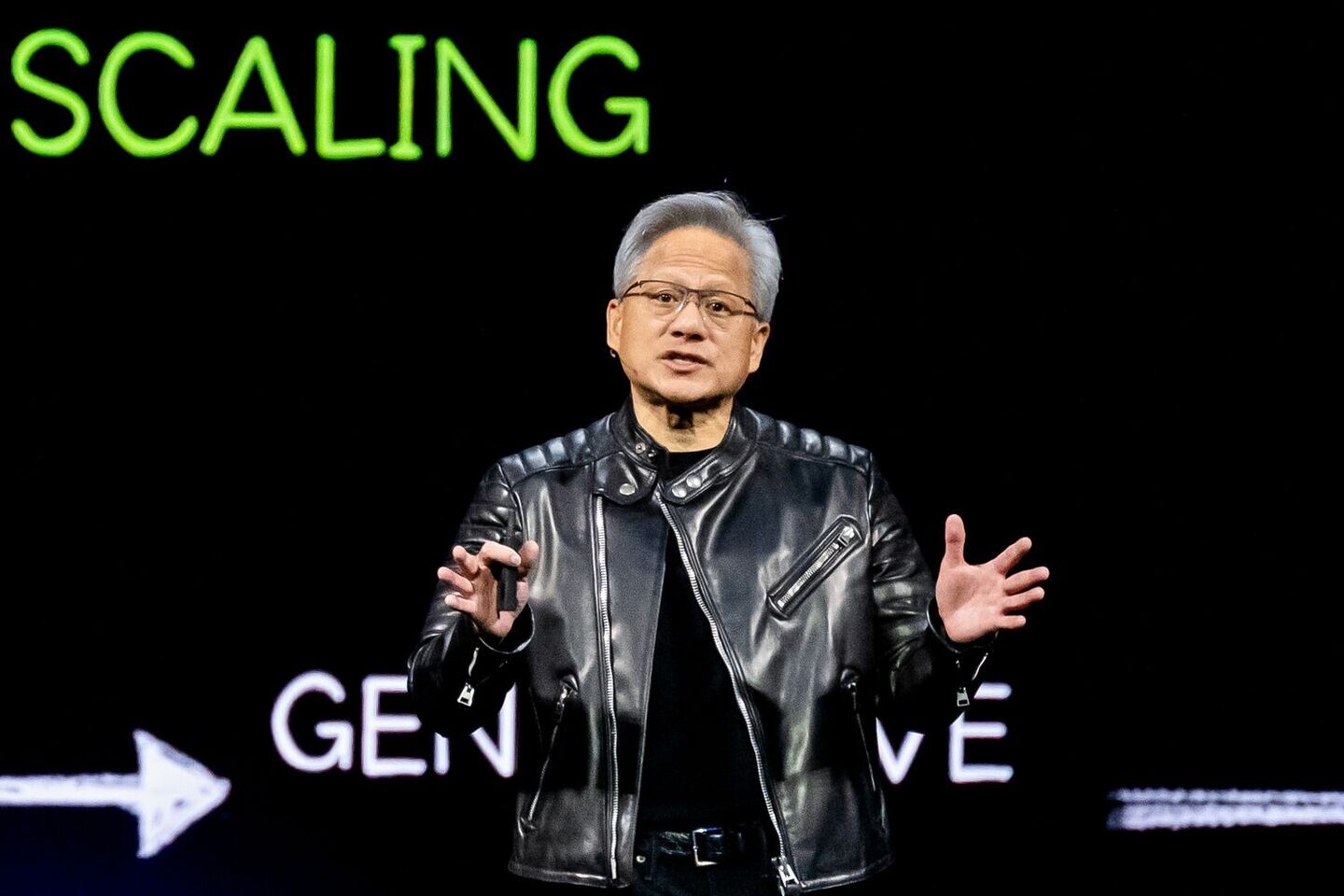
NVIDIA's CEO Jensen Huang made some interesting commentary for the Financial Times, stating that the company will procure over half a trillion US Dollars worth of electronics over the next four years, and it it plans to keep hundreds of billions from the supply chain procurement in the US. "Overall, we will procure, over the course of the next four years, probably half a trillion dollars worth of electronics in total. And I think we can easily see ourselves manufacturing several hundred billion of it here in the US," said Jensen for FT. NVIDIA currently manufactures its silicon at TSMC's facilities, as well as electronics like motherboards and servers at Foxconn. However, the geopolitical situation is making NVIDIA reconsider its supply chain dependencies, and the company is looking for more US-based manufacturing.
NVIDIA confirmed that its latest "Blackwell" series of GPUs, including the latest Blackwell Ultra, are being manufactured at TSMC's Arizona facilities. TSMC announced a $100 billion investment in its Arizona expansion, and NVIDIA is ready to take up more of TSMC's capacity to meet its ever-growing demand for GPUs. During the GTC 2025 event, Jensen noted that only four cloud service providers will use 3.6 million GPUs this year. That is without any AI labs and enterprises, which are massive consumers of GPUs (xAI only has 200,000 GPU clusters). To continue manufacturing excellence so customers won't suffer, NVIDIA is also looking at other options for supply chain manufacturing partners. Intel, the only US-based company capable of producing advanced silicon, is a potential target for NVIDIA. "We evaluate their foundry technology on a regular basis, and we are ongoing in doing that... We look for opportunities to be a customer of theirs... I have every confidence that Intel can do it," added Jensen, who also stated that NVIDIA is interested in silicon manufacturing and chip packaging services, as Intel's Foveros 3D packaging and other technologies are attractive for Team Green.
NVIDIA confirmed that its latest "Blackwell" series of GPUs, including the latest Blackwell Ultra, are being manufactured at TSMC's Arizona facilities. TSMC announced a $100 billion investment in its Arizona expansion, and NVIDIA is ready to take up more of TSMC's capacity to meet its ever-growing demand for GPUs. During the GTC 2025 event, Jensen noted that only four cloud service providers will use 3.6 million GPUs this year. That is without any AI labs and enterprises, which are massive consumers of GPUs (xAI only has 200,000 GPU clusters). To continue manufacturing excellence so customers won't suffer, NVIDIA is also looking at other options for supply chain manufacturing partners. Intel, the only US-based company capable of producing advanced silicon, is a potential target for NVIDIA. "We evaluate their foundry technology on a regular basis, and we are ongoing in doing that... We look for opportunities to be a customer of theirs... I have every confidence that Intel can do it," added Jensen, who also stated that NVIDIA is interested in silicon manufacturing and chip packaging services, as Intel's Foveros 3D packaging and other technologies are attractive for Team Green.
Industry Analyst Walks Back Claim about Apple A20 SoC Using N3P, Repredicts TSMC 2 nm
Earlier in the week, Apple specialist press outlets picked up on a noted industry analyst's technological forecast for a future iPhone processor design. Jeff Pu—of GF Industries, Hong Kong—predicted that the next-generation A20 SoC would be produced via a TSMC 3 nm (N3P) nodes process. Despite rumors of Apple gaining front row seats at the "2 nm ballgame," the partnership between fabless chip designer and foundry could potentially revisit already covered ground. The A19 chipset was previously linked to N3P (by insiders), with Pu expressing the belief that A20 would utilize the same fundamental lithographic underpinnings; albeit enhanced with TSMC's Chip on Wafer on Substrate (CoWoS) packaging technology (for AI improvements).
This morning, MacRumors followed up on their initial news article—they reported that "wires were crossed" at GF Industries, regarding projections for the (2026) iPhone 18 generation. The publication received direct feedback from the man of the hour: "Jeff Pu (lead Apple analyst) has since clarified that he believes the A20 chip will be manufactured with the N2 process, so the information about the chip using the N3P process should be disregarded. Earlier reports had said the A20 chip would be 2 nm, so rumors align again. This is ultimately good news, as it means the A20 chip should have more substantial performance and power efficiency improvements over the A19 chip." Cutting-edge smartphone processor enthusiasts expressed much disappointment when A20 was (regressively) linked to N3P; the latest revisement should instill some joy. According to industry moles, TSMC is making good progress with its cutting-edge 2 nm node process—mass production is expected to start at some point within the second half of 2025.


This morning, MacRumors followed up on their initial news article—they reported that "wires were crossed" at GF Industries, regarding projections for the (2026) iPhone 18 generation. The publication received direct feedback from the man of the hour: "Jeff Pu (lead Apple analyst) has since clarified that he believes the A20 chip will be manufactured with the N2 process, so the information about the chip using the N3P process should be disregarded. Earlier reports had said the A20 chip would be 2 nm, so rumors align again. This is ultimately good news, as it means the A20 chip should have more substantial performance and power efficiency improvements over the A19 chip." Cutting-edge smartphone processor enthusiasts expressed much disappointment when A20 was (regressively) linked to N3P; the latest revisement should instill some joy. According to industry moles, TSMC is making good progress with its cutting-edge 2 nm node process—mass production is expected to start at some point within the second half of 2025.


NVIDIA Commercializes Silicon Photonics with InfiniBand and Ethernet Switches
NVIDIA has developed co-packaged optics (CPO) technology with TSMC for its upcoming Quantum-X InfiniBand and Spectrum-X Ethernet switches, integrating silicon photonics directly onto switch ASICs. The engineering approach reduces power consumption by 3.5x. It decreases signal loss from 22 dB to 4 dB compared to traditional pluggable optics, addressing critical power and connectivity limitations in large-scale GPU deployments, especially in 10,000+ GPU systems. The architecture incorporates continuous wave laser sources within the switch chassis, consuming 2 W per port, compared to the 10 W required by conventional externally modulated lasers in pluggable modules. This configuration, combined with integrated optical engines that use 7 W versus 20 W for traditional digital signal processors, reduces total optical interconnect power from approximately 72 MW to 21.6 MW in a 400,000 GPU data center scenario.
Specifications for the Quantum 3450-LD InfiniBand model include 144 ports running at 800 Gb/s, delivering 115 Tb/s of aggregate bandwidth using four Quantum-X CPO sockets in a liquid-cooled chassis. The Spectrum-X lineup features the SN6810 with 128 ports at 800 Gb/s (102.4 Tb/s) and the higher-density SN6800 providing 512 ports at 800 Gb/s for 409.6 Tb/s total throughput. The Quantum-X InfiniBand implementation uses a monolithic switch ASIC with six CPO modules supporting 36 ports at 800 Gb/s, while the Spectrum-X Ethernet design employs a multi-chip approach with a central packet processing engine surrounded by eight SerDes chiplets. Both architectures utilize 224 Gb/s signaling per lane with four lanes per port. NVIDIA's Quantum-X switches are scheduled for availability in H2 2025, with Spectrum-X models following in H2 2026.


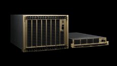
Specifications for the Quantum 3450-LD InfiniBand model include 144 ports running at 800 Gb/s, delivering 115 Tb/s of aggregate bandwidth using four Quantum-X CPO sockets in a liquid-cooled chassis. The Spectrum-X lineup features the SN6810 with 128 ports at 800 Gb/s (102.4 Tb/s) and the higher-density SN6800 providing 512 ports at 800 Gb/s for 409.6 Tb/s total throughput. The Quantum-X InfiniBand implementation uses a monolithic switch ASIC with six CPO modules supporting 36 ports at 800 Gb/s, while the Spectrum-X Ethernet design employs a multi-chip approach with a central packet processing engine surrounded by eight SerDes chiplets. Both architectures utilize 224 Gb/s signaling per lane with four lanes per port. NVIDIA's Quantum-X switches are scheduled for availability in H2 2025, with Spectrum-X models following in H2 2026.


Apple "A20" SoC Linked to TSMC "N3P" Process, AI Aspect Reportedly Improved with Advanced Packaging Tech
Over a year ago, industry watchdogs posited that Apple was patiently waiting in line at the front of TSMC's 2 Nanometer GAA "VVIP queue." The securing of cutting-edge manufacturing processes seems to be a consistent priority for the Cupertino, California-headquartered fabless chip designer. Current generation Apple chipsets—at best—utilize TSMC 3 nm (N3E) wafers. Up until very recently, many insiders believed that the projected late 2026 launch of A20 SoC-powered iPhone 18 smartphones would signal a transition to the Taiwanese foundry's advanced 2 nm (N2) node process. Officially, TSMC has roadmapped the start of 2 nm mass production around the second half of 2025.
According to Jeff Pu—a Hong Kong-based analyst at GF Securities—the speculated A20 (2026) chipset could stick with N3P. Leaks suggest that aspects of Apple's next in line "A19" and "A19 Pro" mobile SoCs could be produced via a 3 nm TSMC process. MacRumors has picked up on additional inside track whispers; about Apple M5 processors (for next-gen iPad Pro models) being based on N3P—"likely due to increased wafer costs." Pu reckons that Apple's engineering team has provisioned a major generational improvement with A20's AI capabilities, courtesy of TSMC's Chip on Wafer on Substrate (CoWoS) packaging technology. This significant upgrade is touted to tighten integration between the chip's processor, unified memory, and Neural Engine segments. Revised insider forecasts have positioned A21 chip designs as natural candidates for a shift into 2 nm GAA territories.


According to Jeff Pu—a Hong Kong-based analyst at GF Securities—the speculated A20 (2026) chipset could stick with N3P. Leaks suggest that aspects of Apple's next in line "A19" and "A19 Pro" mobile SoCs could be produced via a 3 nm TSMC process. MacRumors has picked up on additional inside track whispers; about Apple M5 processors (for next-gen iPad Pro models) being based on N3P—"likely due to increased wafer costs." Pu reckons that Apple's engineering team has provisioned a major generational improvement with A20's AI capabilities, courtesy of TSMC's Chip on Wafer on Substrate (CoWoS) packaging technology. This significant upgrade is touted to tighten integration between the chip's processor, unified memory, and Neural Engine segments. Revised insider forecasts have positioned A21 chip designs as natural candidates for a shift into 2 nm GAA territories.


Apr 16th, 2025 09:19 EDT
change timezone
Latest GPU Drivers
New Forum Posts
- Last game you purchased? (772)
- Help me identify Chip of this DDR4 RAM (20)
- 5070ti overclock...what are your settings? (5)
- Windows 11 fresh install to do list (23)
- How to relubricate a fan and/or service a troublesome/noisy fan. (229)
- GPU Memory Temprature is always high (16)
- Help For XFX RX 590 GME Chinese - Vbios (4)
- PCGH: "hidden site" to see total money spend on steam (3)
- Share your AIDA 64 cache and memory benchmark here (3053)
- NVFlash for RTX 50 Series (Blackwell) (0)
Popular Reviews
- G.SKILL Trident Z5 NEO RGB DDR5-6000 32 GB CL26 Review - AMD EXPO
- ASUS GeForce RTX 5080 TUF OC Review
- DAREU A950 Wing Review
- The Last Of Us Part 2 Performance Benchmark Review - 30 GPUs Compared
- Sapphire Radeon RX 9070 XT Pulse Review
- Sapphire Radeon RX 9070 XT Nitro+ Review - Beating NVIDIA
- Upcoming Hardware Launches 2025 (Updated Apr 2025)
- Thermaltake TR100 Review
- Zotac GeForce RTX 5070 Ti Amp Extreme Review
- TerraMaster F8 SSD Plus Review - Compact and quiet
Controversial News Posts
- NVIDIA GeForce RTX 5060 Ti 16 GB SKU Likely Launching at $499, According to Supply Chain Leak (182)
- NVIDIA Sends MSRP Numbers to Partners: GeForce RTX 5060 Ti 8 GB at $379, RTX 5060 Ti 16 GB at $429 (124)
- Nintendo Confirms That Switch 2 Joy-Cons Will Not Utilize Hall Effect Stick Technology (105)
- Over 200,000 Sold Radeon RX 9070 and RX 9070 XT GPUs? AMD Says No Number was Given (100)
- Nintendo Switch 2 Launches June 5 at $449.99 with New Hardware and Games (99)
- Sony Increases the PS5 Pricing in EMEA and ANZ by Around 25 Percent (85)
- NVIDIA PhysX and Flow Made Fully Open-Source (77)
- NVIDIA Pushes GeForce RTX 5060 Ti Launch to Mid-April, RTX 5060 to May (77)