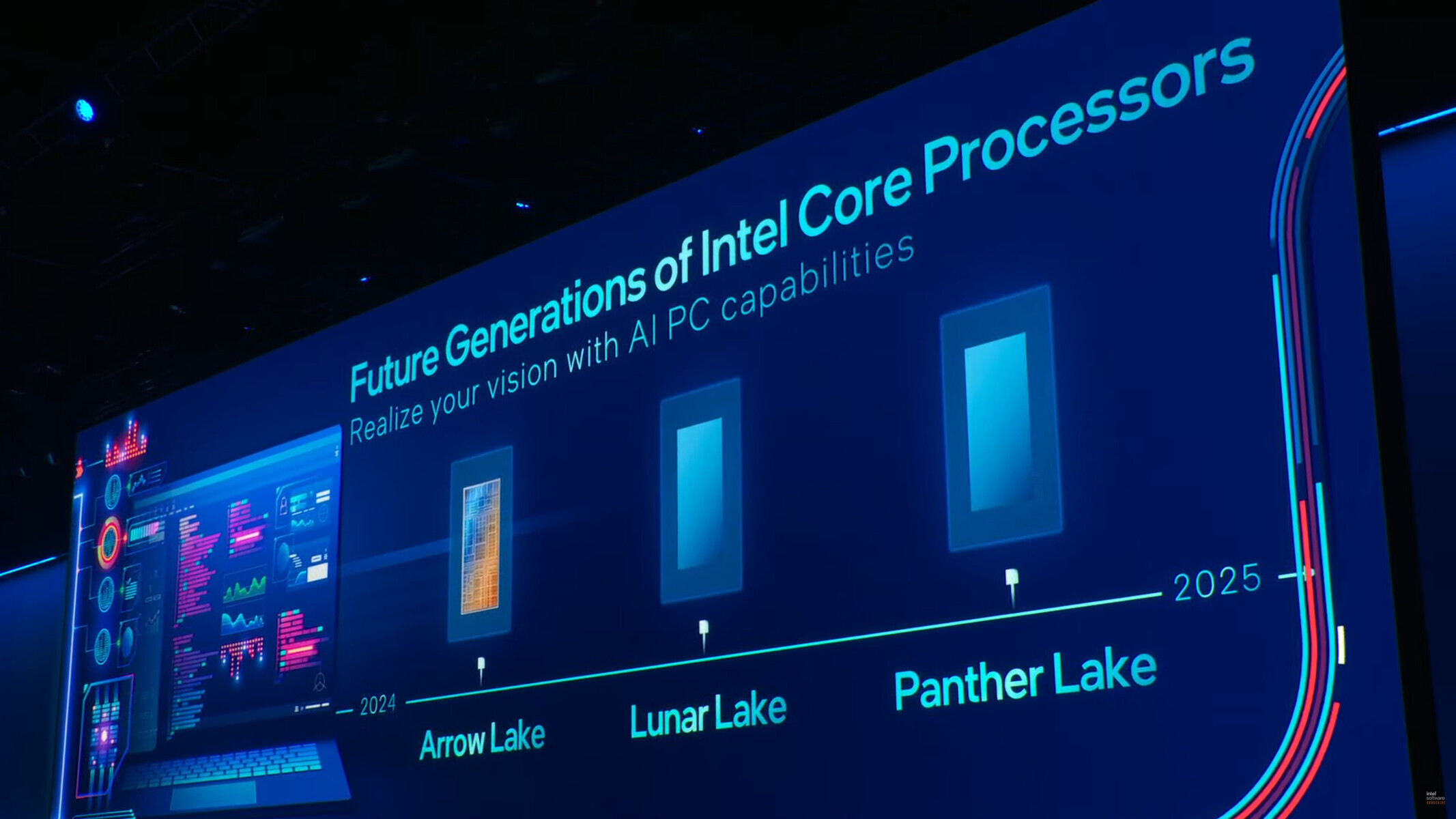
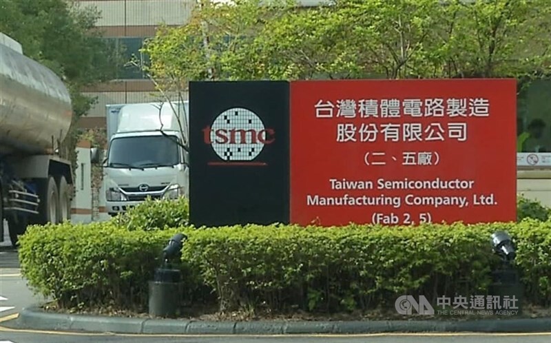
News Posts matching #TSMC

Return to Keyword Browsing

TSMC, Broadcom & NVIDIA Alliance Reportedly Set to Advance Silicon Photonics R&D

Taiwan's Economic Daily reckons that a freshly formed partnership between TSMC, Broadcom, and NVIDIA will result in the development of cutting-edge silicon photonics. The likes of IBM, Intel and various academic institutes are already deep into their own research and development processes, but the alleged new alliance is said to focus on advancing AI computer hardware. The report cites a significant allocation of—roughly 200—TSMC staffers onto R&D involving the integration of silicon photonic technologies into high performance computing (HPC) solutions. They are very likely hoping that the usage of optical interconnects (on a silicon medium) will result in greater data transfer rates between and within microchips. Other benefits include longer transmission distances and a lower consumption of power.

TSMC vice president Yu Zhenhua has placed emphasis on innovation, in a similar fashion to his boss, within the development process (industry-wide): "If we can provide a good silicon photonics integrated system, we can solve the two key issues of energy efficiency and AI computing power. This will be a new one...Paradigm shift. We may be at the beginning of a new era." The firm is facing unprecedented demand from its clients—it hopes to further expand its advanced chip packaging capacity to address these issues by late 2024. A shift away from the limitations of "conventional electric" data transmissions could bring next generation AI compute GPUs onto the market by 2025.

TSMC Prediction: AI Chip Supply Shortage to Last ~18 Months

TSMC Chairman Mark Liu was asked to comment on all things artificial intelligence-related at the SEMICON Taiwan 2023 industry event. According to a Nikkei Asia report, he foresees supply constraints lasting until the tail end of 2024: "It's not the shortage of AI chips. It's the shortage of our chip-on-wafer-on-substrate (COWOS) capacity...Currently, we can't fulfill 100% of our customers' needs, but we try to support about 80%. We think this is a temporary phenomenon. After our expansion of advanced chip packaging capacity, it should be alleviated in one and a half years." He cites a recent and very "sudden" spike in demand for COWOS, with numbers tripling within the span of a year. Market leader NVIDIA relies on TSMC's advanced packaging system—most notably with the production of highly-prized A100 and H100 series Tensor Core compute GPUs.

These issues are deemed a "temporary" problem—it could take around 18 months to eliminate production output "bottlenecks." TSMC is racing to bolster its native activities with new facilities—plans for a new $2.9 billion advanced chip packaging plant (in Miaoli County) were disclosed during summer time. Liu reckons that industry-wide innovation is necessary to meet growing demand through new methods to "connect, package and stack chips." Liu elaborated: "We are now putting together many chips into a tightly integrated massive interconnect system. This is a paradigm shift in semiconductor technology integration." The TSMC boss reckons that processing units fielding over one trillion transistors are viable within the next decade: "it's through packaging with multiple chips that this could be possible.".

MediaTek Successfully Develops First Chip Using TSMC's 3 nm Process, Set for Volume Production in 2024

MediaTek and TSMC today announced that MediaTek has successfully developed its first chip using TSMC's leading-edge 3 nm technology, taping out MediaTek's flagship Dimensity system-on-chip (SoC) with volume production expected next year. This marks a significant milestone in the long-standing strategic partnership between MediaTek and TSMC, with both companies taking full advantage of their strengths in chip design and manufacturing to jointly create flagship SoCs with high performance and low power features, empowering global end devices.

"We are committed to our vision of using the world's most advanced technology to create cutting edge products that improve our lives in meaningful ways," said Joe Chen, President of MediaTek. "TSMC's consistent and high-quality manufacturing capabilities enable MediaTek to fully demonstrate its superior design in flagship chipsets, offering the highest performance and quality solutions to our global customers and enhancing the user experience in the flagship market."

AMD's Lisa Su Endorses TSMC's Fab 21 Arizona Facility

TSMC is having a tough time getting its Phoenix, Arizona facility up to fully functional standards—large-scale production at Fab 21 has been delayed into 2025 (as announced back in July). Cited factors include workforce-related issues and sluggish installation of state-of-the-art manufacturing equipment. These setbacks are not too disconcerting in the eyes of leadership at AMD—today CEO Dr. Lisa Su declared that her firm will be one of the first in line to contract with TSMC's Fab 21, thanks to long established bonds: "I think we have gotten extremely good at managing supply chain, so I would say that is one of our core strengths. TSMC has been a phenomenal partner for us in terms of advanced technology, both on the silicon side as well as the packaging side, and we very much value that relationship." Su and NVIDIA chief Jensen Huang were key figures present at the Arizona facility's December 2022 opening ceremony.

AMD's top brass is in attendance at this year's Goldman Sachs Communacopia and Technology Conference, alongside arch rival Intel. The latter has already dropped their own revelation for the day. Su commented on North American chip manufacturing circumstances: "When you when you think about the geopolitical situation, geographic diversity is important to us...So, the Arizona factory is very important to us. We are going to be one of the early users, we are putting our first tape outs in shortly with the idea of being a significant user of Arizona. I think we will continue to look at the geographic diversity as an important piece of it." AMD has been fabless since 2009, and relies heavily on TSMC's tried and true Taiwan-based plants to produce CPU, GPU, DPU and FPGA products—it will be interesting to observe how things pan out when some of this output gets shifted over to a fledgling facility positioned out there in the Sonoran desert.

Intel Predicted to Rely on TSMC for Increased Outsourcing in 2024 & 2025

Intel's leadership has announced the hastened expansion of 20 A and 18 A-capable fabrication facilities in Arizona, in order to meet next year's anticipated manufacturing demand from Foundry Services clients. Team Blue's native efforts are possibly not enough in the eyes of an investment bank—Taiwan's Commercial Times has managed to take a look at industry analysis conducted by Goldman Sachs Securities. Intel is predicted to broaden its outsourcing to TSMC in 2024 and 2025—although a part of said report proposes the hypothetically bizarre scenario where Intel outsources all of its products at a cost of $18.6 billion in 2024, and $19.4 billion in 2025 (in terms of total addressable market). A more down-to-earth synopsis outlines TSMC winning Intel outsourcing contracts worth $5.6 billion in 2024, and $9.7 billion for 2025.

According to Trendforce's report this would approximately account: "for 6.4% and 9.4% of TSMC's overall revenue in the corresponding years." Industry analyst Andrew Lu was contacted for comment on the conjectural conditions: "(this) explains that Intel's wafer chip manufacturing division competes with TSMC, rather than its design division. The design division is striving for survival in the high-speed computing semiconductor sector, and it is currently hopeful for close collaboration with TSMC. Lu even predicts that Intel's wafer manufacturing and design divisions will inevitably be further separated into two companies several years down the line."

Top Ten Semiconductor Foundries Report a 1.1% Quarterly Revenue Decline in 2Q23, Anticipated to Rebound in 3Q23

TrendForce reports an interesting shift in the electronics landscape: dwindling inventories for TV components, along with a surging mobile repair market that's been driving TDDI demand, have sparked a smattering of urgent orders in the Q2 supply chain. These last-minute orders have served as pivotal lifelines, propping up Q2 capacity utilization and revenue for semiconductor foundries. However, the adrenaline rush from these stop-gap orders may be a short-lived phenomenon and is unlikely to be carried over into the third quarter.

On the other hand, demand for staple consumer products like smartphones, PCs, and notebooks remains sluggish, perpetuating a slump in the use of expensive, cutting-edge manufacturing processes. At the same time, traditionally stable sectors—automotive, industrial control, and servers—are undergoing inventory correction. The confluence of these trends has resulted in a sustained contraction for the world's top ten semiconductor foundries. Their global revenue declined by approximately 1.1% for the quarter, amounting to a staggering US$26.2 billion.

Intel Wants More Than its Fair Share of CHIPS Act Money

During the Aspen Security Forums 2023, Intel CEO Pat Gelsinger spoke on the topic of semiconductors and national security. During his speech, Gelsinger mentioned that Intel should get the lion's share of the US$52 billion US CHIPS Act money, simply because Intel is a US company. In Gelsinger's opinion, it appears that TSMC and Samsung don't deserve as much, despite both companies manufacturing semiconductors for US companies, with Samsung already having a foundry in Texas, while TSMC is still struggling with the construction of its Arizona foundry.

Admittedly, Intel has far more foundries in the US, but it also seems like Gelsinger forgot about other foundries, such as GlobalFoundries, but also companies such as Micron, Texas Instruments, Qorvo, NXP, On Semi, Analog Devices and so forth that all own foundries that produce their own chips on US soil. We'd expect all these companies to be eyeing the CHIPS Act cash and without many of those companies, Intel wouldn't be able to sell any of its chips, as many of them produce much needed components that are used to build motherboards, laptops and what not. Gelsinger was obviously pointing fingers at the current US China trade war and how the export controls are causing concerns with regards to the global semiconductor business. As such, Gelsinger wants Intel to have fewer restrictions from the currently imposed trade regulations, largely due to China being some 25 to 30 percent of Intel's market, with Intel being busy expanding in the country. Make what you want of this, but it's clear that Gelsinger is expecting to eat the cake and have it at the same time. Video after the break.

AMD "Navi 4C" GPU Detailed: Shader Engines are their own Chiplets

"Navi 4C" is a future high-end GPU from AMD that will likely not see the light of day, as the company is pivoting away from the high-end GPU segment with its next RDNA4 generation. For AMD to continue investing in the development of this GPU, the gaming graphics card segment should have posted better sales, especially in the high-end, which it didn't. Moore's Law is Dead scored details of what could have been a fascinating technological endeavor for AMD, in building a highly disaggregated GPU.

AMD's current "Navi 31" GPU sees a disaggregation of the main logic components of the GPU that benefit from the latest 5 nm foundry node to be located in a central Graphics Compute Die; surrounded by up to six little chiplets built on the older 6 nm foundry node, which contain segments of the GPU's Infinity Cache memory, and its memory interface—hence the name memory cache die. With "Navi 4C," AMD had intended to further disaggregate the GPU, identifying even more components on the GCD that can be spun out into chiplets; as well as breaking up the shader engines themselves into smaller self-contained chiplets (smaller dies == greater yields and lower foundry costs).

Phison Shows Its IMAGIN+ System for Flash-enabled AI+ML at FMS 2023

Phison Electronics, a global leader in NAND flash and storage solutions, announces a technology demonstration of unique customer-based solutions fully realized through the IMAGIN+ customization service at Flash Memory Summit 2023.

Phison has expanded its IMAGIN+ design service to include AI computational models and AI services solutions. Customers work with specialized Phison teams to design and engineer custom flash deployments that precisely address the data performance and endurance requirements of next generation products including those highly optimized for aiDAPTIV AI+ML workloads. With IMAGIN+ design services, Phison teams work hand-in-hand with customers to deliver AI-boosted SSD solutions that address demanding requirements.

TSMC is Building a $10B Fab In Germany

TSMC (TWSE: 2330, NYSE: TSM), Robert Bosch GmbH, Infineon Technologies AG (FSE: IFX / OTCQX: IFNNY), and NXP Semiconductors N.V. (NASDAQ: NXPI) today announced a plan to jointly invest in European Semiconductor Manufacturing Company (ESMC) GmbH, in Dresden, Germany to provide advanced semiconductor manufacturing services. ESMC marks a significant step towards construction of a 300 mm fab to support the future capacity needs of the fast-growing automotive and industrial sectors, with the final investment decision pending confirmation of the level of public funding for this project. The project is planned under the framework of the European Chips Act.

The planned fab is expected to have a monthly production capacity of 40,000 300 mm (12-inch) wafers on TSMC's 28/22 nanometer planar CMOS and 16/12 nanometer FinFET process technology, further strengthening Europe's semiconductor manufacturing ecosystem with advanced FinFET transistor technology and creating about 2,000 direct high-tech professional jobs. ESMC aims to begin construction of the fab in the second half of 2024 with production targeted to begin by the end of 2027.

China Hosts 40% of all Arm-based Servers in the World

The escalating challenges in acquiring high-performance x86 servers have prompted Chinese data center companies to accelerate the shift to Arm-based system-on-chips (SoCs). Investment banking firm Bernstein reports that approximately 40% of all Arm-powered servers globally are currently being used in China. While most servers operate on x86 processors from AMD and Intel, there's a growing preference for Arm-based SoCs, especially in the Chinese market. Several global tech giants, including AWS, Ampere, Google, Fujitsu, Microsoft, and Nvidia, have already adopted or developed Arm-powered SoCs. However, Arm-based SoCs are increasingly favorable for Chinese firms, given the difficulty in consistently sourcing Intel's Xeon or AMD's EPYC. Chinese companies like Alibaba, Huawei, and Phytium are pioneering the development of these Arm-based SoCs for client and data center processors.

However, the US government's restrictions present some challenges. Both Huawei and Phytium, blacklisted by the US, cannot access TSMC's cutting-edge process technologies, limiting their ability to produce competitive processors. Although Alibaba's T-Head can leverage TSMC's latest innovations, it can't license Arm's high-performance computing Neoverse V-series CPU cores due to various export control rules. Despite these challenges, many chip designers are considering alternatives such as RISC-V, an unrestricted, rapidly evolving open-source instruction set architecture (ISA) suitable for designing highly customized general-purpose cores for specific workloads. Still, with the backing of influential firms like AWS, Google, Nvidia, Microsoft, Qualcomm, and Samsung, the Armv8 and Armv9 instruction set architectures continue to hold an edge over RISC-V. These companies' support ensures that the software ecosystem remains compatible with their CPUs, which will likely continue to drive the adoption of Arm in the data center space.

Intel Launches Mobile Arc A570M and A530M

Without fanfare, Intel has launched two new mobile GPUs in the shape of the Arc A570M and the A530M. The Arc A570M gets 16 Xe Cores and 256 execution units, as well as four render slices and 16 RT units. The lower-end Arc A530M gets to make do with 12 Xe cores, 192 execution units, three render slices and 12 RT units, which is a smaller cut than the model name suggests. What's interesting to note here is that the Arc A570M appears to have identical hardware specs to the Arc A550M that launched in the second quarter of 2022, although as we'll see, the clock speeds and TGP differ between the parts. The Arc A570M supports 8 GB of GDDR6 memory, the same as the Arc A550M, with the Arc A530M supports 4 or 8 GB of GDDR6.

Both the Arc A570M and the A530M will get a GPU clock speed of 1,300 MHz, which is a significant boost from the Arc A550M which is plodding along at a mere 900 MHz in comparison. This makes the two newcomers Intel's third highest clocked mobile GPUs, with only the Arc A770M and Arc A370M being clocked higher. The downside of this is an increase in TGP, where the Arc A550M had a fairly reasonable TGP of 60 Watts, the Arc A530M has a TGP range of 65 to 95 Watts, while the Arc A570M extends this to 75-95 Watts. The rest of the specs appear to carry over from the Arc A550M, so the new GPUs will support up to four displays via eDP, DP 2.0 or HDMI 2.1 and the full set of video encoders and decoders are also supported. The new additions are still made using TSMC's N6 node, so what we're looking at are most likely just optimised silicon here, which has led Intel to be able to boost the clock speeds while maintaining acceptable thermals.

TSMC Inaugurates Global R&D Center, Celebrating Its Newest Hub for Technology Innovation

TSMC today held an inauguration ceremony for its global Research and Development Center in Hsinchu, Taiwan, celebrating the Company's newest hub for bringing the next generations of semiconductor technology into reality with customers, R&D partners in industry and academia, design ecosystem partners, and senior government leaders.

The R&D Center will serve as the new home for TSMC's R&D Organization, including the researchers who will develop TSMC's leading-edge process technology at the 2-nanometer generation and beyond, as well as scientists and scholars blazing the trail with exploratory research into fields such as novel materials and transistor structures. With R&D employees already relocating to their workplaces in the new building, it will be ready for its full complement of more than 7,000 staff by September 2023.

Acer Co-founder Skeptical about US Semiconductor Industry's Prospects

Stan Shih, the co-founder & honorary chairman of Acer Inc., thinks that the USA will have hard time catching up with Asian semiconductor production facilities. Yahoo Taiwan managed to extract some choice comments from the multi-faceted businessman—he believes that the US government's initiative to boost native chip making will not be enough to match existing overseas strongholds. A key area of focus was volume output—Shih reckons that North America is already too far behind Asian counterpart industries, with Acer's home base of Taiwan being particularly strong (in his opinion). Workplace culture and state of the art equipment are cited as the main pillars for success.

Shih observed that that US chip industry has historically been far too reliant on outsourcing (going back many decades) production to foreign facilities, and Asia's position has been fortified thanks to long established and optimized supply chains—he thinks that the American system is not mature enough to reach parity. On a semi-related note, TSMC is reportedly struggling to get its new US facility fully operational—company chairman Mark Liu (according to Tom's Hardware): "said that the Taiwanese company would delay mass production of its Arizona fab from early 2024 to 2025, partly due to a lack of cleanroom tools necessary to produce chips at scale." TSMC has been transferring staff from its home turf to plug staffing gaps at the Phoenix facility—Liu divulged his latest batch of complaints during an earnings conference (last Thursday): "We are encountering certain challenges, as there is an insufficient number of skilled workers with the specialized expertise required for equipment installation in a semiconductor-grade facility."

Micron Delivers Industry's Fastest, Highest-Capacity HBM to Advance Generative AI Innovation

Micron Technology, Inc. today announced it has begun sampling the industry's first 8-high 24 GB HBM3 Gen2 memory with bandwidth greater than 1.2 TB/s and pin speed over 9.2 Gb/s, which is up to a 50% improvement over currently shipping HBM3 solutions. With a 2.5 times performance per watt improvement over previous generations, Micron's HBM3 Gen2 offering sets new records for the critical artificial intelligence (AI) data center metrics of performance, capacity and power efficiency. These Micron improvements reduce training times of large language models like GPT-4 and beyond, deliver efficient infrastructure use for AI inference and provide superior total cost of ownership (TCO).

The foundation of Micron's high-bandwidth memory (HBM) solution is Micron's industry-leading 1β (1-beta) DRAM process node, which allows a 24Gb DRAM die to be assembled into an 8-high cube within an industry-standard package dimension. Moreover, Micron's 12-high stack with 36 GB capacity will begin sampling in the first quarter of calendar 2024. Micron provides 50% more capacity for a given stack height compared to existing competitive solutions. Micron's HBM3 Gen2 performance-to-power ratio and pin speed improvements are critical for managing the extreme power demands of today's AI data centers. The improved power efficiency is possible because of Micron advancements such as doubling of the through-silicon vias (TSVs) over competitive HBM3 offerings, thermal impedance reduction through a five-time increase in metal density, and an energy-efficient data path design.

Report Suggests German Government Prepping $22 Billion Aid Package for Native Chip Production

According to a report published by Bloomberg, the German government has formed plans to create €20 billion ($22 billion) of investments to aid in the growth of local semiconductor manufacturing. The article proposes that the organization is racing to bolster the country's technology sector, and is attempting to secure essential supplies of components. Various geopolitical issues have complicated matters in recent times. Funding will be made available to German and international companies, from Germany's (now diversified) Climate and Transformation reserve, over the next four years. The finance ministry responded to Bloomberg's query, and stated: "The draft for the economic plan 2024 and the financial plan until 2027 for the Climate and Transformation Fund are currently being prepared...This process has not yet been completed." Germany's economy ministry did not provide a statement/response to Bloomberg's queries.

Around 75% of the fund is reportedly set aside for multinational semiconductor firms including Intel Corporation (USA) and Taiwan Semiconductor Manufacturing Company Limited (TSMC). Bloomberg believes that Team Blue is due an allocation of €10 billion for investments in its new production facility, located close to Magdeburg, Germany. The government is allegedly deep into talks with TSMC regarding the foundation of a proposed €10 billion production base in the Dresden area—the likes of BMW, Mercedes-Benz and Volkswagen AG would benefit greatly with quicker access to (localized) microcontrollers manufacturing facilities. The government could subsidize half of that total investment (€5 billion). Infineon is possibly in line to receive a €1 billion aid package, since it is building a new fab location in Dresden.

NVIDIA is Looking at Samsung for HBM3 Memory and 2.5D Chip Packaging

According to news out of Korea, NVIDIA is considering Samsung as a partner not only for HBM3 memory, but also as a potential partner when it comes to 2.5D chip packaging. The latter is due to TSMC having limited capacity when it comes to handling all of its customers advanced chip packaging needs, although Samsung is apparently not the only potential partner NVIDIA is looking at. Taiwan based SPIL and US based Amkor Technology are two alternative candidates for the 2.5D chip packaging according to the Elec.

As far as HBM3 memory goes, NVIDIA doesn't have as many potential options, with SK Hynix being its current partner, who NVIDIA will continue to work with when it comes to HBM memory for its high-end AI accelerators and GPUs. It's likely that Samsung is trying to win NVIDIA back as a foundry customer, by proving that it's capable of handling the chip packaging for NVIDIA. Samsung will likely use its I-Cube 2.5D packaging technology and the Elec suggests that Samsung would still be using TSMC made GPU wafers which will be mated with Samsung HMB3 memory. Samsung has as yet not started its mass production of HMB3 memory, but have sampled customers with evaluation samples that are said to have received very positive feedback. For now, nothing has been agreed and TSMC is, as we know, looking to expand its 2.5D packaging business by over 40 percent, but the question is how quickly TSMC can move before its customers consider other competitors.

Samsung Claims Higher 3 nm Yields than TSMC

Competition between Samsung and TSMC in the 4 nm and 3 nm foundry process markets is about to heat up, with the Korean foundry claiming yields competitive to those of TSMC, according to a report in the Kukmin Ilbo, a Korean daily newspaper. 4 nm is the final silicon fabrication process to use the FinFET technology that powered nodes ranging between 16 nm to 4 nm. Samsung Foundry is claiming 4 nm wafer yields of 75%, against the 80% yields figure put out by TSMC. 4 nm powers several current-generation mobile SoCs, PC processors, and more importantly, the GPUs driving the AI gold-rush.

Things get very interesting with 3 nm, the node that debuts GAA-FET (gates all around FET) technology. Here, Samsung claims to offer higher yields than TSMC, with its 3 nm GAA node clocking 60% yields, against 55% put out by TSMC. Samsung was recently bitten by a scandal where its engineers allegedly falsified yields figures to customers to score orders, which had a cascading effect on the volumes and competitiveness of their customers. We're inclined to think that Samsung has taken lessons and is more careful with the yields figures being reported in the press. Meanwhile, Intel Foundry Services competes with the Intel 3 node, which is physically 7 nm FinFET, but with electrical characteristics comparable to those of 3 nm.

Major Foundries Not Too Concerned About China's Restrictions on Rare Metal Exports

China announced on Monday (June 3) that it would restrict exports of two rare metals——both crucial materials in the computer chip manufacturing process. The nation's Ministry of Commerce stated that their new measures were necessary to "safeguard national security and interests". The Chinese government is contending with several sanctions from Western countries—most notably their access to advanced semiconductor manufacturing equipment is now heavily controlled. Reuters has contacted a number of foundries about the potential impact of rare material shipment limitations. Taiwan Semiconductor Manufacturing Company (TSMC) has shrugged it off as a minor inconvenience, their spokesperson stated: "After evaluation, we do not expect the export restrictions on raw materials gallium and germanium will have any direct impact on TSMC's production. We will continue to monitor the situation closely."

WIN Semiconductors Corp—a Taiwanese firm that specializes in the provision of gallium arsenide wafers—informed the news agency about its low-level reliance on Chinese mineral sources. They are able to sidestep and procure gallium and germanium from suppliers located in Germany, Japan, and North America. The Japanese Semiconductor Equipment Association stated that it was too early to tell whether China's export restrictions will result in material shortages. Supply chains could be disrupted to some degree due to China controlling over 90% of the world's gallium and germanium production, but DigiTimes Asia proposes that new sanctions will not prohibit production and export activities. According to experts in the field supply lines will continue to operate, with buyers required to jump through some extra hoops in order to gain approval for certain market segments. The purification of gallium and germanium is mostly controlled by American and Japanese entities—the processed form of these metals is used in semiconductor production—DigiTimes reckons that these firms will probably feel the initial impact of new trade restrictions.

Apple Reported to be Reducing Factory Output of Vision Pro AR Headset

The Financial Times believes that Apple is running into major production issues related to its Vision Pro mixed reality headset—insider sources claim that the mega-sized multinational technology company is adjusting internal sales goals for the $3499 AR/VR "spatial computer." Leadership had set an ambitious internal target of 1 million units sold in 2024, but the complexity of the system's design has apparently caused major setbacks for manufacturing partners. Apple is reported to have signed up with Luxshare, a Chinese contract manufacturer, to assemble Vision Pro headsets—insiders within both organizations reckon that only 400,000 units will be ready for sale throughout 2024. This number seems to be fairly optimistic given that Trendforce predicted that a mere 200,000 would be shipped next year.

FT gathered information from two other sources placed within the Chinese supply chain—they claim that Apple and Luxshare could encounter major component shortages in 2024, resulting in a production shortfall—with an estimated 130,000 to 150,000 finalized units. The article points out that the most complex (and costly) aspect of the headset lies in its micro-OLED display setup, that also includes outward facing lenses. TSMC and Sony are reported to be the suppliers of these parts (as featured on the prototypes), but Apple is allegedly not satisfied with low production numbers, and not enough batches are "free of defects." A cheaper version of the Vision Pro is apparently now on the backburner, since Apple is unlikely to recoup—factoring in R&D expenses—within the first year of the intial product's launch.

TSMC Said to Start Construction of 1.4 nm Fab in 2026

According to Taiwanese media, TSMC will start production of its first 1.4 nm fab in 2026, with chip production in the fab said to start sometime in 2027 or 2028. The new fab will be located in Longtan Science Park outside of Hsinchu in Taiwan, where many of TSMC's current fabs are located. TSMC is currently constructing a 2 nm and below node R&D facility at a nearby plot of land to where the new fab is expected to be built. This facility is expected to be finished in 2025 and TSMC has been allocated a total area of just over 158 hectares of land for future expansion in the area.

In related news, TSMC is expected to be charging US$25,000 per 2 nm GAA wafer, which is an increase of about a fifth compared to its 3 nm wafers which are going for around US$20,000. This is largely due to the nodes being fully booked and TSMC being able to charge a premium for its cutting edge nodes. TSMC is also expanding in CoWoS packaging facilities due to increased demand from both AMD and NVIDIA for AI related products. Currently TSMC is said to be able to output 12,000 CoWoS wafers per month and this is twice as much as last year, yet TSMC is unable to meet demand from its customers.

Major CSPs Aggressively Constructing AI Servers and Boosting Demand for AI Chips and HBM, Advanced Packaging Capacity Forecasted to Surge 30~40%

TrendForce reports that explosive growth in generative AI applications like chatbots has spurred significant expansion in AI server development in 2023. Major CSPs including Microsoft, Google, AWS, as well as Chinese enterprises like Baidu and ByteDance, have invested heavily in high-end AI servers to continuously train and optimize their AI models. This reliance on high-end AI servers necessitates the use of high-end AI chips, which in turn will not only drive up demand for HBM during 2023~2024, but is also expected to boost growth in advanced packaging capacity by 30~40% in 2024.

TrendForce highlights that to augment the computational efficiency of AI servers and enhance memory transmission bandwidth, leading AI chip makers such as Nvidia, AMD, and Intel have opted to incorporate HBM. Presently, Nvidia's A100 and H100 chips each boast up to 80 GB of HBM2e and HBM3. In its latest integrated CPU and GPU, the Grace Hopper Superchip, Nvidia expanded a single chip's HBM capacity by 20%, hitting a mark of 96 GB. AMD's MI300 also uses HBM3, with the MI300A capacity remaining at 128 GB like its predecessor, while the more advanced MI300X has ramped up to 192 GB, marking a 50% increase. Google is expected to broaden its partnership with Broadcom in late 2023 to produce the AISC AI accelerator chip TPU, which will also incorporate HBM memory, in order to extend AI infrastructure.

AMD Zen 4c Not an E-core, 35% Smaller than Zen 4, but with Identical IPC

AMD on Tuesday (June 13) launched the EPYC 9004 "Bergamo" 128-core/256-thread high density compute server processor, and with it, debuted the new "Zen 4c" CPU microarchitecture. A lot had been made out about Zen 4c in the run up to yesterday's launch, such as rumors that it is a Zen 4 "lite" core that has lesser number-crunching muscle, and hence lower IPC, and that Zen 4c is AMD's answer to Intel's E-core architectures, such as "Gracemont" and "Crestmont." It turns out that it's neither a lite version of Zen 4, nor is it an E-core, but a physically compacted version of the Zen 4 core, with identical number crunching machinery.

First things first—Zen 4c has the same exact IPC as Zen 4 (that's performance at a given clock-speed). This is because its front-end, execution stage, load/store component, and internal cache hierarchy is exactly the same. It has the same 88-deep load queue, 64-deep store queue, the same 675,000 µop cache, the exact same INT+FP issue width of 10+6, the same exact INT register file, the same scheduler, and cache latencies. The L1I and L1D caches are the same 32 KB in size as "Zen 4," and so is the dedicated L2 cache, at 1 MB.

Top 10 Foundries Report Nearly 20% QoQ Revenue Decline in 1Q23, Continued Slide Expected in Q2

TrendForce reports that the global top 10 foundries witnessed a significant 18.6% QoQ decline in revenue during the first quarter of 2023. This decline—amounting to approximately US$27.3 billion—can be attributed to sustained weak end-market demand and the compounded effects of the off-peak season. The rankings also underwent notable changes, with GlobalFoundries surpassing UMC to secure the third position, and Tower Semiconductor surpassing PSMC and VIS to claim the seventh spot.

Declining capacity utilization rate and shipment volume contribute to widened revenue decline
The revenue decline in Q1 was primarily influenced by declining capacity utilization rates and shipment volume across the top 10 foundries. For instance, TSMC generated US$16.74 billion in revenue—marking a 16.2% QoQ drop in revenue. Weakened demand for mainstream applications such as laptops and smartphones led to a significant decline in the utilization rates and revenue of the 7/6 nm and 5/4 nm processes, falling over 20% and 17%, respectively. While the second quarter may see temporary relief coming from rush orders, the persistently low capacity utilization rate indicates that revenue is likely to continue declining, albeit at a slower pace compared to Q1.

U.S. Government to Allow Chipmakers to Expand Facilities in China

The United States government has imposed sanctions on companies exporting their goods to China with the aim of limiting the country's technological advancements. This forced many companies to reduce their shipments of the latest technologies; however, according to the latest information from The Wall Street Journal, the Biden administration will allow companies to keep expanding their production capacities in China. As the source notes, quoting statements from government officials, the top semiconductor makers such as Samsung, SK Hynix, and TSMC, all of which have a chip production facility in China, will be allowed to expand the production capacity without any US backlash.

Of course, this does not contradict the plan of a US export-control policy, which the administration plans to continue. Alan Estevez, undersecretary of commerce for industry and security, noted last week in the industry gathering that the US plans to continue these restrictions for another year. Reportedly, all manufacturers of wafer fab equipment (WFE) from the US must acquire an export license from the Department of Commerce before exporting any tools for making either logic of memory chip indented for customers in China. Chipmakers Samsung, SK Hynix, and TSMC all received their licenses to export from October 2022 to October 2023. However, the US government now allows these companies to continue upgrading their Chinese plans beyond the renewed license expiry date of October 2024.
Return to Keyword Browsing
May 19th, 2024 02:41 EDT change timezone

New Forum Posts

Popular Reviews

Controversial News Posts