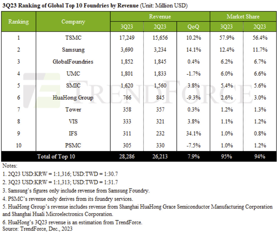
AI Datacenters Warming Up to Instinct CDNA Causes AMD Stock to Hit Near Record High
With NVIDIA's Ampere and Hopper GPUs enjoying a domination in the AI acceleration industry, compute companies are turning to AMD's Instinct CDNA series accelerators to look for alternatives. It seems like they've found one. This has financial market analysts excited, causing the AMD company stock to hit near record highs. AMD recently launched the Instinct MI300X and MI300A processors based on the CDNA 3 architecture, which the company claims beat NVIDIA's H100 "Hopper" processors at competitive prices, which has encouraged analysts from major financial institutions, including Barclays, KeyBanc Capital, and Susquehanna Financial Group, to increase their price targets for the AMD stock. As of market closure at Jan 17, 7:59:56 PM UTC, the AMD stock stood at $160.17, near its November 2021 record high of $164.46.
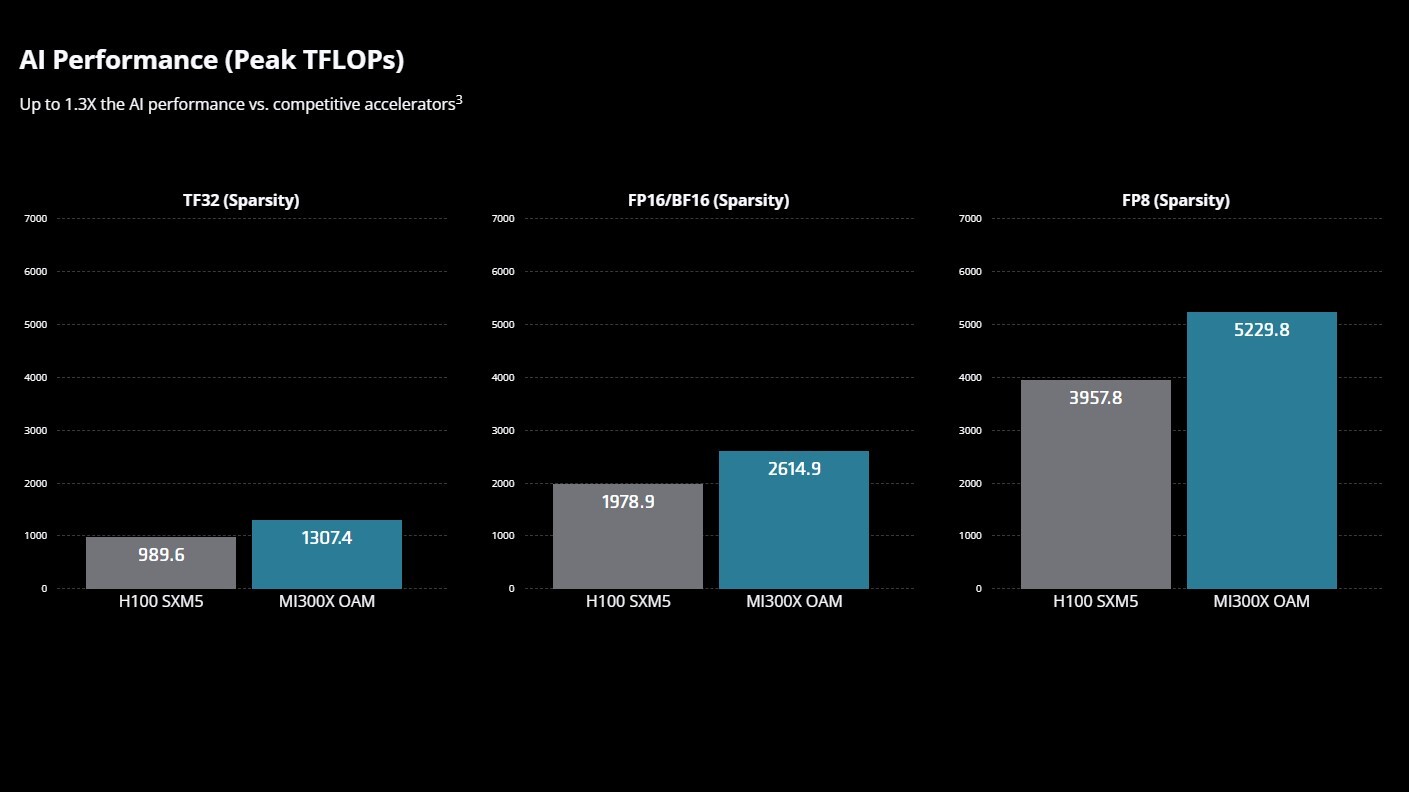
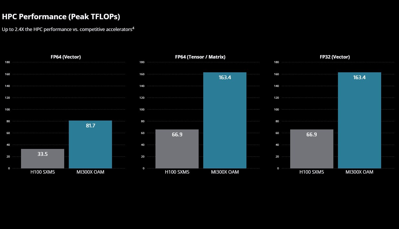
AMD's data center business looks to ramp up Instinct CDNA accelerators through 2024. These large chiplet-based GPUs are based on the same 5 nm TSMC foundry nodes to NVIDIA's H100 "Hopper," and to maximize the use of its foundry allocation, it's been reported that AMD might even forego large gaming GPUs based on its Radeon RX RDNA4 architecture, to maximize its allocation for high-margin CDNA3 chips. The Instinct MI300X features a colossal 304 compute units worth 19,456 stream processors capable of AI-relevant math formats, and 192 GB of 8192-bit HBM3 memory, with 5.2 TB/s of memory bandwidth on tap.


AMD's data center business looks to ramp up Instinct CDNA accelerators through 2024. These large chiplet-based GPUs are based on the same 5 nm TSMC foundry nodes to NVIDIA's H100 "Hopper," and to maximize the use of its foundry allocation, it's been reported that AMD might even forego large gaming GPUs based on its Radeon RX RDNA4 architecture, to maximize its allocation for high-margin CDNA3 chips. The Instinct MI300X features a colossal 304 compute units worth 19,456 stream processors capable of AI-relevant math formats, and 192 GB of 8192-bit HBM3 memory, with 5.2 TB/s of memory bandwidth on tap.