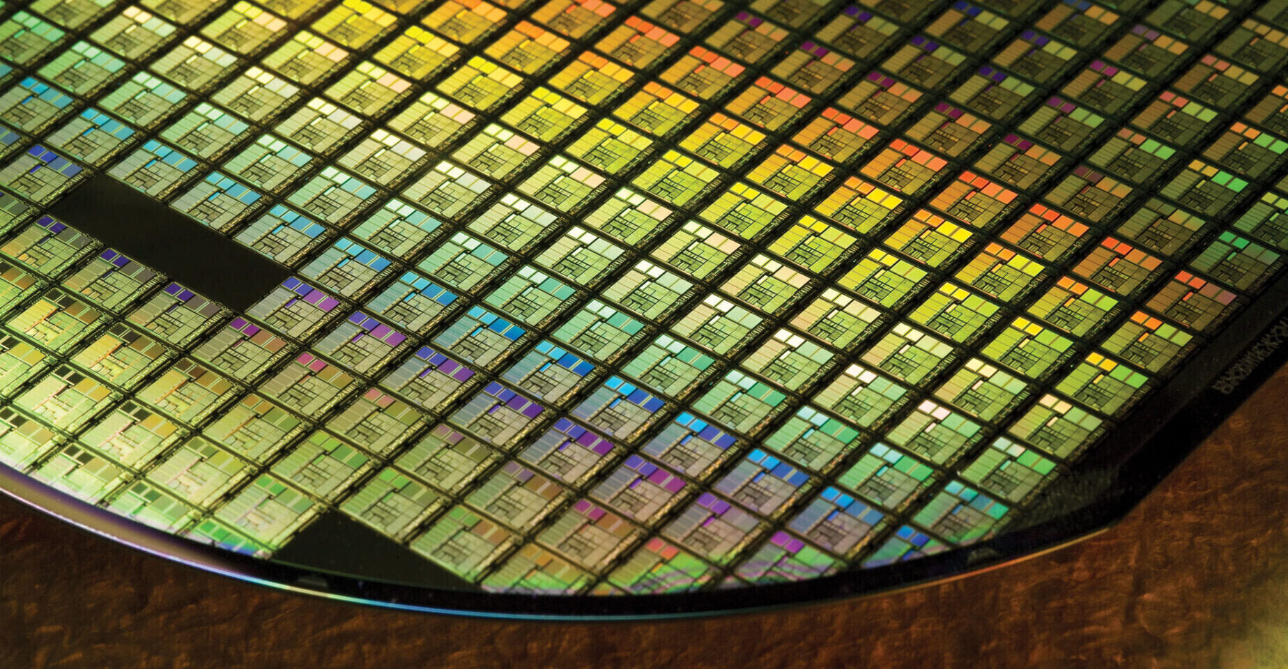
US Exempts Semiconductors From Taiwan Tariffs, But Chip-Making Equipment Remains on the List
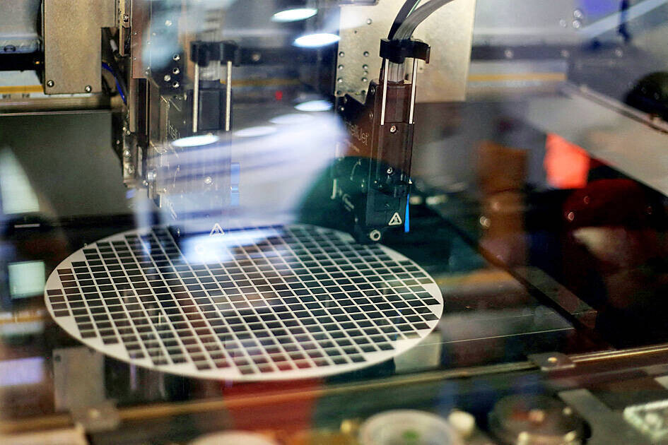
Yesterday, United States President Donald Trump announced a set of tariffs imposed on US trading partners, imposing a series of 10%+ tariffs on partners, calling it a "Liberation Day." Today, we are calculating how much these tariffs will impact consumers and what is most important at TechPowerUp: semiconductors powering our GPUs and CPUs. According to one of the top investment banks, Goldman Sachs, semiconductors are exempt from the reciprocal tariffs that Trump has imposed on Taiwan. However, the semiconductor manufacturing equipment used by makers like TSMC is not exempt and is expected to be hit with the 32% tariffs. This is only half of what Taiwan imposes on imports of US-made goods. For TSMC, the number one maker of GPUs and CPUs, tariffs can be tricky to navigate. While its existing manufacturing facilities use equipment sourced from Dutch ASML and a few US companies like Lam Research and KLA Corporation, it shouldn't be a problem to ship new silicon to the US.
However, if TSMC wants to expand its manufacturing facilities in any country that is not the US, it will have to deal with 32% tariffs on US-sourced silicon manufacturing equipment. For EU-based ASML, things are looking a little different. If over 20% of the equipment is made up of US content, a tariff exemption might apply, potentially reducing import costs. If more than one-fifth of a product's components or value originates from US sources, the equipment may be eligible for tariff relief. ASML's machines include some US components, so determining whether these machines meet the 20% threshold is crucial. If they do, the tariff exemption could help lower costs associated with importing these advanced machines, reaching up to $380 million. For non-US-injected goods, EU entities are subject to 20% tariffs.
However, if TSMC wants to expand its manufacturing facilities in any country that is not the US, it will have to deal with 32% tariffs on US-sourced silicon manufacturing equipment. For EU-based ASML, things are looking a little different. If over 20% of the equipment is made up of US content, a tariff exemption might apply, potentially reducing import costs. If more than one-fifth of a product's components or value originates from US sources, the equipment may be eligible for tariff relief. ASML's machines include some US components, so determining whether these machines meet the 20% threshold is crucial. If they do, the tariff exemption could help lower costs associated with importing these advanced machines, reaching up to $380 million. For non-US-injected goods, EU entities are subject to 20% tariffs.