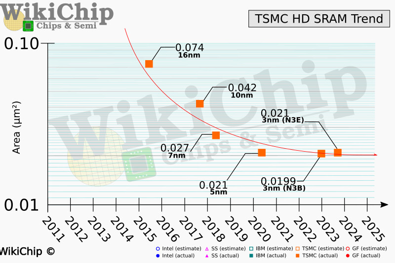
News Posts matching #TSMC

Return to Keyword Browsing

Intel's Next Generation GPUs to be Made by TSMC, Celestial Set for 3 nm Process

Intel has awarded TSMC with some big contracts for future manufacturing of next generation GPUs, according to Taiwan's Commercial Times. As previously covered on TPU, the second generation Battlemage graphics processing units will get fabricated via a 4 nm process. According to insider sources at both partnering companies, Intel is eyeing a release date in the second half of 2024 for this Xe2-based architecture. The same sources pointed to the third generation Celestial graphics processing units being ready in time for a second half of 2026 launch window. Arc Celestial, which is based on the Xe3 architecture, is set for manufacture in the coming years courtesy of TSMC's N3X (3 nm) process node.

One of the sources claim that Intel is quietly confident about its future prospects in the GPU sector, despite mixed critical and commercial reactions to the first generation line-up of Arc Alchemist discrete graphics cards. The company is said to be anticipating great demand for more potent versions of its graphics products in the future, and internal restructuring efforts have not dulled the will of a core team of engineers. The restructuring process resulted in the original AXG graphics division being divided into two sub-groups - CCG and DCAI. The pioneer of the entire endeavor, Raja Koduri, departed Intel midway through last month, to pursue new opportunities with an AI-focused startup.

CHIPS Act Requirements Untenable According to Silicon Manufacturers in South Korea and Taiwan

Silicon manufacturers in South Korea and Taiwan have questioned the requirements outlined in the United States Chips and Science Act - South Korean President Yoon Suk Yeol spoke on Thursday March 30, and said that there was a growing concern within companies Samsung Electronics Corporation and SK Hynix Inc. with regard to criteria for new U.S. semiconductor subsidies. Excess profit sharing is one area of contention, as the U.S. government will expect dividends to be paid under special conditions. The companies are also reluctant to meet the requirements of submitting detailed information about fab capacity and yield estimates. Leaders are pointing to the potential sensitive nature of exposing too much confidential corporate strategy to bodies in the USA, and sources within Samsung and SK Hynix are worried that budgetary planning information will be revealed in minute detail.

The CHIPS Act grants a $52 billion pool of research and manufacturing funds, and subsidies would be sourced from it. SK Hynix's parent group is considering an application in order to gain access to funding via the CHIPS Act, the SK Group has formed plans to invest $15 billion of its own money into the U.S. chip manufacturing sector - a North American location for an advanced chip packaging plant is being decided upon. Samsung has invested a substantial $25 billion into its Texas operation, so is eligible to receive U.S. government subsidies as well.

AMD Speeds Up Development of "Zen 5" to Thwart Intel Xeon "Emerald Rapids"?

In no mood to cede its market-share growth to Intel, AMD has reportedly decided to accelerate the development of its next-generation "Zen 5" microarchitecture for debut within 2023. In its mid-2022 presentations, AMD had publicly given "Zen 5" a 2024 release date. This is part of a reading-in-between the lines for a recent GIGABYTE press release announcing server platforms powered by relatively low-cost Ryzen desktop processors. The specific sentence from that release reads "The next generation of AMD Ryzen desktop processors that will come out later this year will also be supported on this AM5 platform, so customers who purchase these servers today have the opportunity to upgrade to the Ryzen 7000 series successor."

While the GIGABYTE press release speaks of a next-generation Ryzen desktop processor, it stands to reason that it is referencing an early release of "Zen 5," and since AMD shares the CPU complex dies (CCDs) between its Ryzen client and EPYC server processors, the company is looking at a two-pronged upgrade to its processor lineup, with its next-generation EPYC "Turin" processor competing with Xeon Scalable "Emerald Rapids," and Ryzen "Granite Ridge" desktop processors taking on Intel's Core "Raptor Lake Refresh" and "Meteor Lake-S" desktop processors. It is rumored that "Zen 5" is being designed for the TSMC 3 nm node, and could see an increase in CPU core count per CCD, up from the present 8. TSMC 3 nm node goes into commercial mass-production in the first half of 2023 as the TSMC N3 node, with a refined N3E node slated for the second half of the year.

Huawei Reportedly Develops Chip Design Tools for 14 nm and Above

Amid the US sanctions, Chinese technology giant Huawei has reportedly developed tools to create processors with 14 nm and above lithography. According to Chinese media Yicai, Huawei and its semiconductor partners have teamed up to create replacement tools in place of US chip toolmakers like Cadence, Synopsys, and Mentor/Siemens. These three companies control all of the world's Electronic Design Automation (EDA) tools used for every step of chip design, from architecture to placement and routing to the final physical layout. Many steps need to be taken before making a tapeout of a physical chip, and Huawei's newly developed EDA tools will help the Chinese industry with US sanctions which crippled Huawei for a long time.

Having no access to US-made chipmaking tools, Huawei has invested substantial time into making these EDA tools. However, with competing EDA makers supporting lithography way below 14 nm, Huawei's job still needs to be completed. Chinese semiconductor factories are currently capable of 7 nm chip production, and Huawei itself is working on making a sub-7 nm EUV scanner to aid manufacturing goals and compete with the latest from TSMC and other. If Huawei can create EUV scanners that can achieve transistor sizes smaller than 7 nm, we expect to see their EDA tools keep pace as well. It is only a matter of time before they announce adaptation for smaller nodes.

2026 All-Time High in Store for Global 300 mm Semiconductor Fab Capacity After 2023 Slowdown

Semiconductor manufacturers worldwide are forecast to increase 300 mm fab capacity to an all-time high of 9.6 million wafers per month (wpm) in 2026, SEMI announced today in its 300 mm Fab Outlook to 2026 report. After strong growth in 2021 and 2022, the 300 mm capacity expansion is expected to slow this year due to soft demand for memory and logic devices.

"While the pace of the global 300 mm fab capacity expansion is moderating, the industry remains squarely focused on growing capacity to meet robust secular demand for semiconductors," said Ajit Manocha, SEMI President and CEO. "The foundry, memory and power sectors will be major drivers of the new record capacity increase expected in 2026."

Intel Arc "Battlemage" to Double Shader Count, Pack Larger Caches, Use TSMC 4 nm

Intel's next-generation Arc "Battlemage" GPU is expected to numerically-double its shader counts, according to a report by RedGamingTech. The largest GPU from the Arc "Battlemage" series, the "BMG-G10," aims to power SKUs that compete in the performance segment. The chip is expected to be built on a TSMC 4 nm-class EUV node, similar to NVIDIA's GeForce "Ada" GPUs, and have a die-size similar to that of the "AD103" silicon powering the GeForce RTX 4080.

Among the juiciest bits from this report are that the top "Battlemage" chip will see its Xe Core count doubled to 64, up from 32 on the top "Alchemist" part. This would see its execution unit (EU) count doubled to 1,024, and unified shader counts at 8,192. Intel is expected to give the chip clock speeds in excess of 3.00 GHz. The Xe Cores themselves could see several updates, including IPC uplifts, and support for new math formats. The memory sub-system is expected to see an overhaul, with a large 48 MB on-die L2 cache. While the memory bus is unchanged at 256-bit wide, the memory speed could see a significant increase up from the 16-17.5 Gbps on the Arc A770. As for when customers can actually expect products, the RedGamingTech report puts launch of the Arc "Battlemage" series at no sooner than Q2-2024. The company is expected to launch refreshed "Alchemist+" GPUs in 2023.

Apple A17 Bionic SoC Performance Targets Could be Lowered

Apple's engineering team is rumored to be adjusting performance targets set for its next generation mobile SoC - the A17 Bionic - due to issues at the TSMC foundry. The cutting edge 3 nm process is proving difficult to handle, according to industry tipsters on Twitter. The leaks point to the A17 Bionic's overall performance goals being lowered by 20%, mainly due to the TSMC N3B node not meeting production targets. The factory is apparently lowering its yield and execution targets due to ongoing problems with FinFET limitations.

The leakers have recently revealed more up-to-date A17 Bionic's Geekbench 6 scores, with single thread performance at 3019, and multi-thread at 7860. Various publications have been hyping the mobile SoC's single thread performance as matching that of desktop CPUs from Intel and AMD, more specifically 13th-gen Core i7 and 'high-end' Ryzen models. Naturally the A17 Bionic cannot compete with these CPUs in terms of multi-thread performance.

NVIDIA, ASML, TSMC and Synopsys Set Foundation for Next-Generation Chip Manufacturing

NVIDIA today announced a breakthrough that brings accelerated computing to the field of computational lithography, enabling semiconductor leaders like ASML, TSMC and Synopsys to accelerate the design and manufacturing of next-generation chips, just as current production processes are nearing the limits of what physics makes possible.

The new NVIDIA cuLitho software library for computational lithography is being integrated by TSMC, the world's leading foundry, as well as electronic design automation leader Synopsys into their software, manufacturing processes and systems for the latest-generation NVIDIA Hopper architecture GPUs. Equipment maker ASML is working closely with NVIDIA on GPUs and cuLitho, and is planning to integrate support for GPUs into all of its computational lithography software products.

Samsung Preps Mass Production of Third-Generation 4 nm Chipsets, Start Date Expected Mid-2023

In a Samsung Electronics business report released on March 12, it was revealed that the giant electronics manufacturer will begin mass production of new chips through a 4 nm 2.3-generation process. The newly established manufacturing process is set to start by the end of H1 2023, which means that mid-June would be the expected commencement date. Samsung Semiconductor has managed to produce a satisfactory yield of wafers with the new generation chipsets.

Samsung Electronics has experienced significant problems with the production of previous generation 4 nm chips, and industry insiders have been surprised by the sudden announcement of the third generation version, given rumors pointing to the Hwaseong factory struggling to reach yields at the 60% mark. Qualcomm famously dropped Samsung in favor of TSMC as a source of 4 nm chipsets in 2022, due to disappointing yield figures.

Report: Total Revenue of Top 10 Foundries Fell by 4.7% QoQ for 4Q22 and Will Slide Further for 1Q23

According to TrendForce's latest survey of the global foundry market, electronics brands began adjusting their inventories in 2Q22, but foundries were unable to rapidly adapt to this development because they reside in the more upper portion of the supply chain. Moreover, revising procurement quantities of long-term foundry contracts takes time as well. Hence, only some tier-2 and -3 foundries were able to immediately respond to the changes in their clients' demand. Also, among them, 8-inch wafer foundries made a more pronounced reduction in their capacity utilization rates. As for the remaining foundries, the downward corrections that they made to their capacity utilization rates did not become noticeable until 4Q22. Hence, in 4Q22, the quarterly total revenue of the global top 10 foundries registered a QoQ decline for the first time after 13 consecutive quarters of positive growth. The quarterly total revenue of the top 10 foundries came to US$33,530 million, reflecting a drop of 4.7% from 3Q22. Moving into 1Q23, TrendForce projects that the quarterly total revenue of the top 10 will show an even steeper drop on account of seasonality and the uncertain macroeconomic situation.

TSMC's 3 nm Node at Near 50 Percent Utilisation, Other Nodes Seeing Lower Demand

Based on multiple reports out of Taiwan, TSMC is seeing increased utilisation of its 3 nm node and its production line is now at close to 50 percent utilisation. The main customer here is without a doubt Apple and TSMC is churning out some 50-55,000 wafers a month on its 3 nm node. TSMC is also getting ready to start production on its N3E node later this year, which will see some customers move to the node.

However, it's not all good news, as TSMC is seeing a decline in utilisation on its 5/4 and 7/6 nm nodes as demand has dropped significantly here, with different news outlets reporting different figures. Some are suggesting the 7/6 nm nodes might have dropped as low as to 50 percent utilisation, others mention 70 percent. The 5/4 nm nodes aren't anywhere nearly as badly affected and remain at around 80 percent utilisation. The good news for TSMC is that this is expected to be a temporary slump in demand and most of its leading edge nodes should be back at somewhere around a 90 percent utilisation rate by the second half of the year. However, this depends on what the demand for its partners' products will look like going forward, as many of TSMC's customers are seeing lower demand for their products in turn.

Samsung Hires ex TSMC Executive to Improve Advanced IC Packaging

Business Korea got the scoop on Samsung hiring an ex TSMC executive by the name of Lin Jun-Cheng, who was with TSMC for almost 19 years. His role at Samsung will be as VP of Samsung's advanced packaging business, something he should be more than familiar with, as during his time at TSMC, he was part of no less than 450 patents involving chip packaging. Lin has also worked for Micron and more recently for a company called Skytech, that specialises in advanced IC packaging equipment.

Samsung has relied on third parties when it comes to more advanced chip packaging and has been behind Intel and TSMC in this area. The Business Korea article mentions that Samsung has been spending a lot of resources over the past year to build its own advanced packaging business, including hiring industry experts. Samsung has hired ex Apple, Intel and Qualcomm staff to join or head various teams related to its foundry division, not only for packaging, but also experts in various lithography processes, such as EUV. Samsung is clearly taking its foundry business seriously, even though they have had their fair share of issues with various customers over the past few years.

TSMC Said to be Planning Second Fab in Japan

The rumour mill has kicked into high gear this week about TSMC planning a second fab in Japan. The original source is the Nikkan Kogyo newspaper (via Reuters), based in Tokyo, although it's unclear where the actual fab would be located, if it's indeed even happening. According to the paper, the new fab would be focusing on 5 and 10 nanometer chips, but production isn't expected to start until sometime in the second half of this decade. This suggests that these would be mainstream nodes by then, which points to yet another fab for either the vehicle industry or something similar.

The fab is said to cost more than a trillion yen, or over US$7.4 billion to build. TSMC's CEO C.C. Wei was asked about the potential fab during TSMC's latest earnings call, but simply said that the company had nothing further to add. TSMC is of course busy building a fab in Japan on Kyushu island, but as it'll have a node capacity for 12 to 16 nm parts, it makes sense that TSMC would already be planning for an extension of said fab that can produce on more advanced nodes as its customers will be moving to more advanced nodes over time.

AMD Expected to Occupy Over 20% of Server CPU Market and Arm 8% in 2023

AMD and Arm have been gaining up on Intel in the server CPU market in the past few years, and the margins of the share that AMD had won over were especially large in 2022 as datacenter operators and server brands began finding that solutions from the number-2 maker growing superior to those of the long-time leader, according to Frank Kung, DIGITIMES Research analyst focusing primarily on the server industry, who anticipates that AMD's share will well stand above 20% in 2023, while Arm will get 8%.

Prices are one of the three major drivers that resulted in datacenter operators and server brands switching to AMD. Comparing server CPUs from AMD and Intel with similar numbers of cores, clockspeed, and hardware specifications, the price tags of most of the former's products are at least 30% cheaper than the latter's, and the differences could go as high as over 40%, Kung said.

Intel Defers 3 nm Wafer Orders with TSMC, Pushes "Arrow Lake" Rollout to 2025?

Intel has reportedly deferred its orders for 3 nm wafers with TSMC, sources in PC makers tell Taiwan-based industry observer DigiTimes. Built on the TSMC N3 node, the wafers were supposed to power the Graphics tiles (containing the iGPU), of the upcoming "Arrow Lake" processors, which were originally on course for a 2024 release. The DigiTimes report detailing this development says that Intel's 3 nm wafer orders have been deferred to Q4-2024, which would realistically mean a 2025 launch for whatever product was designed to use 3 nm tiles. Advance orders for next-gen wafers by high-volume clients such as Intel, are usually placed several quarters in advance, so the foundry could suitably scale up its capacity.

MediaTek Launches Dimensity 7200 to Amplify Gaming and Photography Smartphone Experiences

MediaTek today announced the Dimensity 7200, its inaugural chipset in the new Dimensity 7000 series. The Dimensity 7200 boasts cutting-edge AI imaging features, powerful gaming optimizations, and impressive 5G speeds, all with deeply engrained power savings for extended battery life.

The Dimensity 7200 delivers the same TSMC 4 nm second-generation process found in the Dimensity 9200, and is ideal for ultra-slim designs in a variety of form factors. The octa-core CPU integrates two Arm Cortex-A715 cores, featuring operating speeds of up to 2.8 GHz, with six Cortex-A510 cores, so users can effortlessly multitask and take advantage of peak performance in every app. To further optimize power and performance, MediaTek's built-in AI Processing Unit (APU) maximizes the efficiency of AI tasks and AI-fusion processing.

Intel Meteor Lake to Feature 50% Increase in Efficiency, 2X Faster iGPU

Intel's upcoming Meteor Lake processor family is supposedly looking good with the new performance/efficiency targets. According to the @OneRaichu Twitter account, we have a potential performance estimate for the upcoming SKUs. As the latest information notes, Intel's 14th-generation Meteor Lake will feature around a 50% increase in efficiency compared to the 13th-generation Raptor Lake designs. This means that the processor can use half the power at the same performance target at Raptor Lake, increasing efficiency. Of course, the design also offers some performance improvements besides efficiency that are significant and are yet to be shown. The new Redwood Cove P-cores will be combined with the new Crestmont E-cores for maximum performance inside U/P/H configurations with 15-45 Watt power envelopes.

For integrated graphics, the source notes that Meteor Lake offers twice the performance of iGPU found on Raptor Lake designs. Supposedly, Meteor Lake will feature 128 EUs running 2.0+GHz compared to 96 EUs found inside Raptor Lake. The iGPU architecture will switch from Intel Iris to Xe-LPG 'Xe-MTL' family on the 14th gen models, confirming a giant leap in performance that iGPU is supposed to experience. Using the tile-based design, Intel combines the Intel 4 process for the CPU tile and the TSMC 5 nm process for the GPU tile. Intel handles final packaging for additional tuning, and you can see the separation below.

Intel Foundry Services Onboards a Fabless Customer, Deal Expected to Fetch over $4 Billion

Intel Foundry Services, the semiconductor foundry business of Intel, has onboarded an undisclosed fabless customer, the company disclosed in its Q4-2022 Financial Results presentation. This signals that the company wants to serve the semiconductor manufacturing industry beyond its own products, and scale up to demands, just like TSMC, UMC, Samsung Foundry, or other such semiconductor foundries do. The customer is looking to build chips on the Intel 3 foundry-node, which is rumored to offer performance/Watt and transistor-density figures comparable to TSMC 4N (4 nm EUV). Intel will extensively use Tower Semiconductor's silicon fabrication IP in the deal. Throughout its manufacturing lifecycle (from risk production to mass-production and completion), the deal is expected by Intel to generate over $4 billion in revenue for the company.
Image Courtesy: VideoCardz

Intel Xeon "Sapphire Rapids" to be Quickly Joined by "Emerald Rapids," "Granite Rapids," and "Sierra Forest" in the Next Two Years

Intel's server processor lineup led by the 4th Gen Xeon Scalable "Sapphire Rapids" processors face stiff competition from AMD 4th Gen EPYC "Genoa" processors that offer significantly higher multi-threaded performance per Watt on account of a higher CPU core-count. The gap is only set to widen, as AMD prepares to launch the "Bergamo" processor for cloud data-centers, with core-counts of up to 128-core/256-thread per socket. A technologically-embattled Intel is preparing quick counters as many as three new server microarchitecture launches over the next 23 months, according to Intel, in its Q4-2022 Financial Results presentation.

The 4th Gen Xeon Scalable "Sapphire Rapids," with a core-count of up to 60-core/120-thread, and various application-specific accelerators, witnessed a quiet launch earlier this month, and is shipping to Intel customers. The company says that it will be joined by the Xeon Scalable "Emerald Rapids" architecture in the second half of 2023; followed by "Granite Rapids" and "Sierra Forest" in 2024. Built on the same LGA4677 package as "Sapphire Rapids," the new "Emerald Rapids" MCM packs up to 64 "Raptor Cove" CPU cores, which support higher clock-speeds, higher memory speeds, and introduce the new Intel Trust Domain Extensions (TDX) instruction-set. The processor retains the 8-channel DDR5 memory interface, but with higher native memory speeds. The chip's main serial interface is a PCI-Express Gen 5 root-complex with 80 lanes. The processor will be built on the last foundry-level refinement of the Intel 7 node (10 nm Enhanced SuperFin); many of these refinements were introduced with the company's 13th Gen Core "Raptor Lake" client processors.

Foundry Revenue is Forecasted to Drop by 4% YoY for 2023, TrendForce Notes

TrendForce's recent analysis of the foundry market reveals that demand continues to slide for all types of mature and advanced nodes. The major IC design houses have cut wafer input for 1Q23 and will likely scale back further for 2Q23. Currently, foundries are expected to maintain a lower-than-ideal level of capacity utilization rate in the first two quarters of this year. Some nodes could experience a steeper demand drop in 2Q23 as there are still no signs of a significant rebound in wafer orders. Looking ahead to the second half of this year, orders will likely pick up for some components that underwent an inventory correction at an earlier time. However, the state of the global economy will remain the largest variable that affect demand, and the recovery of individual foundries' capacity utilization rates will not occur as quickly as expected. Taking these factors into account, TrendForce currently forecasts that global foundry revenue will drop by around 4% YoY for 2023. The projected decline for 2023 is more severe when compared with the one that was recorded for 2019.

Phison E26 Controller Powering Several Upcoming PCIe Gen 5 NVMe SSDs Detailed

At the 2023 International CES, we caught a hold of Phison, makes or arguably the most popular SSD controllers, which sprung to prominence on being the first to market with PCIe Gen 4 NVMe controllers, and now hopes to repeat it with PCIe Gen 5. We'd been shown a reference-design Phison E26-powered M.2 SSD, along with some hardware specs of the controller itself. The drive itself isn't much to look at—a standard looking M.2-2280 drive with a PCI-Express 5.0 x4 host interface, and the Phison E26 controller with its shiny IHS being prominently located next to a DDR4 memory chip, and two new-generation Micron Technology 3D NAND flash memory chips.

The Phison E26 controller, bearing the long-form model number PS5026-E26, is an NVMe 2.0 spec client-segment SSD controller. It has been built on the TSMC 12 nm FinFET silicon-fabrication node. The controller features an integrated DRAM controller with support for DDR4 and LPDDR4 memory types for use as DRAM cache. Its main flash interface is 8-channel with 32 NAND chip-enable (CE) lines, support for TLC and QLC NAND flash, a dual-CPU architecture, and hardware-acceleration for AES-256, TCG-Opal, and Pyrite. The controller features Phison's 5th generation LPDC ECC and internal RAID engines. For its reference-design 2 TB TLC-based drive, Phison claims sequential transfer rates of up to 13.5 GB/s reads, with up to 12 GB/s writes. The 4K random-access performance is rated at up to 1.5 million IOPS reads, with up to 2 million IOPS writes.

AMD Ryzen 7040 Series "Phoenix Point" Mobile Processor I/O Detailed: Lacks PCIe Gen 5

The online datasheets of some of the first AMD Ryzen 7040 series "Phoenix Point" mobile processors went live, detailing the processor's I/O feature-set. We learn that AMD has decided to give PCI-Express Gen 5 a skip with this silicon, at least in its mobile avatar. The Ryzen 7040 SoC puts out a total of 20 PCI-Express Gen 4 lanes, all of which are "usable" (i.e. don't count 4 lanes toward chipset-bus). This would mean that the silicon has a full PCI-Express 4.0 x16 interface for discrete graphics, and a PCI-Express 4.0 x4 link for a CPU-attached M.2 NVMe slot; unlike the "Raphael" desktop MCM and the "Dragon Range" mobile MCM, whose client I/O dies put out a total of 28 Gen 5 lanes (24 usable, with x16 PEG + two x4 toward CPU-attached M.2 slots).

Another interesting aspect about "Phoenix Point" is its memory controllers. The SoC features a dual-channel (four sub-channel) DDR5 memory interface, besides support for LPDDR5 and LPDDR5x. DDR5-5600 and LPDDR5-7600 are the native speeds supported. What's really interesting is the maximum amount of memory supported, which stands at 256 GB—double that of "Raphael" and "Dragon Range," which top out at 128 GB. This bodes well for the eventual Socket AM5 APUs AMD will design based on the "Phoenix Point" silicon. Older Ryzen 5000G "Cezanne" desktop APUs are known for superior memory overclocking capabilities to 5000X "Vermeer," with the monolithic nature of the silicon favoring latencies. Something similar could be expected from "Phoenix Point."

Top 10 TSMC Customers Said to have Cut Orders for 2023

On the day of TSMC's celebration of the mass production start of its 3 nm node, news out of Taiwan suggests that all of its top 10 customers have cut their orders for 2023. However, the cuts are unlikely to affect its new node, but rather its existing nodes, with the 7 and 6 nm nodes said to be hit the hardest, by as much as a 50 percent utilisation reduction in the first quarter of 2023. The 28 nm and 5 and 4 nm nodes are also said to be affected, although it's unclear by how much at this point in time.

Revenue is expected to fall by at least 15 percent in the first quarter of 2023 for TSMC, based on numbers from DigiTimes. The fact that TSMC has increased its 2023 pricing by six percent should at least help offset some of the potential losses for the company, but it all depends on the demand for the rest of the year. Demand for mobile devices is down globally, which is part of the reason why so many of TSMC's customers have cut back their orders, as Apple, Qualcomm and Mediatek all produce their mobile SoCs at TSMC. Add to this that the demand for computers and new computer components are also down, largely due to the current pricing and TSMC is in for a tough time next year.

TSMC Holds 3nm Volume Production and Capacity Expansion Ceremony, Marking a Key Milestone for Advanced Manufacturing

TSMC today held a 3 nanometer (3 nm) Volume Production and Capacity Expansion Ceremony at its Fab 18 new construction site in the Southern Taiwan Science Park (STSP), bringing together suppliers, construction partners, central and local government, the Taiwan Semiconductor Industry Association, and members of academia to witness an important milestone in the Company's advanced manufacturing.

TSMC has laid a strong foundation for 3 nm technology and capacity expansion, with Fab 18 located in the STSP serving as the Company's GIGAFAB facility producing 5 nm and 3 nm process technology. Today, TSMC announced that 3 nm technology has successfully entered volume production with good yields, and held a topping ceremony for its Fab 18 Phase 8 facility. TSMC estimates that 3 nm technology will create end products with a market value of US$1.5 trillion within five years of volume production.

TSMC to Mark 3 nm Mass Production Start, Looking at Potential New Fabs in Japan and Germany

According to news out of Taiwan, TSMC will hold a ceremony to mark the official mass production start of its 3 nm node on the 29th of December. This is said to help "shatter doubts about de-Taiwanization" or in simpler terms, that Taiwan will lose its golden goose as TSMC invests abroad. The 3 nm fab—known as fab 18—is based in southern Taiwan's Tainan and the ceremony also marks the start of an expansion of TSMC's most advanced fab. TSMC is said to be kicking off its N3E node production sometime in the second half of 2023, followed by its N3P node in 2024, all of which should take place at fab 18, which also produces 5 nm wafers.

In related news, according to Reuters, a Japanese lawmaker from the ruling party has said that TSMC is considering a second plant in Japan, in addition to its current joint venture that is already under construction. TSMC's response to Reuters was that the company isn't ruling out Japan for future fabs, but that the company doesn't have any current plans. At the same time, TSMC is said to be sending executives to Dresden, Germany in early 2023, for a second round of talks about building a fab to help support the European auto industry, although this would be a 28/22 nm fab, which is far from cutting edge these days, although a lot more advanced than most fabs making chips for the auto industry.
Return to Keyword Browsing
Jul 15th, 2024 23:18 EDT change timezone

New Forum Posts

Popular Reviews

Controversial News Posts