Friday, February 14th 2025

AMD Zen 6 Powers "Medusa Point" Mobile and "Olympic Ridge" Desktop Processors
AMD is readying two important client segment processors powered by the next-generation "Zen 6" microarchitecture, according to a sensational new report by Moore's Law is Dead. These are the "Medusa Point" mobile processor, and the "Olympic Ridge" desktop. The former is a BGA roughly the size and Z-Height of the current "Strix Point," but the latter is being designed for the existing Socket AM5, making it the third (and probably final) microarchitecture to do so. If you recall, Socket AM4 served three generations of Zen, not counting the refreshed "Zen+." At the heart of the effort is a new CPU complex die (CCD) that AMD plans to use across its client and server lineup.
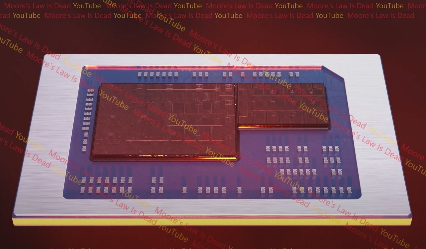
The "Zen 6" performance CCD is being designed for a 3 nm-class node, likely the TSMC N3E. This node promises a significant increase in transistor density, power, and clock speed improvements over the current TSMC N4P node being used to build the "Zen 5" CCD. Here's where it gets interesting. The CCD contains twelve full-sized "Zen 6" cores, marking the first increase in core-counts of AMD's performance cores since its very first "Zen" CCD. All 12 of these cores are part of a single CPU core complex (CCX), and share a common L3 cache. There could be a proportionate increase in cache size to 48 MB. AMD is also expected to improve the way the CCDs communicate with the I/O die and among each other.


 Going all the way back to the Ryzen 3000 series "Matisse," the two CCDs on the client desktop processor have had Infinity Fabric links to the I/O die, but no direct high-bandwidth interconnects between the two CCDs. For threads to migrate between cores of the two CCDs, they would have to make a round-trip through the main memory. AMD is looking to solve this with the introduction of a new low-latency bridge connection between the two CCDs. If the goal is to enable threads to seamlessly migrate among cores of the two CCDs, cutting out round-trips to the main memory, then the purpose of this bridge interconnect is to establish cache coherency between the two CCDs. This would vastly lower intercore latency.
Here's where things get very interesting. Apparently, the "Medusa Point" mobile processor is chiplet-based, and will use a single 12-core "Zen 6" chiplet, with a large mobile client I/O die built on an older node, likely the N4P. This mobile cIOD will contain an updated iGPU that's powered by the newer RDNA 4 graphics architecture. It will also contain the chip's memory controllers, and an updated NPU. We hope AMD works to increase the number of PCIe lanes put out by this I/O die, or at least update it to PCIe Gen 5. Pictures show small rectangular structures on the mobile client I/O die causing some speculation that it is some kind of low power island CCX with "Zen 6c" cores, although MLID lays this to rest by saying that these are workgroup processors (WGPs) of the iGPU. There are eight of these and a large slab of L2 cache, which seems to confirm that the iGPU is based on the RDNA 4 graphics architecture, and has 16 compute units (CU).
Since AMD is using the same CCD for "Medusa Point" as the "Olympic Ridge" desktop processor, you could expect variants of "Medusa Point" with 3D V-Cache. The 3D V-Cache technology is expected to be implemented on "Zen 6" much in the same way it is on "Zen 5," with an upside-down stacking—3D V-Cache die (L3D) below, with CCD on top.
Given the increase in CPU core counts, especially with "Olympic Ridge" getting up to 24 cores with two CCDs, and the inter-CCD bridge interconnect for cache coherency, AMD is going to need a new client I/O die for desktop. We've already discussed this in older articles. The new cIOD is expected to be built on the Samsung 4LPP (4 nm EUV) foundry node, which offers improvements over the TSMC N6 DUV node the current cIOD is being built on. A key area of focus for AMD will be the memory controllers, which will be updated to support higher DDR5 memory speeds using technologies such as CKD. You can currently run a "Granite Ridge" processor with memory speeds of up to DDR5-8000 but using a 1:2 clock divider is engaged between FCLK and MCLK, with 1:1 speeds being limited to around DDR5-6400. The new memory controllers will look to increase speeds with 1:1, and unlock speeds beyond 10000 MT/s with 1:2.
Then there's the matter of AI acceleration, and the new cIOD will present AMD with the opportunity to implement at least a 50 TOPS-class XDNA 2 NPU. Intel received flack for giving its "Arrow Lake" processors a 16 TOPS-class NPU that doesn't meet Copilot+ requirements, and the company is probably working to fix this in "Panther Lake," and so if AMD decides to implement an NPU on the cIOD for "Olympic Ridge," we predict it will be at least 50 TOPS-class.
Source:
Moore's Law is Dead
The "Zen 6" performance CCD is being designed for a 3 nm-class node, likely the TSMC N3E. This node promises a significant increase in transistor density, power, and clock speed improvements over the current TSMC N4P node being used to build the "Zen 5" CCD. Here's where it gets interesting. The CCD contains twelve full-sized "Zen 6" cores, marking the first increase in core-counts of AMD's performance cores since its very first "Zen" CCD. All 12 of these cores are part of a single CPU core complex (CCX), and share a common L3 cache. There could be a proportionate increase in cache size to 48 MB. AMD is also expected to improve the way the CCDs communicate with the I/O die and among each other.


Here's where things get very interesting. Apparently, the "Medusa Point" mobile processor is chiplet-based, and will use a single 12-core "Zen 6" chiplet, with a large mobile client I/O die built on an older node, likely the N4P. This mobile cIOD will contain an updated iGPU that's powered by the newer RDNA 4 graphics architecture. It will also contain the chip's memory controllers, and an updated NPU. We hope AMD works to increase the number of PCIe lanes put out by this I/O die, or at least update it to PCIe Gen 5. Pictures show small rectangular structures on the mobile client I/O die causing some speculation that it is some kind of low power island CCX with "Zen 6c" cores, although MLID lays this to rest by saying that these are workgroup processors (WGPs) of the iGPU. There are eight of these and a large slab of L2 cache, which seems to confirm that the iGPU is based on the RDNA 4 graphics architecture, and has 16 compute units (CU).
Since AMD is using the same CCD for "Medusa Point" as the "Olympic Ridge" desktop processor, you could expect variants of "Medusa Point" with 3D V-Cache. The 3D V-Cache technology is expected to be implemented on "Zen 6" much in the same way it is on "Zen 5," with an upside-down stacking—3D V-Cache die (L3D) below, with CCD on top.
Given the increase in CPU core counts, especially with "Olympic Ridge" getting up to 24 cores with two CCDs, and the inter-CCD bridge interconnect for cache coherency, AMD is going to need a new client I/O die for desktop. We've already discussed this in older articles. The new cIOD is expected to be built on the Samsung 4LPP (4 nm EUV) foundry node, which offers improvements over the TSMC N6 DUV node the current cIOD is being built on. A key area of focus for AMD will be the memory controllers, which will be updated to support higher DDR5 memory speeds using technologies such as CKD. You can currently run a "Granite Ridge" processor with memory speeds of up to DDR5-8000 but using a 1:2 clock divider is engaged between FCLK and MCLK, with 1:1 speeds being limited to around DDR5-6400. The new memory controllers will look to increase speeds with 1:1, and unlock speeds beyond 10000 MT/s with 1:2.
Then there's the matter of AI acceleration, and the new cIOD will present AMD with the opportunity to implement at least a 50 TOPS-class XDNA 2 NPU. Intel received flack for giving its "Arrow Lake" processors a 16 TOPS-class NPU that doesn't meet Copilot+ requirements, and the company is probably working to fix this in "Panther Lake," and so if AMD decides to implement an NPU on the cIOD for "Olympic Ridge," we predict it will be at least 50 TOPS-class.
90 Comments on AMD Zen 6 Powers "Medusa Point" Mobile and "Olympic Ridge" Desktop Processors
For mobile I can understand it to keep power low-er.
I'll upgrade to the Zen 6 Ryzen 9 "10950X3D" CPU (or however they'll name it), when that will be out.
As for N2 tile, I think it is for Zen 7 to be relaased somwhere in 2027, as demand for N2 wafers will be high (Apple, QLC, Intel), so price and availability will be difficult for AMD throughout 2026.
Now we get this. This will make all the people that believed the narrative about the 7900X3D and 20 nano seconds being a killer. It also seems that X3D has been a greater success than even AMD expected. It has killed the sales of the rest of them but the 7900 is still a great buy.
I also appreciate that my MB and RAM will be just fine for Zen 6. You can call me a fan boy all you want but in the CPU space AMD earns it's position with real innovation in the Space.
If nothing else, Conky will look sweet with 48 CPU utilisation graphs.
I've also heard that Apple might not pay for exclusive early access to N2. And I've heard that N2 is a bigger leap over N3 than N3 is over N5/N4, and that companies are considering skipping from N5/N4 to N2.
As for the inter CCD communication, strix point should be out soon and it can easily extrapolate what a exponentially faster inter CCD latency does to performance. For most productivity apps, don't expect too much. For games that cross codes? Expect a big jump but games shouldn't cross it anyway, especially with 12 cores. I'm wondering if they're going to use a variant of their fanout links that they favour in various capacities.
Too early to call it, but the performance jump should be akin to zen 2 > 3, with 1.5x cores.
Slapping 2 laptop CPUs together to make a 16th Gen desktop CPU is a very cruel joke.
Same source says that desktop CCDs will be 2nm.
If that’s the case I don’t see the point of using Zen6c on desktop where you have power headroom (220-230W) to implement even 24 full Zen6 cores.
They may have the IPC and efficiency advantage over Intel, but they're really behind in terms of core counts. And future Intel generations are expected to have some crazy configurations like 16P+32E.
Currently, one GMI3 link, a tad above PCIe 5.0 speed, supports theoretical maximum of 72 GB/s (16x36Gbps/8).
For Zen6, one GMI4 link, close to PCIe 6.0 speed, should support theoretical minimum of 128 GB/s (16x64Gbps/8).They are not "behind" because 16 cores provide overall higher performance in applications on 9950X than 24 cores on 285K. Also, 8 core 9800X3D is significantly faster in gaming than 24 core 285K. So, it's nonsense to say that they are "behind" in core count. It's not about core count.
Increasing core count to 24 on Zen6 will give 48 threads. They seem confident enough that this would be sufficient to counter alleged 52 single threaded cores on Nova Lake.
So 'if' Intel does manage to get near the projected performance increases that leaks seem to be leaning towards for Coyote Cove & Arctic Wolf then I actually Nova Lake could take a sizable lead against even a 24c/48t Zen 6 CPU in productivity, I am pretty sure AMD will still hold the gaming crown fairly easily with their X3D chips plus I am really not a lover of the whole P-core/E-core thing. So many times Windows has moved a heavy workload onto my E-cores just because I've minimised the window so I can get on with something else only to realise it's progressing incredibly slowly so I have to leave it on full screen behind what I am now working on just to get it to work properly so I would likely still choose a 24 core Zen 6 CPU just because of that. But it would be great to see Intel catch up or take the lead in some scenarios if nothing else to bring some competition back to the market.
If we do some napkin maths on the possible performance and said:
1 x Zen 6 core = 100 'performance points'
1 x Coyote Cove core = 100 performance points
1 x Arctic Wolf core = 40 performance points
So Zen 6 with 24 cores = 24 x 100 = 2400
Nova Lake = 16 x 100 + 32 x 40 = 2800 (a 17% increase)
Obviously these numbers are just rough educated projections based on current leaks and rumours of Zen 6 is maybe getting a 10-15% IPC improvement over Zen 5 and Coyote Cove is possibly getting a 15-20% increase over Lion Cove. Zen 6 has multi threading of course which helps it a lot but Coyote Cove is mean to be getting a bigger IPC increase plus Arctic Wolf is rumoured to be possibly getting a massive 40-50% IPC increase over Skymont so possibly only giving them 40 'performance points' might be selling them short. But the point is it's still a bit of a guessing game at the moment and it's been a very long time since Intel managed to deliver well on anything so I'm not holding my breath they will with Nova Lake but I'm crossing my fingers it could finally get very interesting in the CPU market with Intel winner in productivity with a 52 core Nova Lake CPU but with AMD almost certainly still keeping the gaming crown!
2. Imagine retail price of 52 core CPU ??? Ouch.
3. If AMD feels threathened by Nova Lake, they can create a halo SKU 12 C-core +16 c-core, which would bring 28 cores and 56 threads.