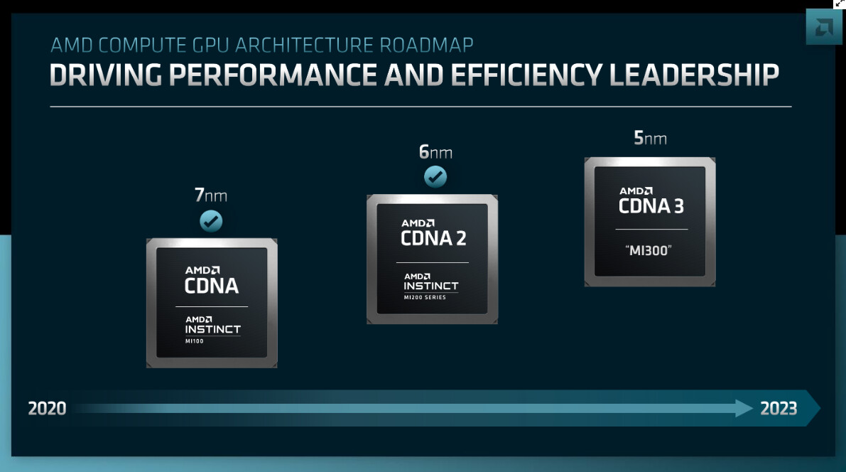
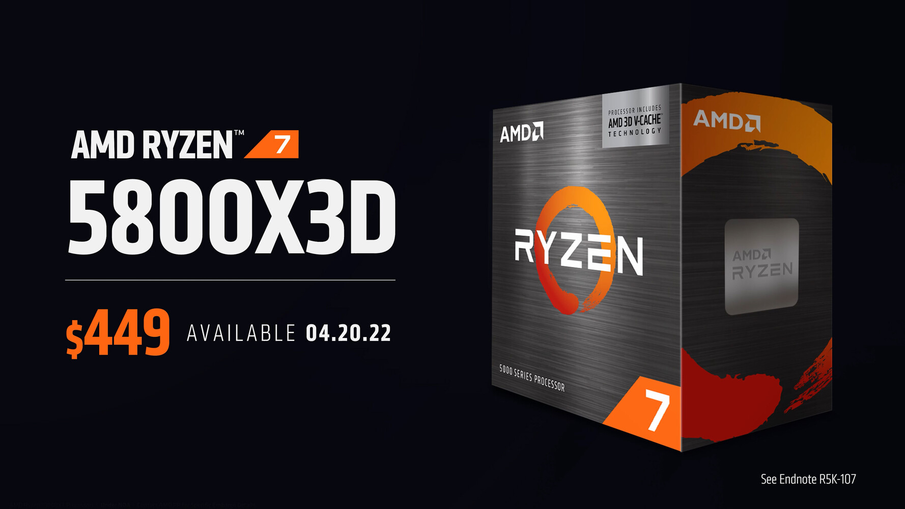
AMD Debuts Ryzen AI Max Series "Strix Halo" SoC: up to 16 "Zen 5" cores, Massive iGPU
AMD at the 2025 International CES debuted the Ryzen AI Max 300 series of mobile processors. These chips are designed to go up against the Apple M4 Pro, or the chip that powers the Apple MacBook Pro. The idea behind it is to provide leadership CPU and graphics performance from a single package, minimizing the PCB footprint from having a discrete GPU. In stark contrast, the Intel Core Ultra 200V "Lunar Lake," is designed more to go against the Apple M4, or the chips that power the latest MacBook Air but not quite the MacBook Pro. What sets "Strix Halo" functionally apart from "Lunar Lake" or even the M4 Pro, is that the AMD chip doesn't have memory-on-package (MoP), it relies on discrete LPDDR5X memory chips.
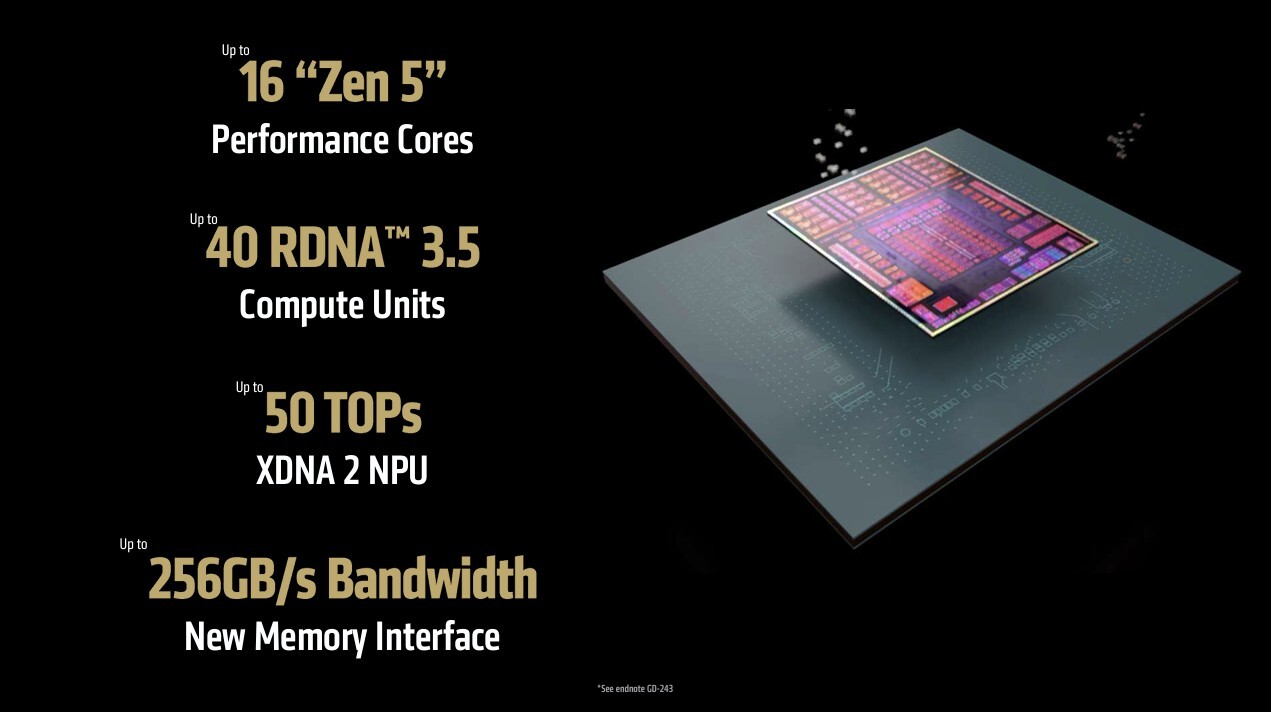
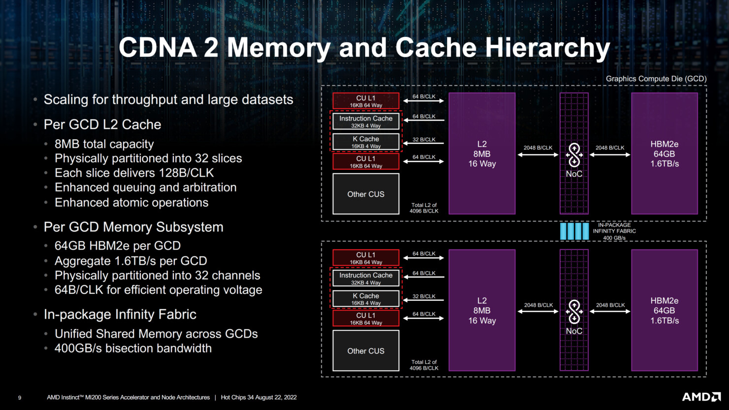
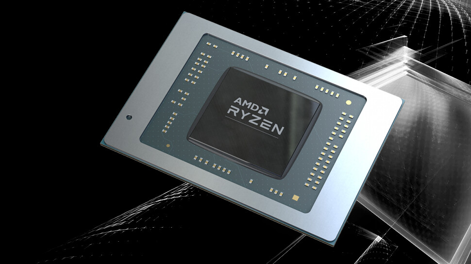
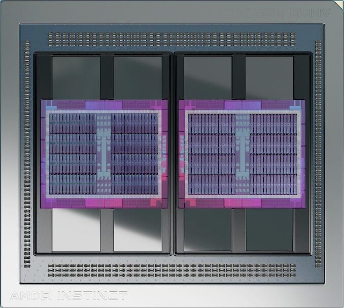
The "Strix Halo" processor is "Fire Range" on steroids. There are one or two "Zen 5" CCDs, for up to a 16-core/32-thread core configuration. Each of these "Zen 5" cores are unlike the ones on "Strix Point," in that they feature a fully unlocked AVX512 hardware pipeline (512-bit FP). The CCD shares a lavish 32 MB of L3 cache among 8 "Zen 5" cores. This is hardly the star attraction. Unlike "Fire Range," which features the small 6 nm client I/O die from "Granite Ridge," The new "Strix Halo" features a massive SoC die built on the 5 nm EUV foundry node. This packs the star attraction of the processor, it's oversized iGPU that has a massive 40 compute units (2,560 stream processors).


The "Strix Halo" processor is "Fire Range" on steroids. There are one or two "Zen 5" CCDs, for up to a 16-core/32-thread core configuration. Each of these "Zen 5" cores are unlike the ones on "Strix Point," in that they feature a fully unlocked AVX512 hardware pipeline (512-bit FP). The CCD shares a lavish 32 MB of L3 cache among 8 "Zen 5" cores. This is hardly the star attraction. Unlike "Fire Range," which features the small 6 nm client I/O die from "Granite Ridge," The new "Strix Halo" features a massive SoC die built on the 5 nm EUV foundry node. This packs the star attraction of the processor, it's oversized iGPU that has a massive 40 compute units (2,560 stream processors).