News Posts matching #Infinity Fabric

Return to Keyword Browsing

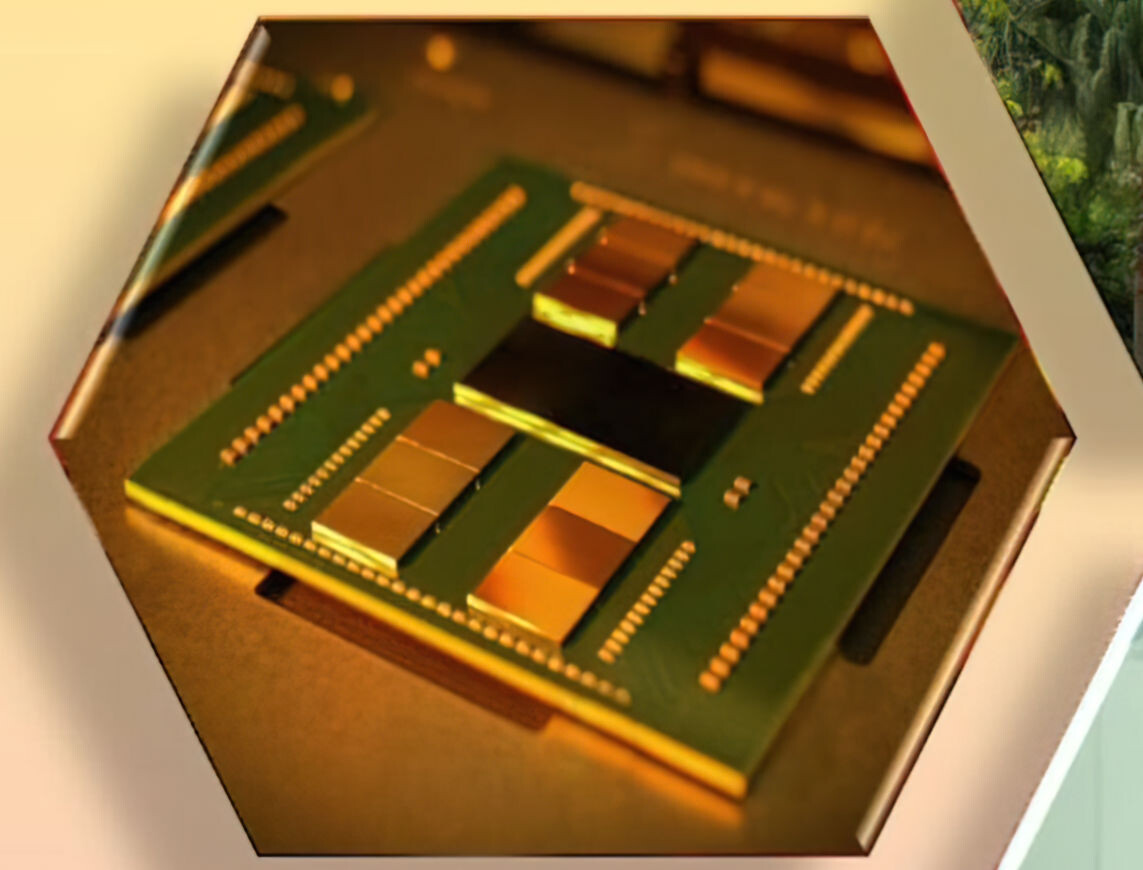
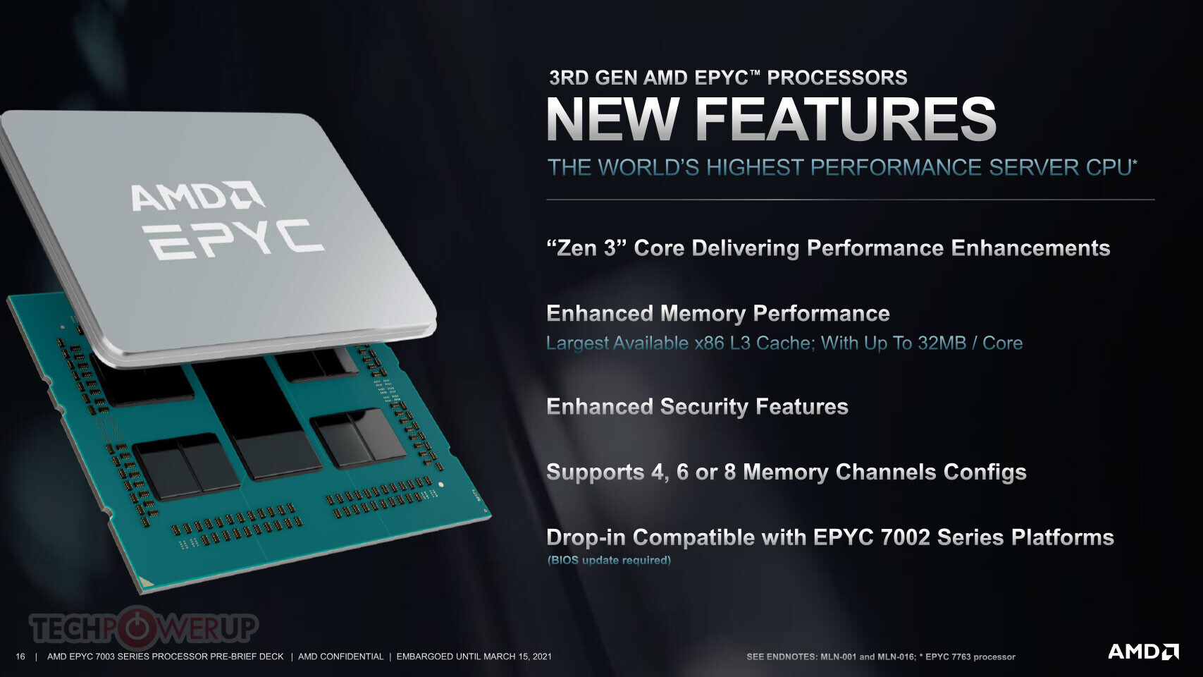
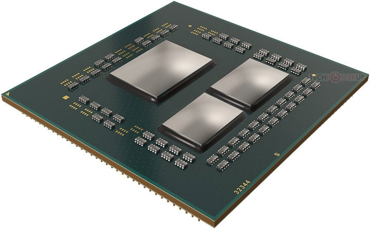
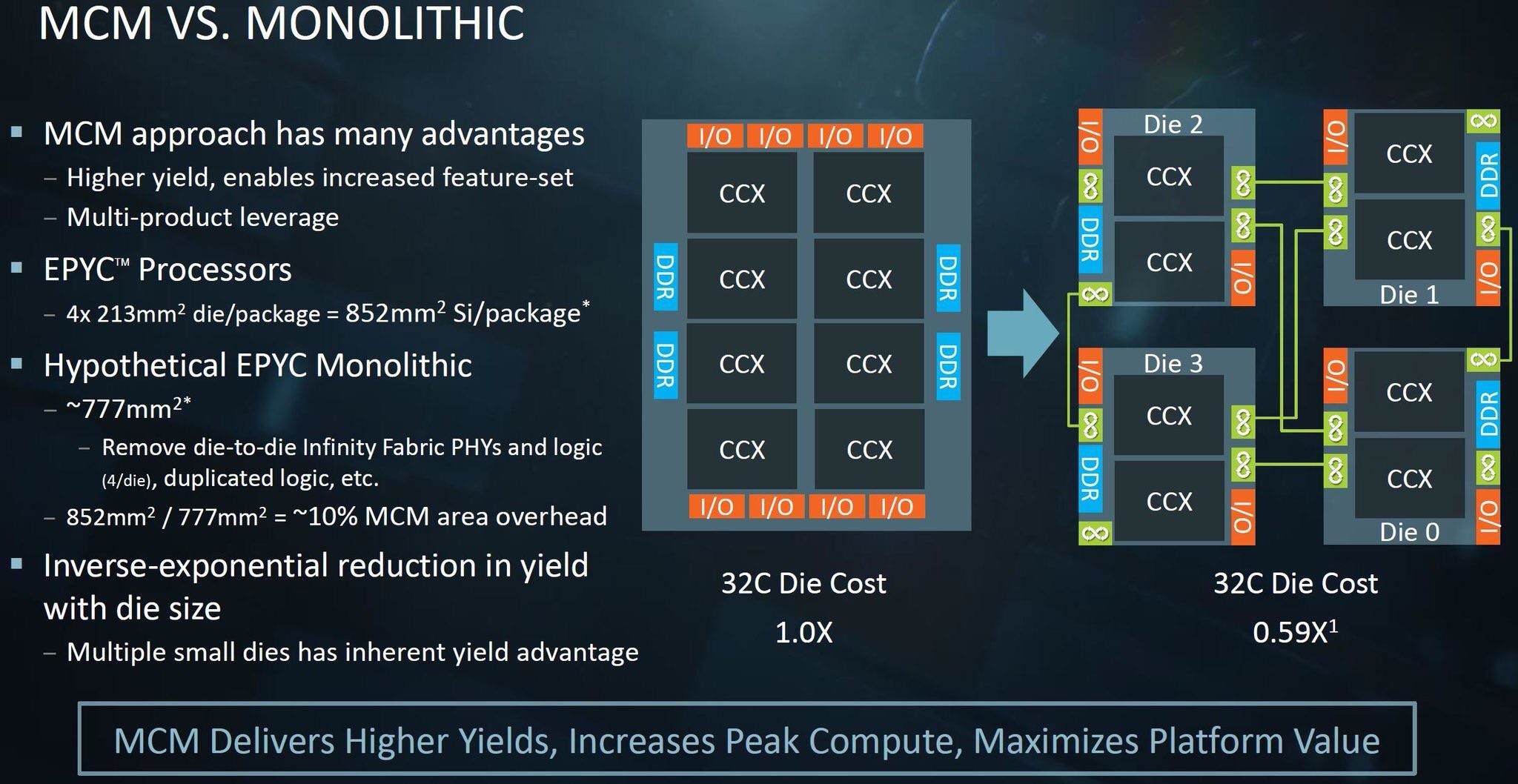
AMD EPYC "Genoa" Zen 4 Processor Multi-Chip Module Pictured

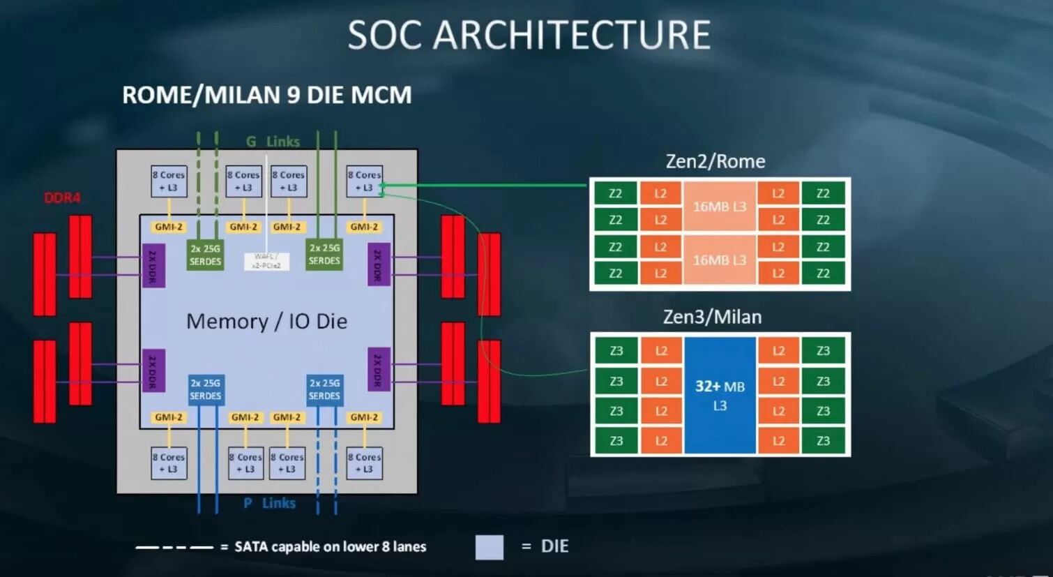
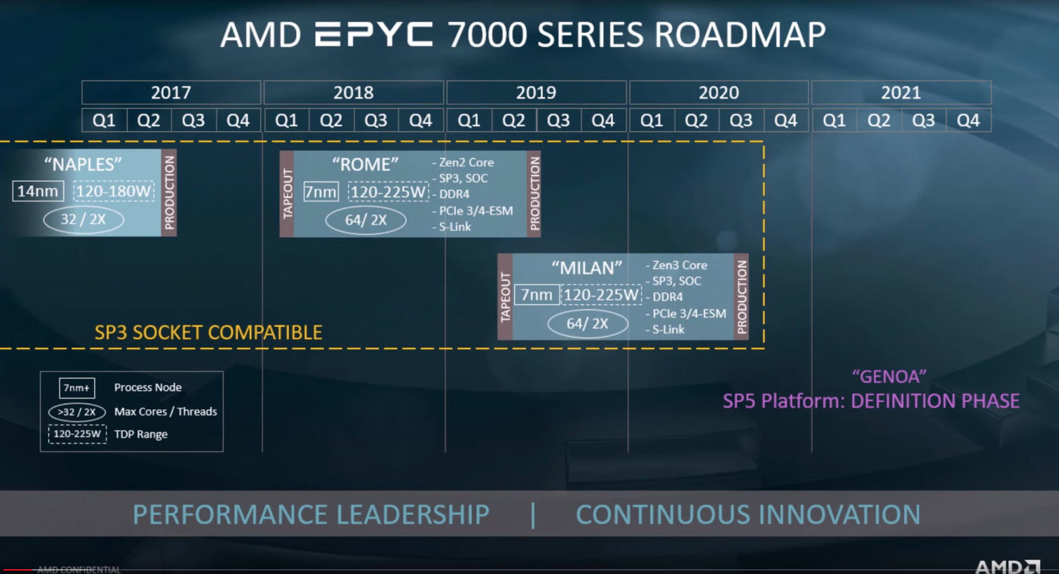
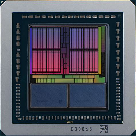
Here is the first picture of a next-generation AMD EPYC "Genoa" processor with its integrated heatspreader (IHS) removed. This is also possibly the first picture of a "Zen 4" CPU Complex Die (CCD). The picture reveals as many as twelve CCDs, and a large sIOD silicon. The "Zen 4" CCDs, built on the TSMC N5 (5 nm EUV) process, look visibly similar in size to the "Zen 3" CCDs built on the N7 (7 nm) process, which means the CCD's transistor count could be significantly higher, given the transistor-density gained from the 5 nm node. Besides more number-crunching machinery on the CPU core, we're hearing that AMD will increase cache sizes, particularly the dedicated L2 cache size, which is expected to be 1 MB per core, doubling from the previous generations of the "Zen" microarchitecture.

Each "Zen 4" CCD is reported to be about 8 mm² smaller in die-area than the "Zen 3" CCD, or about 10% smaller. What's interesting, though, is that the sIOD (server I/O die) is smaller in size, too, estimated to measure 397 mm², compared to the 416 mm² of the "Rome" and "Milan" sIOD. This is good reason to believe that AMD has switched over to a newer foundry process, such as the TSMC N7 (7 nm), to build the sIOD. The current-gen sIOD is built on Global Foundries 12LPP (12 nm). Supporting this theory is the fact that the "Genoa" sIOD has a 50% wider memory I/O (12-channel DDR5), 50% more IFOP ports (Infinity Fabric over package) to interconnect with the CCDs, and the mere fact that PCI-Express 5.0 and DDR5 switching fabric and SerDes (serializer/deserializers), may have higher TDP; which together compel AMD to use a smaller node such as 7 nm, for the sIOD. AMD is expected to debut the EPYC "Genoa" enterprise processors in the second half of 2022.

AMD's Robert Hallock Confirms Lack of Manual CPU Overclocking for Ryzen 7 5800X3D

In a livestream talking about AMD's mobile CPUs with HotHardware, Robert Hallock shone some light on the rumours about the Ryzen 7 5800X3D lacking manual overclocking. As per earlier rumours, something TechPowerUp! confirmed with our own sources, AMD's Ryzen 7 5800X3D lacks support for manual CPU overclocking and AMD asked its motherboard partners to remove these features in the UEFI. According to the livestream, these CPUs are said to be hard locked, so there's no workaround when it comes to adjusting the CPU multiplier or Voltage, but at least AMD has a good reason for it.

It turns out that the 3D V-Cache is Voltage limited to a maximum of 1.3 to 1.35 Volts, which means that the regular boost Voltage of individual Ryzen CPU cores, which can hit 1.45 to 1.5 Volts, would be too high for the 3D V-Cache to handle. As such, AMD implemented the restrictions for this CPU. However, the Infinity Fabric and memory bus can still be manually overclocked. The lower Voltage boost also helps explain why the Ryzen 7 5800X3D has lower boost clocks, as it's possible that the higher Voltages are needed to hit the higher frequencies.

AMD Announces Ryzen 7 5800X3D, World's Fastest Gaming Processor

AMD today announced its Spring 2022 update for the company's Ryzen desktop processors, with as many as seven new processor models in the retail channel. The lineup is led by the Ryzen 7 5800X3D 8-core/16-thread processor, which AMD claims is the "world's fastest gaming processor." This processor introduces the 3D Vertical Cache (3DV Cache) to the consumer space.

64 MB of fast SRAM is stacked on top of the region of the CCD (8-core chiplet) that has 32 MB of on-die L3 cache, with structural silicon leveling the region over the CPU cores with it. This SRAM is tied directly with the bi-directional ring-bus that interconnects the CPU cores, L3 cache, and IFOP (Infinity Fabric Over Package) interconnect. The result is 96 MB of seamless L3 cache, with each of the 8 "Zen 3" CPU cores having equal access to all of it.

AMD Details Instinct MI200 Series Compute Accelerator Lineup

AMD today announced the new AMD Instinct MI200 series accelerators, the first exascale-class GPU accelerators. AMD Instinct MI200 series accelerators includes the world's fastest high performance computing (HPC) and artificial intelligence (AI) accelerator,1 the AMD Instinct MI250X.

Built on AMD CDNA 2 architecture, AMD Instinct MI200 series accelerators deliver leading application performance for a broad set of HPC workloads. The AMD Instinct MI250X accelerator provides up to 4.9X better performance than competitive accelerators for double precision (FP64) HPC applications and surpasses 380 teraflops of peak theoretical half-precision (FP16) for AI workloads to enable disruptive approaches in further accelerating data-driven research.

AMD Instinct MI200: Dual-GPU Chiplet; CDNA2 Architecture; 128 GB HBM2E

AMD today announced the debut of its 6 nm CDNA2 (Compute-DNA) architecture in the form of the MI200 family. The new, dual-GPU chiplet accelerator aims to lead AMD into a new era of High Performance Computing (HPC) applications, the high margin territory it needs to compete in for continued, sustainable growth. To that end, AMD has further improved on a matured, compute-oriented architecture born with Graphics Core Next (GCN) - and managed to improve performance while reducing total die size compared to its MI100 family.

New AMD Radeon PRO W6000X Series GPUs Bring Groundbreaking High-Performance AMD RDNA 2 Architecture to Mac Pro

AMD today announced availability of the new AMD Radeon PRO W6000X series GPUs for Mac Pro. The new GPU product line delivers exceptional performance and incredible visual fidelity to power a wide variety of demanding professional applications and workloads, including 3D rendering, 8K video compositing, color correction and more.

Built on groundbreaking AMD RDNA 2 architecture, AMD Infinity Cache and other advanced technologies, the new workstation graphics line-up includes the AMD Radeon PRO W6900X and AMD Radeon PRO W6800X GPUs. Mac Pro users also have the option of choosing the AMD Radeon PRO W6800X Duo graphics card, a dual-GPU configuration that leverages high-speed AMD Infinity Fabric interconnect technology to deliver outstanding levels of compute performance.

AMD Announces 3rd Generation EPYC 7003 Enterprise Processors

AMD today announced its 3rd generation EPYC (7003 series) enterprise processors, codenamed "Milan." These processors combine up to 64 of the company's latest "Zen 3" CPU cores, with an updated I/O controller die, and promise significant performance uplifts and new security capabilities over the previous generation EPYC 7002 "Rome." The "Zen 3" CPU cores, AMD claims, introduce an IPC uplift of up to 19% over the previous generation, which when combined by generational increases in CPU clock speeds, bring about significant single-threaded performance increases. The processor also comes with large multi-threaded performance gains thanks to a redesigned CCD.

The new "Zen 3" CPU complex die (CCD) comes with a radical redesign in the arrangement of CPU cores, putting all eight CPU cores of the CCD in a single CCX, sharing a large 32 MB L3 cache. This the total amount of L3 cache addressable by a CPU core, and significantly reduces latencies for multi-threaded workloads. The "Milan" multi-chip module has up to eight such CCDs talking to a centralized server I/O controller die (sIOD) over the Infinity Fabric interconnect.

AMD Ryzen 5000 Series Features Three Synchronized Memory Clock Domains

A leaked presentation slide by AMD for its Ryzen 5000 series "Zen 3" processors reveals details of the processor's memory interface. Much like the Ryzen 3000 series "Matisse," the Ryzen 5000 series "Vermeer" is a multi-chip module of up to 16 CPU cores spread across two 8-core CPU dies, and a unified I/O die that handles the processor's memory-, PCIe, and SoC interfaces. There are three configurable clock domains that ensure the CPU cores are fed with data at the right speed, and to ensure that the MCM design doesn't pose bottlenecks to the memory performance.

The first domain is fclk or Infinity Fabric clock. Each of the two CCDs (8-core CPU dies) has just one CCX (CPU core complex) with 8 cores, and hence the CCD's internal Infinity Fabric cedes relevance to the IFOP (Infinity Fabric over Package) interconnect that binds the two CCDs and the cIOD (client I/O controller die) together. The next frequency is uclk, or the internal frequency of the dual-channel DDR4 memory controller contained in the cIOD. And lastly, the mclk, or memory clock is the industry-standard DRAM frequency.

AMD 4th Gen Ryzen "Vermeer" Zen 3 Rumored to Include 10-core Parts

Yuri "1usmus" Bubliy, author of DRAM Calculator for Ryzen and the upcoming ClockTuner for Ryzen, revealed three pieces of juicy details on the upcoming 4th Gen AMD Ryzen "Vermeer" performance desktop processors. He predicts AMD turning up CPU core counts with this generation, including the introduction of new 10-core SKUs, possibly to one-up Intel in the multi-threaded performance front. Last we heard, AMD's upcoming "Zen 3" CCDs (chiplets) feature 8 CPU cores sharing a monolithic 32 MB slab of L3 cache. This should, in theory, allow AMD to create 10-core chips with two CCDs, each with 5 cores enabled.

Next up, are two features that should interest overclockers - which is Bubliy's main domain. The processors should support a feature called "Curve Optimizer," enabling finer-grained control over the boost algorithm, and on a per-core basis. As we understand, the "curve" in question could even be voltage/frequency. It remains to be seen of the feature is leveraged at a CBS level (UEFI setup program), or by Ryzen Master. Lastly, there's mention of new Infinity Fabric dividers that apparently helps you raise DCT (memory controller) frequencies "slightly higher" in mixed mode. AMD is expected to debut its 4th Gen Ryzen "Vermeer" desktop processors within 2020.

AMD Confirms CDNA-Based Radeon Instinct MI100 Coming to HPC Workloads in 2H2020

Mark Papermaster, chief technology officer and executive vice president of Technology and Engineering at AMD, today confirmed that CDNA is on-track for release in 2H2020 for HPC computing. The confirmation was (adequately) given during Dell's EMC High-Performance Computing Online event. This confirms that AMD is looking at a busy 2nd half of the year, with both Zen 3, RDNA 2 and CDNA product lines being pushed to market.

CDNA is AMD's next push into the highly-lucrative HPC market, and will see the company differentiating their GPU architectures through market-based product differentiation. CDNA will see raster graphics hardware, display and multimedia engines, and other associated components being removed from the chip design in a bid to recoup die area for both increased processing units as well as fixed-function tensor compute hardware. CNDA-based Radeon Instinct MI100 will be fabricated under TSMC's 7 nm node, and will be the first AMD architecture featuring shared memory pools between CPUs and GPUs via the 2nd gen Infinity Fabric, which should bring about both throughput and power consumption improvements to the platform.

AMD Announces Radeon Pro VII Graphics Card, Brings Back Multi-GPU Bridge

AMD today announced its Radeon Pro VII professional graphics card targeting 3D artists, engineering professionals, broadcast media professionals, and HPC researchers. The card is based on AMD's "Vega 20" multi-chip module that incorporates a 7 nm (TSMC N7) GPU die, along with a 4096-bit wide HBM2 memory interface, and four memory stacks adding up to 16 GB of video memory. The GPU die is configured with 3,840 stream processors across 60 compute units, 240 TMUs, and 64 ROPs. The card is built in a workstation-optimized add-on card form-factor (rear-facing power connectors and lateral-blower cooling solution).

What separates the Radeon Pro VII from last year's Radeon VII is full double precision floating point support, which is 1:2 FP32 throughput compared to the Radeon VII, which is locked to 1:4 FP32. Specifically, the Radeon Pro VII offers 6.55 TFLOPs double-precision floating point performance (vs. 3.36 TFLOPs on the Radeon VII). Another major difference is the physical Infinity Fabric bridge interface, which lets you pair up to two of these cards in a multi-GPU setup to double the memory capacity, to 32 GB. Each GPU has two Infinity Fabric links, running at 1333 MHz, with a per-direction bandwidth of 42 GB/s. This brings the total bidirectional bandwidth to a whopping 168 GB/s—more than twice the PCIe 4.0 x16 limit of 64 GB/s.

AMD Announces the CDNA and CDNA2 Compute GPU Architectures

AMD at its 2020 Financial Analyst Day event unveiled its upcoming CDNA GPU-based compute accelerator architecture. CDNA will complement the company's graphics-oriented RDNA architecture. While RDNA powers the company's Radeon Pro and Radeon RX client- and enterprise graphics products, CDNA will power compute accelerators such as Radeon Instinct, etc. AMD is having to fork its graphics IP to RDNA and CDNA due to what it described as market-based product differentiation.

Data centers and HPCs using Radeon Instinct accelerators have no use for the GPU's actual graphics rendering capabilities. And so, at a silicon level, AMD is removing the raster graphics hardware, the display and multimedia engines, and other associated components that otherwise take up significant amounts of die area. In their place, AMD is adding fixed-function tensor compute hardware, similar to the tensor cores on certain NVIDIA GPUs.
AMD Datacenter GPU Roadmap CDNA CDNA2 AMD CDNA Architecture AMD Exascale Supercomputer

AMD Financial Analyst Day 2020 Live Blog

AMD Financial Analyst Day presents an opportunity for AMD to talk straight with the finance industry about the company's current financial health, and a taste of what's to come. Guidance and product teasers made during this time are usually very accurate due to the nature of the audience. In this live blog, we will post information from the Financial Analyst Day 2020 as it unfolds.
20:59 UTC: The event has started as of 1 PM PST. CEO Dr Lisa Su takes stage.

AMD Scores Another EPYC Win in Exascale Computing With DOE's "El Capitan" Two-Exaflop Supercomputer

AMD has been on a roll in both consumer, professional, and exascale computing environments, and it has just snagged itself another hugely important contract. The US Department of Energy (DOE) has just announced the winners for their next-gen, exascale supercomputer that aims to be the world's fastest. Dubbed "El Capitan", the new supercomputer will be powered by AMD's next-gen EPYC Genoa processors (Zen 4 architecture) and Radeon GPUs. This is the first such exascale contract where AMD is the sole purveyor of both CPUs and GPUs, with AMD's other design win with EPYC in the Cray Shasta being paired with NVIDIA graphics cards.

El Capitan will be a $600 million investment to be deployed in late 2022 and operational in 2023. Undoubtedly, next-gen proposals from AMD, Intel and NVIDIA were presented, with AMD winning the shootout in a big way. While initially the DOE projected El Capitan to provide some 1.5 exaflops of computing power, it has now revised their performance goals to a pure 2 exaflop machine. El Capitan willl thus be ten times faster than the current leader of the supercomputing world, Summit.

AMD Zen 3 Could Bid the CCX Farewell, Feature Updated SMT

With its next-generation "Zen 3" CPU microarchitecture designed for the 7 nm EUV silicon fabrication process, AMD could bid the "Zen" compute complex or CCX farewell, heralding chiplets with monolithic last-level caches (L3 caches) that are shared across all cores on the chiplet. AMD embraced a quad-core compute complex approach to building multi-core processors with "Zen." At the time, the 8-core "Zeppelin" die featured two CCX with four cores, each. With "Zen 2," AMD reduced the CPU chiplet to only containing CPU cores, L3 cache, and an Infinity Fabric interface, talking to an I/O controller die elsewhere on the processor package. This reduces the economic or technical utility in retaining the CCX topology, which limits the amount of L3 cache individual cores can access.

This and more juicy details about "Zen 3" were put out by a leaked (later deleted) technical presentation by company CTO Mark Papermaster. On the EPYC side of things, AMD's design efforts will be spearheaded by the "Milan" multi-chip module, featuring up to 64 cores spread across eight 8-core chiplets. Papermaster talked about how the individual chiplets will feature "unified" 32 MB of last-level cache, which means a deprecation of the CCX topology. He also detailed an updated SMT implementation that doubles the number of logical processors per physical core. The I/O interface of "Milan" will retain PCI-Express gen 4.0 and eight-channel DDR4 memory interface.

AMD Zen 2 EPYC "Rome" Launch Event Live Blog

AMD invited TechPowerUp to their launch event and editor's day coverage of Zen 2 EPYC processors based on the 7 nm process. The event was a day-long affair which included product demos and tours, and capped off with an official launch presentation which we are able to share with you live as the event goes on. Zen 2 with the Ryzen 3000-series processors ushered in a lot of excitement, and for good reason too as our own reviews show, but questions remained on how the platform would scale to the other end of the market. We already knew, for example, that AMD secured many contracts based on their first-generation EPYC processors, and no doubt the IPC increase and expected increased core count would cause similar, if not higher, interest here. We also expect to know shortly about the various SKUs and pricing involved, and also if AMD wants to shed more light on the future of the Threadripper processor family. Read below, and continue past the break, for our live coverage.
21:00 UTC: Lisa Su is on the stage at the Palace of Fine Arts events venue in San Francisco to present AMD's latest developments on EPYC for datacenters, using the Zen 2 microarchitecture.

21:10 UTC: AMD focuses not just on delivering a single chip, but it's goal is to deliver a complete solution for the enterprise.

AMD Reports Second Quarter 2019 Financial Results

AMD (NASDAQ:AMD) today announced revenue for the second quarter of 2019 of $1.53 billion, operating income of $59 million, net income of $35 million and diluted earnings per share of $0.03. On a non-GAAP basis, operating income was $111 million, net income was $92 million and diluted earnings per share was $0.08.

"I am pleased with our financial performance and execution in the quarter as we ramped production of three leadership 7nm product families," said Dr. Lisa Su, AMD president and CEO. "We have reached a significant inflection point for the company as our new Ryzen, Radeon and EPYC processors form the most competitive product portfolio in our history and are well positioned to drive significant growth in the second half of the year."

AMD Zen 2 CPUs to Support Official JEDEC 3200 MHz Memory Speeds

An AMD-based system's most important performance pairing lies in the CPU and system RAM, as a million articles written ever since the introduction of AMD's first generation Ryzen CPUs have shown (remember the races for Samsung B-die based memory?). There are even tools that allow you to eke out the most performance out of your AMD system via fine memory overclocking and timings adjustment, which just goes to show the importance the enthusiast community derives from such tiny details that maximize your AMD Zen-based CPU performance. Now, notorious leaker @momomo_us has seemingly confirmed that AMD has worked wonders on its memory controller, achieving a base JEDEC 3200 MHz specification - up from the previously officially supported DDR4-2666 speeds in the first-gen Ryzen (updated to DDR4-2933 speeds on the 12 nm update).

AMD Ryzen 3000 "Zen 2" a Memory OC Beast, DDR4-5000 Possible

AMD's 3rd generation Ryzen (3000-series) processors will overcome a vast number of memory limitations faced by older Ryzen chips. With Zen 2, the company decided to separate the memory controller from the CPU cores into a separate chip, called "IO die". Our resident Ryzen memory guru Yuri "1usmus" Bubliy, author of DRAM Calculator for Ryzen, found technical info that confirms just how much progress AMD has been making.

The third generation Ryzen processors will be able to match their Intel counterparts when it comes to memory overclocking. In the Zen 2 BIOS, the memory frequency options go all the way up to "DDR4-5000", which is a huge increase over the first Ryzens. The DRAM clock is still linked to the Infinity Fabric (IF) clock domain, which means at DDR4-5000, Infinity Fabric would tick at 5000 MHz DDR, too. Since that rate is out of reach for IF, AMD has decided to add a new 1/2 divider mode for their on-chip bus. When enabled, it will run Infinity Fabric at half the DRAM actual clock (eg: 1250 MHz for DDR4-5000).

AMD Ryzen 3000 "Zen 2" BIOS Analysis Reveals New Options for Overclocking & Tweaking

AMD will launch its 3rd generation Ryzen 3000 Socket AM4 desktop processors in 2019, with a product unveiling expected mid-year, likely on the sidelines of Computex 2019. AMD is keeping its promise of making these chips backwards compatible with existing Socket AM4 motherboards. To that effect, motherboard vendors such as ASUS and MSI began rolling out BIOS updates with AGESA-Combo 0.0.7.x microcode, which adds initial support for the platform to run and validate engineering samples of the upcoming "Zen 2" chips.

At CES 2019, AMD unveiled more technical details and a prototype of a 3rd generation Ryzen socket AM4 processor. The company confirmed that it will implement a multi-chip module (MCM) design even for their mainstream-desktop processor, in which it will use one or two 7 nm "Zen 2" CPU core chiplets, which talk to a 14 nm I/O controller die over Infinity Fabric. The two biggest components of the IO die are the PCI-Express root complex, and the all-important dual-channel DDR4 memory controller. We bring you never before reported details of this memory controller.

AMD Unveils World's First 7 nm GPUs - Radeon Instinct MI60, Instinct MI50

AMD today announced the AMD Radeon Instinct MI60 and MI50 accelerators, the world's first 7nm datacenter GPUs, designed to deliver the compute performance required for next-generation deep learning, HPC, cloud computing and rendering applications. Researchers, scientists and developers will use AMD Radeon Instinct accelerators to solve tough and interesting challenges, including large-scale simulations, climate change, computational biology, disease prevention and more.

"Legacy GPU architectures limit IT managers from effectively addressing the constantly evolving demands of processing and analyzing huge datasets for modern cloud datacenter workloads," said David Wang, senior vice president of engineering, Radeon Technologies Group at AMD. "Combining world-class performance and a flexible architecture with a robust software platform and the industry's leading-edge ROCm open software ecosystem, the new AMD Radeon Instinct accelerators provide the critical components needed to solve the most difficult cloud computing challenges today and into the future."

AMD Introduces Dynamic Local Mode for Threadripper: up to 47% Performance Gain

AMD has made a blog post describing an upcoming feature for their Threadripper processors called "Dynamic Local Mode", which should help a lot with gaming performance on AMD's latest flagship CPUs.
Threadripper uses four dies in a multi-chip package, of which only two have a direct access path to the memory modules. The other two dies have to rely on Infinity Fabric for all their memory accesses, which comes with a significant latency hit. Many compute-heavy applications can run their workloads in the CPU cache, or require only very little memory access; these are not affected. Other applications, especially games, spread their workload over multiple cores, some of which end up with higher memory latency than expected, which results in a suboptimal performance.

AMD Implements xGMI for "Vega 20" as Competition to NVLink

xGMI (inter-chip global memory interconnect) is a cable-capable version of AMD's Infinity Fabric interconnect. A line of code in the latest version of AMDGPU Linux drivers reveals that "Vega 20" will support xGMI. This line tells the driver to check the state of xGMI link. A practical implementation of this could be inter-card high-bandwidth bridge connectivity that would otherwise saturate the PCI-Express host bus; similar to NVIDIA's usage of the new NVLink bridge for Quadro and Tesla products based on its "Volta" and "Turing" GPU architectures.

By no means should xGMI and NVLink implementations be interpreted as a coming back of multi-GPU to the gaming space. There are still no takers for DirectX 12 multi-GPU, and fewer AAA games support SLI or CrossFire. Even at higher resolutions/refresh-rates, existing SLI/CrossFire physical-layer standards have sufficient bandwidth for multi-GPU. The upcoming GeForce RTX 2000 graphics cards feature a new multi-GPU connector that's physically NVLink, but this is probably an attempt by NVIDIA to discard the legacy SLI bus and minimize redundant interfaces on its silicon. The TU102 and TU104 chips are implemented in the enterprise segment with the Quadro RTX family. The main application of xGMI/NVLink is to make multi-GPU hardware setups abstract to deep-learning software, so hardware can scale in the background with memory access spanning multiple GPUs. "Vega 20" will be launched in Radeon Pro and Radeon Instinct avatars late-2018.

AMD Announces 2nd Generation Ryzen Threadripper 2000, up to 32 Cores/64 Threads!

AMD announced its second-generation Ryzen Threadripper high-end desktop (HEDT) processor series, succeeding its lean and successful first-generation that disrupted much of Intel's Core X HEDT series, forcing Intel to open up new high-core-count (HCC) market segments beyond its traditional $1000 price-point. AMD's 16-core $999 1950X proved competitive with even Intel's 12-core and 14-core SKUs priced well above the $1200-mark; and now AMD looks to beat Intel at its game, with the introduction of new 24-core and 32-core SKUs at prices that are sure to spell trouble for Intel's Core X HCC lineup. The lineup is partially open to pre-orders, with two SKUs launching within August (including the 32-core one), and two others in October.

At the heart of AMD's second-generation Ryzen Threadripper is the new 12 nm "Pinnacle Ridge" die, which made its debut with the 2nd Generation Ryzen AM4 family. This die proved to introduce 3-5 percent IPC improvements in single-threaded tasks, and multi-threaded improvements with an improved Precision Boost II algorithm, which boosted frequencies of each of 8 cores on-die. The Threadripper is still a multi-chip module, with 2 to 4 of these dies, depending on the SKU. There are four of these - the 12-core/24-thread Threadripper 2920X, the 16-core/32-thread Threadripper 2950X; the 24-core/48-thread Threadripper 2970WX, and the flagship 32-core/64-thread Threadripper 2990WX.

On The Coming Chiplet Revolution and AMD's MCM Promise

With Moore's Law being pronounced as within its death throes, historic monolithic die designs are becoming increasingly expensive to manufacture. It's no secret that both AMD and NVIDIA have been exploring an MCM (Multi-Chip-Module) approach towards diverting from monolithic die designs over to a much more manageable, "chiplet" design. Essentially, AMD has achieved this in different ways with its Zen line of CPUs (two CPU modules of four cores each linked via the company's Infinity Fabric interconnect), and their own R9 and Vega graphics cards, which take another approach in packaging memory and the graphics processing die in the same silicon base - an interposer.
Return to Keyword Browsing
Jul 2nd, 2025 22:29 CDT change timezone

New Forum Posts

Popular Reviews

TPU on YouTube

Controversial News Posts