News Posts matching #Infinity Fabric

Return to Keyword Browsing

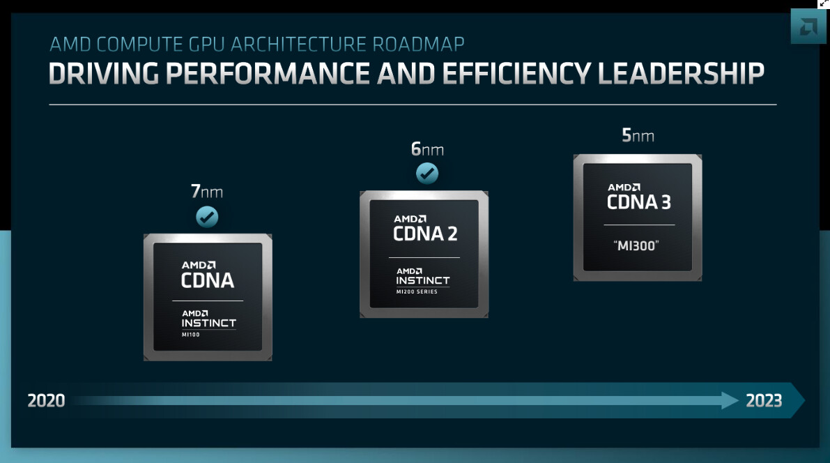
AMD Previews 432 GB HBM4 Instinct MI400 GPUs and Helios Rack‑Scale AI Solution

At its "Advancing AI 2025" event, AMD rolled out its new Instinct MI350 lineup on the CDNA 4 architecture and teased the upcoming UDNA-based AI accelerator. True to its roughly one‑year refresh rhythm, the company confirmed that the Instinct MI400 series will land in early 2026, showcasing a huge leap in memory, interconnect bandwidth, and raw compute power. Each MI400 card features twelve HBM4 stacks, providing a whopping 432 GB of on-package memory and pushing nearly 19.6 TB/s of memory bandwidth. Those early HBM4 modules deliver approximately 1.6 TB/s each, just shy of the 2 TB/s mark. On the compute front, AMD pegs the MI400 at 20 PetaFLOPS of FP8 throughput and 40 PetaFLOPS of FP4, doubling the sparse-matrix performance of today's MI355X cards. But the real game‑changer is how AMD is scaling those GPUs. Until now, you could connect up to eight cards via Infinity Fabric, and anything beyond that had to go over Ethernet.

The MI400's upgraded fabric link now offers 300 GB/s, nearly twice the speed of the MI350 series, allowing you to build full-rack clusters without relying on slower networks. That upgrade paves the way for "Helios," AMD's fully integrated AI rack solution. It combines upcoming EPYC "Venice" CPUs with MI400 GPUs and trim-to-fit networking gear, offering a turnkey setup for data center operators. AMD didn't shy away from comparisons, either. A Helios rack with 72 MI400 cards delivers approximately 3.1 ExaFLOPS of tensor performance and 31 TB of HBM4 memory. NVIDIA's Vera Rubin system, slated to feature 72 GPUs and 288 GB of memory each, is expected to achieve around 3.6 ExaFLOPS, with AMD's capabilities surpassing it in both bandwidth and capacity. And if that's not enough, whispers of a beefed‑up MI450X IF128 system are already swirling. Due in late 2026, it would directly link 128 GPUs with Infinity Fabric at 1.8 TB/s bidirectional per device, unlocking truly massive rack-scale AI clusters.

AMD Instinct MI350X Series AI GPU Silicon Detailed

AMD today unveiled its Instinct MI350X series AI GPU. Based on the company's latest CDNA 4 compute architecture, the MI350X is designed to compete with NVIDIA B200 "Blackwell" AI GPU series, with the top-spec Instinct MI355X being compared by AMD to the B200 in its presentation. The chip debuts not just the CDNA 4 architecture, but also the latest ROCm 7 software stack, and hardware ecosystem based on the industry-standard Open Compute Project specification, which combines AMD EPYC Zen 5 CPUs, Instinct MI350 series GPUs, AMD-Pensando Pollara scale-out NICs supporting Ultra-Ethernet, and industry-standard racks and nodes, both in air- and liquid-cooled form-factors.

The MI350 is a gigantic chiplet-based AI GPU that consists of stacked silicon. There are two base tiles called I/O dies (IODs), each built on the 6 nm TSMC N6 process. This tile has microscopic wiring for up to four Accelerator Compute Die (XCD) tiles stacked on top, besides the 128-channel HBM3E memory controllers, 256 MB of Infinity Cache memory, the Infinity Fabric interfaces, and a PCI-Express 5.0 x16 root complex. The XCDs are built on the 3 nm TSMC N3P foundry node. These contain a 4 MB L2 cache, and four shader engines, each with 9 compute units. Each XCD hence has 36 CU, and each IOD seats 144 CU. Two IODs are joined at the hip by a 5.5 TB/s bidirectional interconnect that enables full cache coherency among the two IODs. The package has a total of 288 CU. Each IOD controls four HBM3E stacks for 144 GB of memory, the package has 288 GB.

Compal Optimizes AI Workloads with AMD Instinct MI355X at AMD Advancing AI 2025 and International Supercomputing Conference 2025

As AI computing accelerates toward higher density and greater energy efficiency, Compal Electronics (Compal; Stock Ticker: 2324.TW), a global leader in IT and computing solutions, unveiled its latest high-performance server platform: SG720-2A/ OG720-2A at both AMD Advancing AI 2025 in the U.S. and the International Supercomputing Conference (ISC) 2025 in Europe. It features the AMD Instinct MI355X GPU architecture and offers both single-phase and two-phase liquid cooling configurations, showcasing Compal's leadership in thermal innovation and system integration. Tailored for next-generation generative AI and large language model (LLM) training, the SG720-2A/OG720-2A delivers exceptional flexibility and scalability for modern data center operations, drawing significant attention across the industry.

With generative AI and LLMs driving increasingly intensive compute demands, enterprises are placing greater emphasis on infrastructure that offers both performance and adaptability. The SG720-2A/OG720-2A emerges as a robust solution, combining high-density GPU integration and flexible liquid cooling options, positioning itself as an ideal platform for next-generation AI training and inference workloads.

AMD Prepares Instinct MI450X IF128 Rack‑Scale System with 128 GPUs

According to SemiAnalysis, AMD has planned its first-ever rack-scale GPU cluster for the second half of 2026, when it shows its first rack‑scale accelerator, the Instinct MI450X IF128. Built on what's expected to be a 3 nm‑class TSMC process and packaged with CoWoS‑L, each MI450X IF128 card will include at least 288 GB of HBM4 memory. That memory will sustain up to 18 TB/s of bandwidth, driving around 50 PetaFLOPS of FP4 compute while drawing between 1.6 and 2.0 kW of power. In our recent article, we outlined that AMD split the Instinct MI400 series into HPC-first MI430X and MI450X for AI. Now for AI-focused MI450X, the company created both an "IF64" backplane for simpler single‑rack installs and the full‑blown "IF128" for maximum density. The IF128 version links 128 GPUs over an Ethernet‑based Infinity Fabric network and uses UALink instead of PCIe to connect each GPU to three built‑in Pensando 800 GbE NICs. That design delivers about 1.8 TB/s of unidirectional bandwidth per GPU and a total of 2,304 TB/s across the rack.

With 128 GPUs each offering 50 PetaFLOPS of FP4 compute and 288 GB of HBM4 memory, the MI450X IF128 system delivers a combined 6,400 PetaFLOPS and 36.9 TB of high‑bandwidth memory, and MI450X IF64 provides about half of that. Since AI deployments require massive density of rack systems, AMD plans to possibly outnumber NVIDIA's upcoming system known as "Vera Rubin" VR200 NVL144 (144 compute dies, 72 GPUs), which tops out at 3,600 PetaFLOPS and 936 TB/s of memory bandwidth—about half of what AMD's IF128 approach promises. AMD will have a possibly more powerful system architecture than NVIDIA until the launch of VR300 "Ultra" NVL576, which has 144 GPUs, each carrying four compute dies, totaling 576 compute chiplets.

ASUS Introduces New "AI Cache Boost" BIOS Feature - R&D Team Claims Performance Uplift

Large language models (LLMs) love large quantities of memory—so much so, in fact, that AI enthusiasts are turning to multi-GPU setups to make even more VRAM available for their AI apps. But since many current LLMs are extremely large, even this approach has its limits. At times, the GPU will decide to make use of CPU processing power for this data, and when it does, the performance of your CPU cache and DRAM comes into play. All this means that when it comes to the performance of AI applications, it's not just the GPU that matters, but the entire pathway that connects the GPU to the CPU to the I/O die to the DRAM modules. It stands to reason, then, that there are opportunities to boost AI performance by optimizing these elements.

That's exactly what we've found as we've spent time in our R&D labs with the latest AMD Ryzen CPUs. AMD just launched two new Ryzen CPUs with AMD 3D V-Cache Technology, the AMD Ryzen 9 9950X3D and Ryzen 9 9900X3D, pushing the series into new performance territory. After testing a wide range of optimizations in a variety of workloads, we uncovered a range of settings that offer tangible benefits for AI enthusiasts. Now, we're ready to share these optimizations with you through a new BIOS feature: AI Cache Boost. Available through an ASUS AMD 800 Series motherboard and our most recent firmware update, AI Cache Boost can accelerate performance up to 12.75% when you're working with massive LLMs.

AMD Launches the EPYC Embedded 9005 "Turin" Family of Server Processors

AMD today launched the EPYC Embedded 9005 line of server processors in the embedded form-factor. These are non-socketed variants of the EPYC 9005 "Turin" server processors. The chips are intended for servers and other enterprise applications where processor replacements or upgradability are not a consideration. The EPYC Embedded 9005 "Turin" are otherwise every bit similar to the regular socketed EPYC 9005 series. These chips are based on a BGA version of the "Turin" chiplet-based processor, and powered by the "Zen 5" microarchitecture. Besides the BGA package, the EPYC Embedded 9005 series comes with a few features relevant to its form-factor and target use-cases.

To begin with, the EPYC Embedded 9005 "Turin" series comes with NTB (non-transparent bridging), a technology that enables high-performance data transfer between two processor packages across different memory domains. NTB doesn't use Infinity Fabric or even CXL, but a regular PCI-Express 5.0 x16 connection. It isn't intended to provide cache coherence, but to absorb faults across various memory domains. Next up, the series supports DRAM flush for enhanced power-loss mitigation. Upon detecting a power loss, the processor immediately dumps memory onto NVMe storage, before the machine turns off. On restart, the BIOS copies this memory dump from the NVMe SSD back to DRAM. Thirdly, the processors in the series support dual SPI flash interfaces, which enables system architects to embed lightweight operating systems directly onto a 64 MB SPI flash ROM, besides the primary SPI flash that stores the system BIOS. This lightweight OS can act like a bootloader for operating systems in other local storage devices.

AMD Zen 6 Powers "Medusa Point" Mobile and "Olympic Ridge" Desktop Processors

AMD is readying two important client segment processors powered by the next-generation "Zen 6" microarchitecture, according to a sensational new report by Moore's Law is Dead. These are the "Medusa Point" mobile processor, and the "Olympic Ridge" desktop. The former is a BGA roughly the size and Z-Height of the current "Strix Point," but the latter is being designed for the existing Socket AM5, making it the third (and probably final) microarchitecture to do so. If you recall, Socket AM4 served three generations of Zen, not counting the refreshed "Zen+." At the heart of the effort is a new CPU complex die (CCD) that AMD plans to use across its client and server lineup.

The "Zen 6" performance CCD is being designed for a 3 nm-class node, likely the TSMC N3E. This node promises a significant increase in transistor density, power, and clock speed improvements over the current TSMC N4P node being used to build the "Zen 5" CCD. Here's where it gets interesting. The CCD contains twelve full-sized "Zen 6" cores, marking the first increase in core-counts of AMD's performance cores since its very first "Zen" CCD. All 12 of these cores are part of a single CPU core complex (CCX), and share a common L3 cache. There could be a proportionate increase in cache size to 48 MB. AMD is also expected to improve the way the CCDs communicate with the I/O die and among each other.

AMD to Build Next-Gen I/O Dies on Samsung 4nm, Not TSMC N4P

Back in January, we covered a report about AMD designing its next-generation "Zen 6" CCDs on a 3 nm-class node by TSMC, and developing a new line of server and client I/O dies (cIOD and sIOD). The I/O die is a crucial piece of silicon that contains all the uncore components of the processor, including the memory controllers, the PCIe root complex, and Infinity Fabric interconnects to the CCDs and multi-socket connections. Back then it was reported that these new-generation I/O dies were being designed on the 4 nm silicon fabrication process, which was interpreted as being AMD's favorite 4 nm-class node, the TSMC N4P, on which the company builds everything from its current "Strix Point" mobile processors to the "Zen 5" CCDs. It turns out that AMD has other plans, and is exploring a 4 nm-class node by Samsung.

This node is very likely the Samsung 4LPP, also known as the SF4, which has been in mass-production since 2022. The table below shows how the SF4 compares with TSMC N4P and Intel 4, where it is shown striking a balance between the two. We have also added values for the TSMC N5 node from which the N4P is derived from, and you can see that the SF4 offers comparable transistor density to the N5, and is a significant improvement in transistor density over the TSMC N6, which AMD uses for its current generation of sIOD and cIOD. The new 4 nm node will allow AMD to reduce the TDP of the I/O die, implement a new power management solution, and more importantly, the need for a new I/O die is driven by the need for updated memory controllers that support higher DDR5 speeds and compatibility with new kinds of DIMMs, such as CUDIMMs, RDIMMs with RCDs, etc.

AMD Debuts Ryzen AI Max Series "Strix Halo" SoC: up to 16 "Zen 5" cores, Massive iGPU

AMD at the 2025 International CES debuted the Ryzen AI Max 300 series of mobile processors. These chips are designed to go up against the Apple M4 Pro, or the chip that powers the Apple MacBook Pro. The idea behind it is to provide leadership CPU and graphics performance from a single package, minimizing the PCB footprint from having a discrete GPU. In stark contrast, the Intel Core Ultra 200V "Lunar Lake," is designed more to go against the Apple M4, or the chips that power the latest MacBook Air but not quite the MacBook Pro. What sets "Strix Halo" functionally apart from "Lunar Lake" or even the M4 Pro, is that the AMD chip doesn't have memory-on-package (MoP), it relies on discrete LPDDR5X memory chips.

The "Strix Halo" processor is "Fire Range" on steroids. There are one or two "Zen 5" CCDs, for up to a 16-core/32-thread core configuration. Each of these "Zen 5" cores are unlike the ones on "Strix Point," in that they feature a fully unlocked AVX512 hardware pipeline (512-bit FP). The CCD shares a lavish 32 MB of L3 cache among 8 "Zen 5" cores. This is hardly the star attraction. Unlike "Fire Range," which features the small 6 nm client I/O die from "Granite Ridge," The new "Strix Halo" features a massive SoC die built on the 5 nm EUV foundry node. This packs the star attraction of the processor, it's oversized iGPU that has a massive 40 compute units (2,560 stream processors).

Social Media Imagines AMD "Navi 48" RDNA 4 to be a Dual-Chiplet GPU

A Chinese tech forum ChipHell user who goes by zcjzcj11111 sprung up a fascinating take on what the next-generation AMD "Navi 48" GPU could be, and put their imagination on a render. Apparently, the "Navi 48," which powers AMD's series-topping performance-segment graphics card, is a dual chiplet-based design, similar to the company's latest Instinct MI300 series AI GPUs. This won't be a disaggregated GPU such as the "Navi 31" and "Navi 32," but rather a scale-out multi-chip module of two GPU dies that can otherwise run on their own in single-die packages. You want to call this a multi-GPU-on-a-stick? Go ahead, but there are a couple of changes.

On AMD's Instinct AI GPUs, the chiplets have full cache coherence with each other, and can address memory controlled by each other. This cache coherence makes the chiplets work like one giant chip. In a multi-GPU-on-a-stick, there would be no cache coherence, the two dies would be mapped by the host machine as two separate devices, and then you'd be at the mercy of implicit or explicit multi-GPU technologies for performance to scale. This isn't what's happening on AI GPUs—despite multiple chiplets, the GPU is seen by the host as a single PCI device with all its cache and memory visible to software as a contiguously addressable block.

AMD Granite Ridge "Zen 5" Processor Annotated

High-resolution die-shots of the AMD "Zen 5" 8-core CCD were released and annotated by Nemez, Fitzchens Fitz, and HighYieldYT. These provide a detailed view of how the silicon and its various components appear, particularly the new "Zen 5" CPU core with its 512-bit FPU. The "Granite Ridge" package looks similar to "Raphael," with up to two 8-core CPU complex dies (CCDs) depending on the processor model, and a centrally located client I/O die (cIOD). This cIOD is carried over from "Raphael," which minimizes product development costs for AMD at least for the uncore portion of the processor. The "Zen 5" CCD is built on the TSMC N4P (4 nm) foundry node.

The "Granite Ridge" package sees the up to two "Zen 5" CCDs snuck up closer to each other than the "Zen 4" CCDs on "Raphael." In the picture above, you can see the pad of the absent CCD behind the solder mask of the fiberglass substrate, close to the present CCD. The CCD contains 8 full-sized "Zen 5" CPU cores, each with 1 MB of L2 cache, and a centrally located 32 MB L3 cache that's shared among all eight cores. The only other components are an SMU (system management unit), and the Infinity Fabric over Package (IFoP) PHYs, which connect the CCD to the cIOD.

AMD Strix Point Silicon Pictured and Annotated

The first die shot of AMD's new 4 nm "Strix Point" mobile processor surfaced, thanks to an enthusiast on Chinese social media. "Strix Point" is a significantly larger die than "Phoenix." It measures 12.06 mm x 18.71 mm (L x W), compared to the 9.06 mm x 15.01 mm of "Phoenix." Much of this die size increase comes from the larger CPU, iGPU, and NPU. The process has been improved from TSMC N4 on "Phoenix" and its derivative "Hawk Point," to the newer TSMC N4P node.

Nemez (GPUsAreMagic) annotated the die shot in great detail. The CPU now has 12 cores spread across two CCX, one of which contains four "Zen 5" cores sharing a 16 MB L3 cache; and the other with eight "Zen 5c" cores sharing an 8 MB L3 cache. The two CCXs connect to the rest of the chip over Infinity Fabric. The rather large iGPU takes up the central region of the die. It is based on the RDNA 3.5 graphics architecture, and features 8 workgroup processors (WGPs), or 16 compute units (CU) worth 1,024 stream processors. Other key components include four render backends worth 16 ROPs, and control logic. The GPU has its own 2 MB of L2 cache that cushions transfers to the Infinity Fabric.

AMD Strix Point SoC Reintroduces Dual-CCX CPU, Other Interesting Silicon Details Revealed

Since its reveal last week, we got a slightly more technical deep-dive from AMD on its two upcoming processors—the "Strix Point" silicon powering its Ryzen AI 300 series mobile processors; and the "Granite Ridge" chiplet MCM powering its Ryzen 9000 desktop processors. We present a closer look into the "Strix Point" SoC in this article. It turns out that "Strix Point" takes a significantly different approach to heterogeneous multicore than "Phoenix 2." AMD gave us a close look at how this works. AMD built the "Strix Point" monolithic silicon on the TSMC N4P foundry node, with a die-area of around 232 mm².

The "Strix Point" silicon sees the company's Infinity Fabric interconnect as its omnipresent ether. This is a point-to-point interconnect, unlike the ringbus on some Intel processors. The main compute machinery on the "Strix Point" SoC are its two CPU compute complexes (CCX), each with a 32b (read)/16b (write) per cycle data-path to the fabric. The concept of CCX makes a comeback with "Strix Point" after nearly two generations of "Zen." The first CCX contains the chip's four full-sized "Zen 5" CPU cores, which share a 16 MB L3 cache among themselves. The second CCX contains the chip's eight "Zen 5c" cores that share a smaller 8 MB L3 cache. Each of the 12 cores has a 1 MB dedicated L2 cache.

Ryzen 9000 Chip Layout: New Details Announced

AMD "Granite Ridge" is codename for the four new Ryzen 9000 series desktop processors the company plans to launch on July 31, 2024. The processor is built in the Socket AM5 package, and is meant to be backwards compatible with AMD 600-series chipset motherboards, besides the new 800-series chipset ones that will launch alongside. "Granite Ridge" is a chiplet-based processor, much like the Ryzen 7000 "Raphael," Ryzen 5000 "Vermeer," and Ryzen 3000 "Matisse." AMD is carrying over the 6 nm client I/O die over from "Raphael" in an effort to minimize development costs, much in the same way it carried over the 12 nm cIOD for "Vermeer" from "Matisse."

The SoC I/O features of "Granite Ridge" are contemporary, with its awesome 28-lane PCI-Express Gen 5 root complex that allows a PCI-Express 5.0 x16, two CPU-attached M.2 Gen 5 slots, and a Gen 5 x4 chipset bus. There's also a basic integrated graphics solution based on the older RDNA 2 graphics architecture; which should make these processors fit for all use-cases that don't need discrete graphics. The iGPU even has multimedia accelerators, an audio coprocessor, a display controller, and USB 3.2 interfaces from the processor.

ASRock Rack Unveils GPU Servers, Offers AI GPU Choices from All Three Brands

ASRock Rack sells the entire stack of servers a data-center could possibly want, and at Computex 2024, the company showed us their servers meant for AI GPUs. The 6U8M-GENOA2, as its name suggests, is a 6U server based on 2P AMD EPYC 9004 series "Genoa" processors in the SP5 package. You can configure it with even the variants of "Genoa" that come with 3D V-cache, for superior compute performance from the large cache. Each of the two SP5 sockets is wired to 12 DDR5 RDIMM slots, for a total of 24 memory channels. The server supports eight AMD Instinct MI300X or MI325X AI GPUs, which it wires out using Infinity Fabric links and PCIe Gen 5 x16 individually. A 3 kW 80 Plus Titanium PSU keeps the server fed. There are vacant Gen 5 x16 slots left even after connecting the GPUs, so you could give it a DPU-based 40 GbE NIC.

The 6U8X-EGS2 B100 is a 6U AI GPU server modeled along the 6U8M-GENOA2, with a couple of big changes. To begin with, the EPYC "Genoa" chips make way for a 2P Intel Xeon Socket E (LGA4677) CPU setup, for 2P Xeon 5 "Emerald Rapids" processors. Each socket is wired to 16 DDR5 DIMM slots (the processor itself has 8-channel DDR5, but this is a 2 DIMM-per-channel setup). The server integrates an NVIDIA NVSwitch that wires out NVLinks to eight NVIDIA B100 "Blackwell" AI GPUs. The server features eight HHHL PCIe Gen 5 x16, and five FHHL PCIe Gen 5 x16 connectors. There are vacant x16 slots for your DPU/NIC, you can even use an AIC NVIDIA BlueField card. The same 3 kW PSU as the "Genoa" system is also featured here.

Supermicro Extends AI and GPU Rack Scale Solutions with Support for AMD Instinct MI300 Series Accelerators

Supermicro, Inc., a Total IT Solution Manufacturer for AI, Cloud, Storage, and 5G/Edge, is announcing three new additions to its AMD-based H13 generation of GPU Servers, optimized to deliver leading-edge performance and efficiency, powered by the new AMD Instinct MI300 Series accelerators. Supermicro's powerful rack scale solutions with 8-GPU servers with the AMD Instinct MI300X OAM configuration are ideal for large model training.

The new 2U liquid-cooled and 4U air-cooled servers with the AMD Instinct MI300A Accelerated Processing Units (APUs) accelerators are available and improve data center efficiencies and power the fast-growing complex demands in AI, LLM, and HPC. The new systems contain quad APUs for scalable applications. Supermicro can deliver complete liquid-cooled racks for large-scale environments with up to 1,728 TFlops of FP64 performance per rack. Supermicro worldwide manufacturing facilities streamline the delivery of these new servers for AI and HPC convergence.

AMD Announces Appointment of New Corporate Fellows

AMD today announced the appointment of five technical leaders to the role of AMD Corporate Fellow. These appointments recognize each leader's significant impact on semiconductor innovation across various areas, from graphics architecture to advanced packaging. "David, Nathan, Suresh, Ben and Ralph - whose engineering contributions have already left an indelible mark on our industry - represent the best of our innovation culture," said Mark Papermaster, chief technology officer and executive vice president of Technology and Engineering at AMD. "Their appointments to Corporate Fellow will enable AMD to innovate in new dimensions as we work to deliver the most significant breakthroughs in high-performance computing in the decade ahead."

Appointment to AMD Corporate Fellow is an honor bestowed on the most accomplished AMD innovators. AMD Corporate Fellows are appointed after a rigorous review process that assesses not only specific technical contributions to the company, but also involvement in the industry, mentoring of others and improving the long-term strategic position of the company. Currently, only 13 engineers at AMD hold the title of Corporate Fellow.

AMD Explains the Economics Behind Chiplets for GPUs

AMD, in its technical presentation for the new Radeon RX 7900 series "Navi 31" GPU, gave us an elaborate explanation on why it had to take the chiplets route for high-end GPUs, devices that are far more complex than CPUs. The company also enlightened us on what sets chiplet-based packages apart from classic multi-chip modules (MCMs). An MCM is a package that consists of multiple independent devices sharing a fiberglass substrate.

An example of an MCM would be a mobile Intel Core processor, in which the CPU die and the PCH die share a substrate. Here, the CPU and the PCH are independent pieces of silicon that can otherwise exist on their own packages (as they do on the desktop platform), but have been paired together on a single substrate to minimize PCB footprint, which is precious on a mobile platform. A chiplet-based device is one where a substrate is made up of multiple dies that cannot otherwise independently exist on their own packages without an impact on inter-die bandwidth or latency. They are essentially what should have been components on a monolithic die, but disintegrated into separate dies built on different semiconductor foundry nodes, with a purely cost-driven motive.

AMD EPYC "Genoa" Zen 4 Product Stack Leaked

With its recent announcement of the Ryzen 7000 desktop processors, the action now shifts to the server, with AMD preparing a wide launch of its EPYC "Genoa" and "Bergamo" processors this year. Powered by the "Zen 4" microarchitecture, and contemporary I/O that includes PCI-Express Gen 5, CXL, and DDR5, these processors dial the CPU core-counts per socket up to 96 in case of "Genoa," and up to 128 in case of "Bergamo." The EPYC "Genoa" series represents the main trunk of the company's server processor lineup, with various internal configurations targeting specific use-cases.

The 96 cores are spread twelve 5 nm 8-core CCDs, each with a high-bandwidth Infinity Fabric path to the sIOD (server I/O die), which is very likely built on the 6 nm node. Lower core-count models can be built either by lowering the CCD count (ensuring more cores/CCD), or by reducing the number of cores/CCD and keeping the CCD-count constant, to yield more bandwidth/core. The leaked product-stack table below shows several of these sub-classes of "Genoa" and "Bergamo," classified by use-cases. The leaked slide also details the nomenclature AMD is using with its new processors. The leaked roadmap also mentions the upcoming "Genoa-X" processor for HPC and cloud-compute uses, which features the 3D Vertical Cache technology.

AMD Releases its CDNA2 MI250X "Aldebaran" HPC GPU Block Diagram

AMD in its HotChips 22 presentation released a block-diagram of its biggest AI-HPC processor, the Instinct MI250X. Based on the CDNA2 compute architecture, at the heart of the MI250X is the "Aldebaran" MCM (multi-chip module). This MCM contains two logic dies (GPU dies), and eight HBM2E stacks, four per GPU die. The two GPU dies are connected by a 400 GB/s Infinity Fabric link. They each have up to 500 GB/s of external Infinity Fabric bandwidth for inter-socket communications; and PCI-Express 4.0 x16 as the host system bus for AIC form-factors. The two GPU dies together make up 58 billion transistors, and are fabricated on the TSMC N6 (6 nm) node.

The component hierarchy of each GPU die sees eight Shader Engines share a last-level L2 cache. The eight Shader Engines total 112 Compute Units, or 14 CU per engine. The CDNA2 compute unit contains 64 stream processors making up the Shader Core, and four Matrix Core Units. These are specialized hardware for matrix/tensor math operations. There are hence 7,168 stream processors per GPU die, and 14,336 per package. AMD claims a 100% increase in double-precision compute performance over CDNA (MI100). AMD attributes this to increases in frequencies, efficient data paths, extensive operand reuse and forwarding; and power-optimization enabling those higher clocks. The MI200 is already powering the Frontier supercomputer, and is working for more design wins in the HPC space. The company also dropped a major hint that the MI300, based on CDNA3, will be an APU. It will incorporate GPU dies, core-logic, and CPU CCDs onto a single package, in what is a rival solution to NVIDIA Grace Hopper Superchip.

Ryzen 7000 Said to Have a DDR5-6000 Memory "Sweet Spot"

If you remember, there were quite a lot of discussions about memory speed "sweet spots" for both the Ryzen 3000- and Ryzen 5000-series, with the user experience not always meeting AMD's sweet spot for memory clocks. Now details of the Ryzen 7000-series memory sweet spot has arrived courtesy of Wccftech and the speed is said to be DDR5-6000. This is 400 MHz higher than the apparent official maximum memory clock speed of DDR5-5600, but as we know, the manufacturer's max memory clock is rarely the actual max. In AMD's case, things obviously work a bit differently, as the Infinity Fabric clock should ideally run at a 1:1 ratio with the memory in the case of the AM4 platform, to deliver best possible system performance and memory latencies.

That said, as we're using DDR memory, the actual clocks are only half of the memory speeds, so the IF clock is operating at no more than 2000 MHz if the memory is DDR4-4000. However, if the same applies to the Ryzen 7000-series, it appears that AMD has managed to bump the IF clocks by a not insignificant 1000 MHz, as the IF fabric would now be operating at up to 3000 MHz. This could see the Ryzen 7000-series offering better memory latencies than Intel's Alder Lake and upcoming Raptor Lake CPUs, as Intel is running DDR5 memory at a 2:1 ratio or a 4:1 ratio. AMD is said to still have a 2:1 ratio as well, but as with the AM4 CPUs, this offers worse overall performance.

Update 11:49 UTC: Yuri Bubliy aka @1usmus has confirmed on Twitter that the max IF frequency of 3000 MHz and it seems like AMD has added a range of new memory and bus related features to the AM5 platform, going by the additional features he posted.

AMD's Second Socket AM5 Ryzen Processor will be "Granite Ridge," Company Announces "Phoenix Point"

AMD in its 2022 Financial Analyst Day presentation announced the codename for the second generation of Ryzen desktop processors for Socket AM5, which is "Granite Ridge." A successor to the Ryzen 7000 "Raphael," the next-generation "Granite Ridge" processor will incorporate the "Zen 5" CPU microarchitecture, with its CPU complex dies (CCDs) built on the 4 nm silicon fabrication node. "Zen 5" will feature several core-level designs as detailed in our older article, including a redesigned front-end with greater parallelism, which should indicate a much large execution stage. The architecture could also incorporate AI/ML performance enhancements as AMD taps into Xilinx IP to add more fixed-function hardware backing the AI/ML capabilities of its processors.

The "Zen 5" microarchitecture makes its client debut with Ryzen "Granite Ridge," and server debut with EPYC "Turin." It's being speculated that AMD could give "Turin" a round of CPU core-count increases, while retaining the same SP5 infrastructure; which means we could see either smaller CCDs, or higher core-count per CCD with "Zen 5." Much like "Raphael," the next-gen "Granite Ridge" will be a series of high core-count desktop processors that will feature a functional iGPU that's good enough for desktop/productivity, though not gaming. AMD confirmed that it doesn't see "Raphael" as an APU, and that its definition of an "APU" is a processor with a large iGPU that's capable of gaming. The company's next such APU will be "Phoenix Point."

AMD CDNA3 Architecture Sees the Inevitable Fusion of Compute Units and x86 CPU at Massive Scale

AMD in its 2022 Financial Analyst Day presentation unveiled its next-generation CDNA3 compute architecture, which will see something we've been expecting for a while—a compute accelerator that has a large number of compute units for scalar processing, and a large number of x86-64 CPU cores based on some future "Zen" microarchitecture, onto a single package. The presence of CPU cores on the package would eliminate the need for the system to have an EPYC or Xeon processor at its head, and clusters of Instinct CDNA3 processors could run themselves without the need for a CPU and its system memory.

The Instinct CDNA3 processor will feature an advanced packaging technology that brings various IP blocks together as chiplets, each based on a node most economical to it, without compromising on its function. The package features stacked HBM memory, and this memory is shared not just by the compute units and x86 cores, but also forms part of large shared memory pools accessible across packages. 4th Generation Infinity Fabric ties it all together.

AMD Ryzen 7000 "Phoenix" APUs with RDNA3 Graphics to Rock Large 3D V-Cache

AMD's next-generation Ryzen 7000-series "Phoenix" mobile processors are all the rage these days. Bound for 2023, these chips feature a powerful iGPU based on the RDNA3 graphics architecture, with performance allegedly rivaling that of a GeForce RTX 3060 Laptop GPU—a popular performance-segment discrete GPU. What's more, AMD is also taking a swing at Intel in the CPU core-count game, by giving "Phoenix" a large number of "Zen 4" CPU cores. The secret ingredient pushing this combo, however, is a large cache.

AMD has used large caches to good effect both on its "Zen 3" processors, such as the Ryzen 7 5800X3D, where they're called 3D Vertical Cache (3D V-cache); as well as its Radeon RX 6000 discrete GPUs, where they're called Infinity Cache. The only known difference between the two is that the latter is fully on-die, while the former is stacked on top of existing silicon IP. It's being reported now, that "Phoenix" will indeed feature a stacked 3D V-cache.

"Navi 31" RDNA3 Sees AMD Double Down on Chiplets: As Many as 7

Way back in January 2021, we heard a spectacular rumor about "Navi 31," the next-generation big GPU by AMD, being the company's first logic-MCM GPU (a GPU with more than one logic die). The company has a legacy of MCM GPUs, but those have been a single logic die surrounded by memory stacks. The RDNA3 graphics architecture that the "Navi 31" is based on, sees AMD fragment the logic die into smaller chiplets, with the goal of ensuring that only those specific components that benefit from the TSMC N5 node (6 nm), such as the number crunching machinery, are built on the node, while ancillary components, such as memory controllers, display controllers, or even media accelerators, are confined to chiplets built on an older node, such as the TSMC N6 (6 nm). AMD had taken this approach with its EPYC and Ryzen processors, where the chiplets with the CPU cores got the better node, and the other logic components got an older one.

Greymon55 predicts an interesting division of labor on the "Navi 31" MCM. Apparently, the number-crunching machinery is spread across two GCD (Graphics Complex Dies?). These dies pack the Shader Engines with their RDNA3 compute units (CU), Command Processor, Geometry Processor, Asynchronous Compute Engines (ACEs), Rendering Backends, etc. These are things that can benefit from the advanced 5 nm node, enabling AMD to the CUs at higher engine clocks. There's also sound logic behind building a big GPU with two such GCDs instead of a single large GCD, as smaller GPUs can be made with a single such GCD (exactly why we have two 8-core chiplets making up a 16-core Ryzen processors, and the one of these being used to create 8-core and 6-core SKUs). The smaller GCD would result in better yields per wafer, and minimize the need for separate wafer orders for a larger die (such as in the case of the Navi 21).
Return to Keyword Browsing
Jul 6th, 2025 23:15 CDT change timezone

New Forum Posts

Popular Reviews

TPU on YouTube

Controversial News Posts