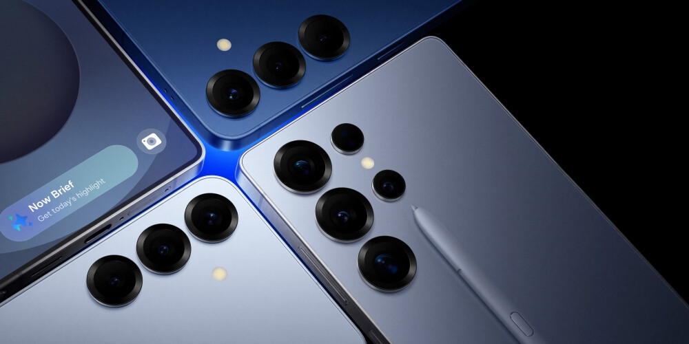
Samsung "Exynos 2500" Variant Tipped as SoC of Choice for "Galaxy Z Flip 7"
Yesterday, Chosun Daily published a news report that alleges a key "Galaxy Z Flip 7-related" decision made by Samsung leadership. According to smartphone industry moles, the oft-leaked/rumored "Exynos 2500" chipset destined to debut in the company's next-gen (horizontal) foldable smartphone design. As stated in the South Korean insider article: "this is the first time that Samsung's own mobile application processor (AP) is being installed in a foldable phone." Prior to 2025, Galaxy Flip Z product lines made use of Qualcomm Snapdragon chipsets. Throughout early 2025, leaks have linked the "troubled" Exynos 2500 mobile processor to futuristic Galaxy Z Flip 7, Fold 7, and affordable "FE" Enterprise Edition models. The emergence of a superior 2 nm "Exynos 2600" flagship chip—apparently tailored for Galaxy S26 devices (2026)—has allegedly relegated the lesser SoC into lower leagues.
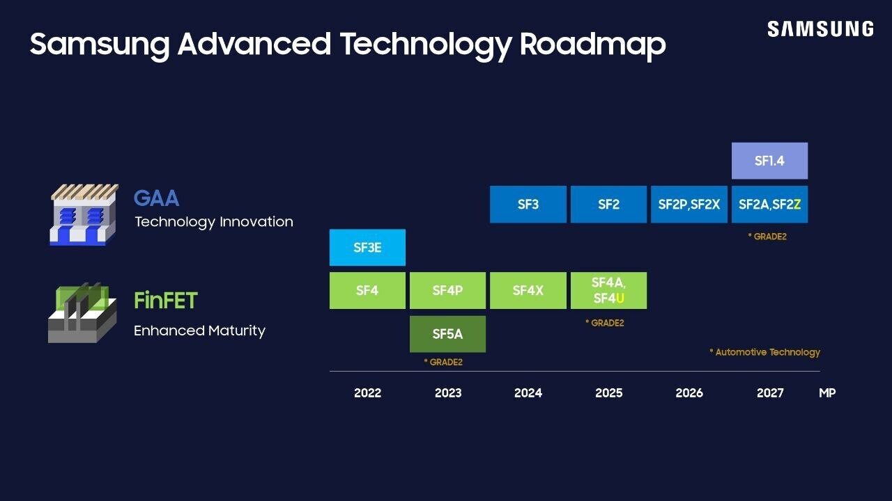
Semiconductor industry watchdogs reckon that the "Exynos 2500" will be manufactured via Samsung Foundry's own 3 nm GAA node process (aka SF3). Notebookcheck commented on this odd choice: "industry estimates from earlier suggested (SF3) yields were around 40%, making it less than ideal for mass production. But it seems Samsung decided to proceed anyway to save on costs, and likely give a new lease of life to its struggling foundry business." Jukanlosreve followed up with additional inside knowledge, just after the publication of Chosun Daily's news piece. The keen tracker of foundry-related revelations let slip with this observation: "the Exynos 2500 being used in the Flip 7 is said to be a lower-clocked chip due to its low yield. So it might as well be called the E2500E." Samsung is expected to unveil its Galaxy Z Flip 7 smartphone family during an "Unpacked" July event. Experts believe that Foundry employees will accumulate useful experience from the mass production of 3 nm parts; thus leading to improved output of finalized 2 nm (SF2) production lines.


Semiconductor industry watchdogs reckon that the "Exynos 2500" will be manufactured via Samsung Foundry's own 3 nm GAA node process (aka SF3). Notebookcheck commented on this odd choice: "industry estimates from earlier suggested (SF3) yields were around 40%, making it less than ideal for mass production. But it seems Samsung decided to proceed anyway to save on costs, and likely give a new lease of life to its struggling foundry business." Jukanlosreve followed up with additional inside knowledge, just after the publication of Chosun Daily's news piece. The keen tracker of foundry-related revelations let slip with this observation: "the Exynos 2500 being used in the Flip 7 is said to be a lower-clocked chip due to its low yield. So it might as well be called the E2500E." Samsung is expected to unveil its Galaxy Z Flip 7 smartphone family during an "Unpacked" July event. Experts believe that Foundry employees will accumulate useful experience from the mass production of 3 nm parts; thus leading to improved output of finalized 2 nm (SF2) production lines.