AMD Ryzen AI "Medusa Point" APU Could Arrive with Larger Footprint - BGA "FP10" Dimensions Leaked
Shipping manifests have served as fairly reliable sources of pre-launch information—Everest (aka Olrak29) has discovered many juicy details in recent times. Their latest sleuthing session—combing through NBD documents—has indicated AMD's (alleged) prepping of a larger socket design for next-generation mobile processors. A leaked document alludes to the existence of various "MEDUSA01" jig and block "FP10" socket validation parts. Current-generation Ryzen AI "Strix Point" 300 series APUs utilize the FP8 socket format. Based on the "MEDUSA01" shipping manifest, it seems that a successor will arrive with a larger footprint—measurements of 25 mm x 42.5 mm are repeated throughout the leaked description list. Industry watchdogs surmise that "Medusa Point's" BGA FP10 socket will be approximately 6% larger than its predecessor.
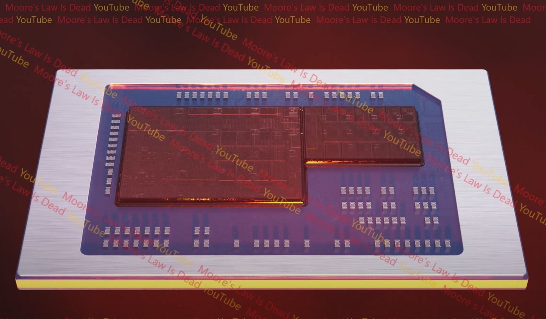
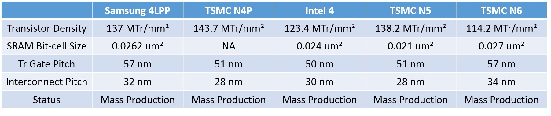
Mid-way through last month, insider theorizations pointed to "Medusa Point" being a chiplet-based design. A "single 12-core Zen 6 CCD" was linked to a TSMC 3 nm-class node, with "N4P" reportedly selected for a separate mobile client I/O die. Readily available 4 nm Ryzen AI "Strix Point" processors are monolithic in nature. Initial inside track info mentioned RDNA 4 technology in the same equation as "Medusa Point," but recent Team Red's recent-ish targeting of "GFX1153" places RDNA 3.5 as the de facto choice.

Mid-way through last month, insider theorizations pointed to "Medusa Point" being a chiplet-based design. A "single 12-core Zen 6 CCD" was linked to a TSMC 3 nm-class node, with "N4P" reportedly selected for a separate mobile client I/O die. Readily available 4 nm Ryzen AI "Strix Point" processors are monolithic in nature. Initial inside track info mentioned RDNA 4 technology in the same equation as "Medusa Point," but recent Team Red's recent-ish targeting of "GFX1153" places RDNA 3.5 as the de facto choice.