News Posts matching #Zen 6

Return to Keyword Browsing

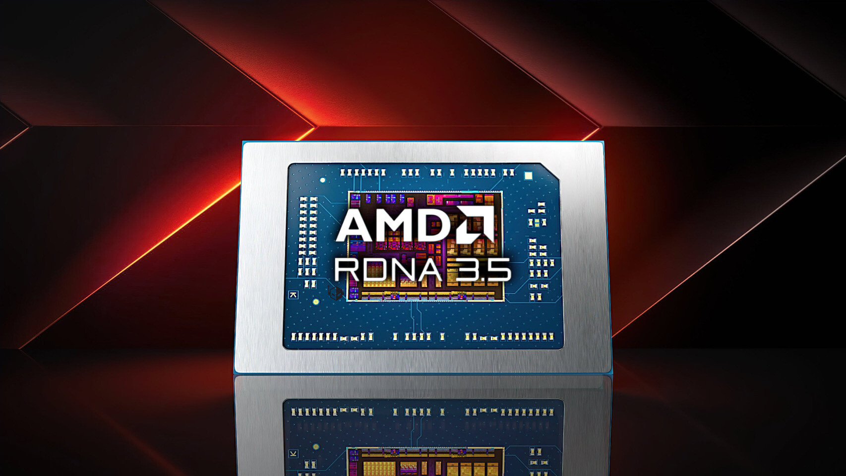
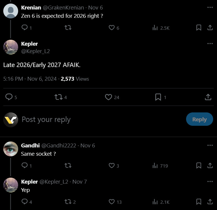
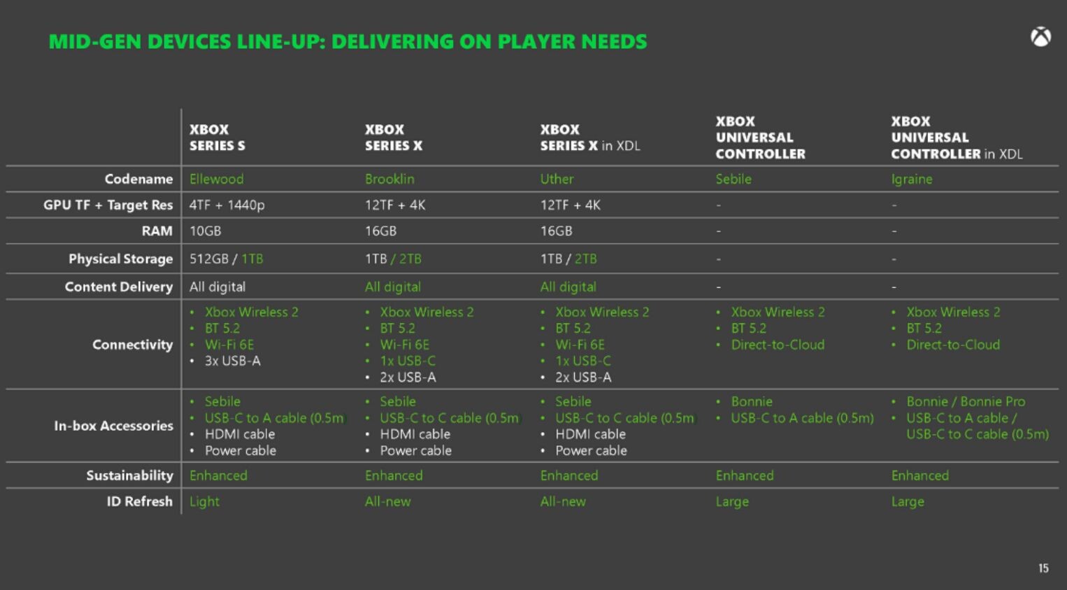
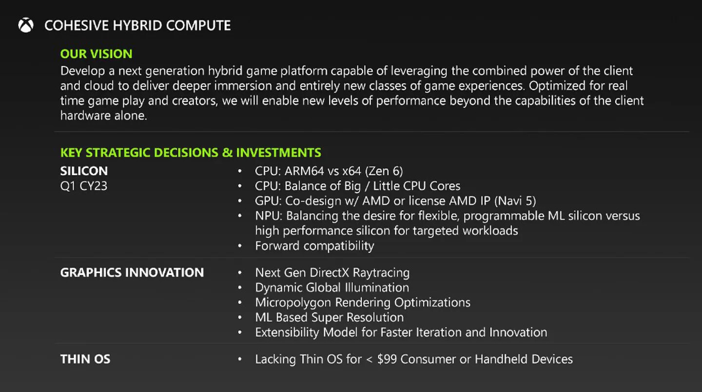
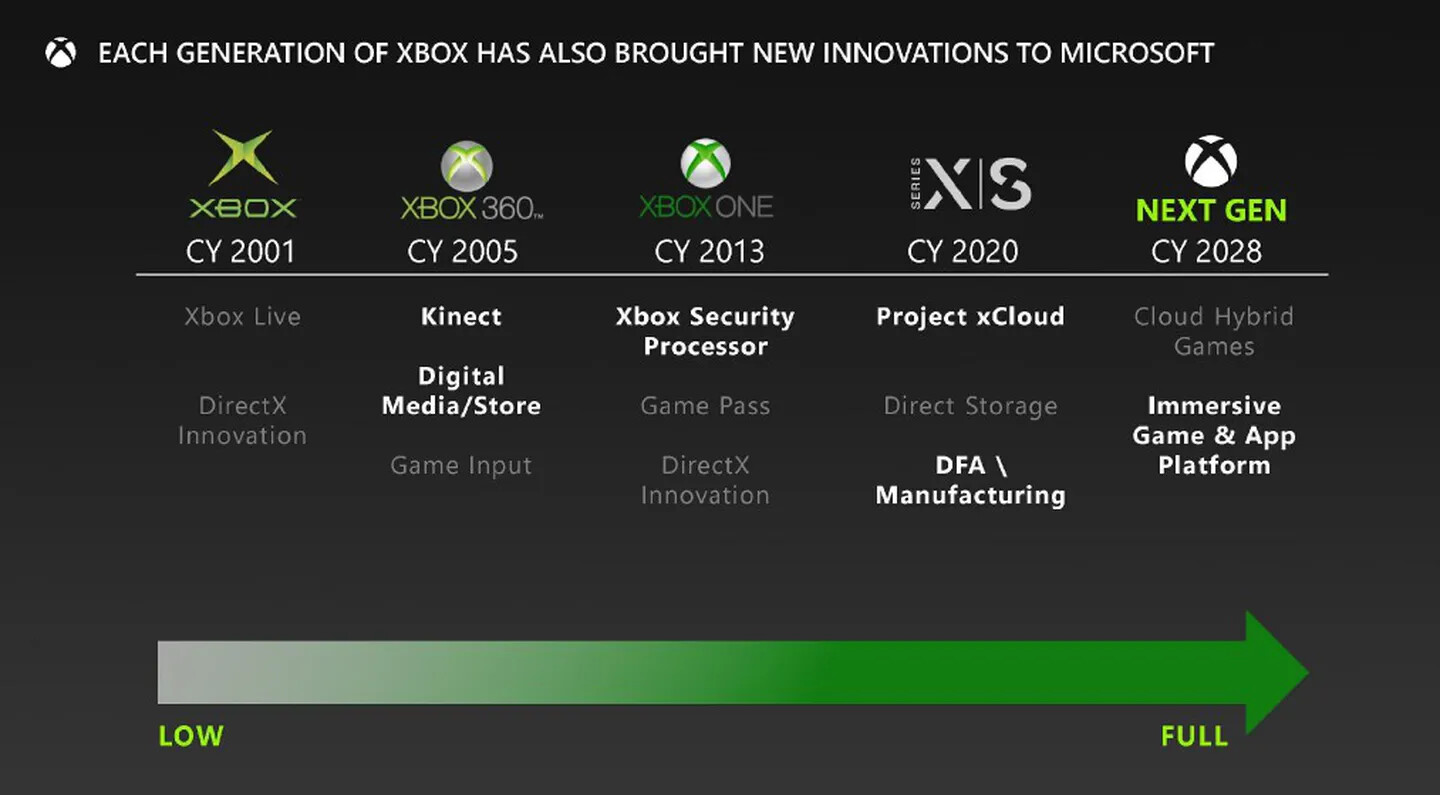
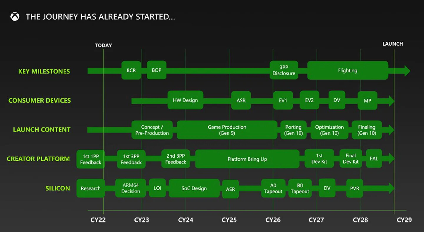
AMD UDNA Graphics Architecture to Power Next-Gen Xbox and PlayStation

AMD's next generation UDNA graphics architecture, which succeeds the current RDNA 4, will power the GPU of next generation Xbox and PlayStation consoles, VideoCardz reports. This would put the consoles a generation ahead of the Radeon RX 9000-series, and ready to take on some astoundingly complex AAA titles such as GTA 6. Kepler_L2, a reliable source with hardware leaks, has a some generational performance gain projections for UDNA over RDNA 4.

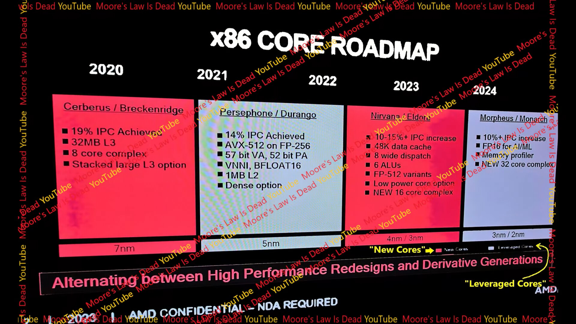
UDNA is expected to provide a 20% gain in raster performance per CU over RDNA 4, assuming other factors are comparable, such as memory and host platform. UDNA is also expected to offer a 2x ray tracing performance gain over RDNA 4. Kepler_L2 clarified that by this he means a halving in the frame-time incurred in having ray tracing enabled, compared to RDNA 4. What's emerging from these leaks is that the semi-custom SoCs powering next-generation consoles will be contemporary in terms of the architecture of its various IP blocks from AMD. Given that UDNA powers the GPU, the CPU could be equally advanced, based on at least "Zen 5" or "Zen 6," a significant upgrade over the "Zen 2" powering current consoles. There could be other inclusions, such as an NPU.

AMD Namedrops EPYC "Venice" Zen 6 and EPYC "Verano" Zen 7 Server Processors

AMD at its 2025 Advancing AI event name-dropped its two next generations of EPYC server processors to succeed the current EPYC "Turin" powered by Zen 5 microarchitecture. 2026 will see AMD debut the Zen 6 microarchitecture, and its main workhorse for the server segment will be EPYC "Venice." This processor will likely see a generational increase in CPU core counts, increased IPC from the full-sized Zen 6 cores, support for newer ISA, and an updated I/O package. AMD is looking to pack "Venice" with up to 256 CPU cores per package.

AMD is looking to increase the CPU core count per CCD (CPU complex die) with "Zen 6." The company plans to build these CCDs on the 2 nm TSMC N2 process node. The sIOD (server I/O die) of "Venice" implements PCI-Express Gen 6 for a generational doubling in bandwidth to GPUs, SSDs, and NICs. AMD is also claiming memory bandwidth as high as 1.6 TB/s. There are a couple of ways they can go about achieving this, either by increasing the memory clock speeds, or giving the processor a 16-channel DDR5 memory interface, up from the current 12-channel DDR5. The company could also add support for multichannel DIMM standards, such as MR-DIMM and MCR-DIMMs. All said and done, AMD is claiming a 70% increase in multithreaded performance over the current EPYC "Turin," which we assume is comparing the highest performing part to its next-gen successor.

Potential Next-gen AMD EPYC "Venice" CPU Identifier Turns Up in Linux Kernel Update

InstLatX64 has spent a significant chunk of time investigating AMD web presences; last month they unearthed various upcoming "Zen 5" processor families. This morning, a couple of mysterious CPU identifiers—"B50F00, B90F00, BA0F00, and BC0F00"—were highlighted in a social media post. According to screen-captured information, Team Red's Linux team seems to be patching in support for "Zen 6" technologies—InstLatX64 believes that the "B50F00" ID and internal "Weisshorn" codename indicate a successor to AMD's current-gen EPYC "Turin" server-grade processor series (known internally as "Breithorn"). Earlier in the month, a set of AIDA64 Beta update release notes mentioned preliminary support for "next-gen AMD desktop, server and mobile processors."

In a mid-April (2025) announcement, Dr. Lisa Su and colleagues revealed that their: "next-generation AMD EPYC processor, codenamed 'Venice,' is the first HPC product in the industry to be taped out and brought up on the TSMC advanced 2 nm (N2) process technology." According to an official "data center CPU" roadmap, "Venice" is on track to launch in 2026. Last month, details of "Venice's" supposed mixed configuration of "Zen 6" and "Zen 6C" cores—plus other technical tidbits—were disclosed via a leak. InstLatX64 and other watchdogs reckon that some of the latest identifiers refer to forthcoming "Venice-Dense" designs and unannounced Instinct accelerators.

Preliminary Support for AMD "Zen 6" Lands in AIDA64 Beta Update

Early indications of AMD's next-generation Ryzen processors have surfaced as AIDA64's newest beta release adds initial support for Ryzen 10000 "Zen 6" desktop, server, and mobile chips. The update was noted by X user HXL, suggesting that AMD has quietly shared basic specifications with developers of hardware monitoring software. Looking back, AIDA64 tends to announce chip support almost a year before official launches, so these new processors may not appear until Computex 2026. Leaks from March 2025 suggest that AMD's Zen 6 desktop lineup, currently codenamed Medusa Ridge, will remain compatible with the existing AM5 socket. This news should please PC enthusiasts because it means many users will not have to replace their motherboards when upgrading. Reports indicate that Medusa Ridge CPUs may include 12-core chiplet dies, marking a step forward from previous architectures.

These chips are expected to be manufactured using TSMC's N3P process, which is designed to deliver improved power efficiency and higher frequencies. Additionally, a Zen 6-based X3D series is likely to feature a 3D V-Cache, targeting gamers. A model like the Ryzen 7 10800X3D could follow the success of the 9800X3D by offering strong performance at its price. On the mobile side, "Medusa Point" processors are rumored to incorporate up to 22 hybrid cores that combine performance and efficiency cores under the Zen 6 architecture. However, these mobile chips seem to be further off, with a launch window set for late 2026 or early 2027. Although AIDA64's beta edition now recognizes Ryzen 10000 series chips, AMD's usual schedule suggests we will not see them in shops until mid-2026 at the earliest. Still, compatibility with AM5 and a move to a more advanced process promise meaningful improvements when Zen 6 finally arrives.

AMD EPYC "Venice" Leak: 2 nm Zen 6 and Zen 6c to Offer Up to 256C/512T and 1 GB of L3 in a Single Socket

AMD is preparing to set a new data-center performance bar with its upcoming 6th-generation EPYC "Venice" processors, built on the latest "Zen 6" and "Zen 6C" core designs and the industry's first 2 nm-class node from TSMC. Leaked engineering diagrams and forum reports suggest Venice will offer additional core scalability, memory capacity, and cache productivity for demanding server workloads. At the heart of the Venice platform lies a multi-chip module design featuring up to eight Core Complex Dies (CCDs) arrayed around one or more central I/O dies (IODs). In its Zen 6 configuration, each CCD houses 12 "classic" cores, yielding a maximum of 96 cores and 192 threads per socket. The cache per CCD is rumored to reach 128 MB of shared L3, double that of its predecessor, delivering up to 1 TB of L3 cache in a fully populated eight-CCD package.

For customers prioritizing raw thread count over per-core performance, the Zen 6C variant pushes the envelope to 256 "dense" cores and 512 threads by leveraging a leaner core design and higher CCD count. Despite the density boost, each Zen 6C core maintains 2 MB of L3 cache, preserving latency benefits even at scale. Memory bandwidth also receives a major uplift: Venice will support both 16-channel (SP7) and 12-channel (SP8) DDR5 configurations, accommodating up to 6 TB of system RAM per socket. The number of PCIe Gen 5 lanes is still unknown, but it could be well over 128 lanes, which the past 5th-generation EPYC CPUs had. Thermal and power targets differentiate the two sockets: SP7 models are expected to reach TDPs around 600 W, up from 400 W on current Zen 5 chips, while SP8 parts aim for 350-400 W to suit more moderate-density racks. This tiered approach will let hyperscalers and enterprise customers balance performance, efficiency, and cooling infrastructure, especially at the scale that hyperscalers have. A projected launch date is scheduled for late 2025 or early 2026.

Leaks Suggest AMD AM5 Future Support for Ryzen 9000G "Gorgon Point" & EPYC 4005 "Grado" CPUs

PC hardware watchers continue to pore over official AMD repositories and adjacent databases, in the hopes of finding unannounced next-gen technologies. Olrak29 and InstLatX64 have presented their latest Team Red-related findings; apparently reaching across futuristic desktop, mobile, and workstation product families. As outlined and interpreted by VideoCardz, several of these next-gen branches are already somewhat "known" properties—namely AMD's allegedly Zen 5-based Ryzen Threadripper "Shimada Peak" 9000WX (workstation) processor series. Following almost two years of leaks, an official introduction is expected to happen during Computex 2025. The Ryzen 9000G "Gorgon Point" desktop (Zen 5 + RDNA 3.5) APU series has turned up again; now "fully" linked to the AM5 socket platform (not a big surprise). The two leakers have also uncovered another rumored AM5-bound product lineup—"Grado" chips could be based on existing "Granite Ridge" foundations, but elevated to commercial/enterprise levels. These speculated basic/entry-level "EPYC 4005" processors are floated as natural successors to currently available 4004 forebears (related to Ryzen 7000 "Raphael" architecture).

Olrak29 and InstLatX64 have also found multiple mysterious FP8 socket-related Ryzen AI Mobile SoCs. "Krackan2" could be a cheaper refresh of current "Krackan Point" APUs—Tom's Hardware proposes smaller designs that sport fewer cores, and not configured with NPUs. Kepler_L2 has weighed in on the matter of three listed "Gorgon Point" IPs—he reckons that the third variant ("Gorgon Point3") will be a spin-off (aka refresh) of a "Krackan2" design. As suggested by insider knowledge, Team Red's convoluted scheme points to "Gorgon Point" being the sequel to "Strix Point." An FF5-based "Soundwave" processor design has appeared alongside the aforementioned futuristic Ryzen AI Mobile chipsets—industry whispers propose that AMD will be leveraging Arm architecture within a lower product tier. InstLatX64 pulled additional compelling information from AMD's Technical Information Portal—providing further insight into Ryzen AI "Medusa Point" APUs (Zen 6 + RDNA 3.5) being dreamt up, with a matching "larger footprint" FP10 platform.

AMD Ryzen AI "Medusa Point" APU Could Arrive with Larger Footprint - BGA "FP10" Dimensions Leaked

Shipping manifests have served as fairly reliable sources of pre-launch information—Everest (aka Olrak29) has discovered many juicy details in recent times. Their latest sleuthing session—combing through NBD documents—has indicated AMD's (alleged) prepping of a larger socket design for next-generation mobile processors. A leaked document alludes to the existence of various "MEDUSA01" jig and block "FP10" socket validation parts. Current-generation Ryzen AI "Strix Point" 300 series APUs utilize the FP8 socket format. Based on the "MEDUSA01" shipping manifest, it seems that a successor will arrive with a larger footprint—measurements of 25 mm x 42.5 mm are repeated throughout the leaked description list. Industry watchdogs surmise that "Medusa Point's" BGA FP10 socket will be approximately 6% larger than its predecessor.

Mid-way through last month, insider theorizations pointed to "Medusa Point" being a chiplet-based design. A "single 12-core Zen 6 CCD" was linked to a TSMC 3 nm-class node, with "N4P" reportedly selected for a separate mobile client I/O die. Readily available 4 nm Ryzen AI "Strix Point" processors are monolithic in nature. Initial inside track info mentioned RDNA 4 technology in the same equation as "Medusa Point," but recent Team Red's recent-ish targeting of "GFX1153" places RDNA 3.5 as the de facto choice.

AMD "Medusa Point" APU with Zen 6 Confirmed to Use RDNA 3.5, RDNA 4 Reserved for Discrete GPUs

AMD's next-generation Zen 6-based "Medusa Point" mobile APUs will not feature RDNA 4 graphics as previously speculated, according to recent code discoveries in AMD GPUOpen Drivers on GitHub. The Device ID "GfxIp12" associated with RDNA 4 architecture has been reserved only for discrete GPUs, confirming that the current Radeon RX 9000 series will exclusively implement AMD's latest graphics architecture. Current technical documentation indicates AMD will instead extend RDNA 3.5 implementation beyond the Zen 5 portfolio while potentially positioning UDNA as the successor technology for integrated graphics.

The chiplet-based Medusa Point design will reportedly pair a single 12-core Zen 6 CCD manufactured on TSMC's 3 nm-class node with a mobile client I/O die likely built on N4P. This arrangement is significantly different from current monolithic mobile solutions. Earlier speculation indicates the Medusa Point platform may support 3D V-Cache variants, leveraging the same vertical stacking methodology employed in current Zen 5 implementations. The mobile processor's memory controllers and neural processing unit are expected to receive substantial updates. However, compatibility limitations with AMD's latest graphics features, like FSR 4 technology, remain a concern due to the absence of RDNA 4 silicon. The Zen 6-powered Medusa Point processor family is scheduled for release in 2026, targeting premium mobile computing applications with a performance profile that builds upon AMD's current Strix Halo positioning.

AMD "Medusa Point" Mobile APU Design Linked to RDNA 3.X, Instead of RDNA 4

The "Medusa" or "Medusa Point" codename started to appear online over the past couple of months. These mysterious AMD projects were linked to next-generation "Zen 6" Ryzen desktop and mobile processor families (respectively). Initially, insiders reckoned that Team Red had selected an RDNA 4-based graphics solution for integration their futuristic new-gen laptop APU design. Two days ago, Golden Pig Upgrade weighed in with a different theory—the veteran leaker believes that provisions have regressed on the "Medusa Point" iGPU front.

Previous reports have suggested that the "Medusa Point" processor's iGPU aspect will utilize up to 16 compute units (CU), based on a theorized count of eight workgroup processors (WGPs) from leaked imagery. The latest insider tip points to the utilization of a non-specific "RDNA 3.x" branch, instead of conjectured RDNA 4 graphics technology. Industry watchdogs hold the belief that AMD will be sticking with RDNA 3.5 for a while—as featured on their current-gen "Zen 5" mobile-oriented Strix Point, Strix Halo and Krackan Point chips. As pointed out by Notebookcheck, Team Red leadership disclosed that RDNA 4 is exclusive to discrete card families (for the time being). RDNA 3.5-equipped APUs have—so far—received a warm welcome; AMD engineers could be reserving development resources for a distant future project.

AMD Advances openSIL Initiative Despite Minor Delays, Support for "Phoenix" and "Turin" CPUs Coming Soon

AMD's openSIL project, aimed towards open CPU silicon initialization code, continues progressing despite a slight delay in its development timeline. The initiative, which will eventually replace the current AGESA system across AMD's client and server processors, received a new update. The company initially targeted the end of 2024 to release proof-of-concept code for Phoenix client SoCs and Turin server hardware. However, as we move through the first quarter of 2025, AMD has acknowledged a slight deviation from this schedule. In a recent statement, AMD representatives assured the developer community that work continues steadily on both Phoenix and Turin proof-of-concept releases.

"We are hard at work preparing the Phoenix and Turin POC's for public release," stated an AMD representative, emphasizing that these releases will serve as sample code previewing future production-worthy implementations. The company clarified that these initial releases are not intended for production environments. The delay has minimal impact on AMD's plan, as the primary goal remains focused on achieving full production readiness with the upcoming Zen 6 architecture. The openSIL project promises to enhance Coreboot support and provide developers with full access to low-level system components. Though limited to select reference motherboards, the proof-of-concept releases will serve as the first milestones in AMD's journey toward more open hardware solutions.

AMD Zen 6 Powers "Medusa Point" Mobile and "Olympic Ridge" Desktop Processors

AMD is readying two important client segment processors powered by the next-generation "Zen 6" microarchitecture, according to a sensational new report by Moore's Law is Dead. These are the "Medusa Point" mobile processor, and the "Olympic Ridge" desktop. The former is a BGA roughly the size and Z-Height of the current "Strix Point," but the latter is being designed for the existing Socket AM5, making it the third (and probably final) microarchitecture to do so. If you recall, Socket AM4 served three generations of Zen, not counting the refreshed "Zen+." At the heart of the effort is a new CPU complex die (CCD) that AMD plans to use across its client and server lineup.

The "Zen 6" performance CCD is being designed for a 3 nm-class node, likely the TSMC N3E. This node promises a significant increase in transistor density, power, and clock speed improvements over the current TSMC N4P node being used to build the "Zen 5" CCD. Here's where it gets interesting. The CCD contains twelve full-sized "Zen 6" cores, marking the first increase in core-counts of AMD's performance cores since its very first "Zen" CCD. All 12 of these cores are part of a single CPU core complex (CCX), and share a common L3 cache. There could be a proportionate increase in cache size to 48 MB. AMD is also expected to improve the way the CCDs communicate with the I/O die and among each other.

AMD to Build Next-Gen I/O Dies on Samsung 4nm, Not TSMC N4P

Back in January, we covered a report about AMD designing its next-generation "Zen 6" CCDs on a 3 nm-class node by TSMC, and developing a new line of server and client I/O dies (cIOD and sIOD). The I/O die is a crucial piece of silicon that contains all the uncore components of the processor, including the memory controllers, the PCIe root complex, and Infinity Fabric interconnects to the CCDs and multi-socket connections. Back then it was reported that these new-generation I/O dies were being designed on the 4 nm silicon fabrication process, which was interpreted as being AMD's favorite 4 nm-class node, the TSMC N4P, on which the company builds everything from its current "Strix Point" mobile processors to the "Zen 5" CCDs. It turns out that AMD has other plans, and is exploring a 4 nm-class node by Samsung.

This node is very likely the Samsung 4LPP, also known as the SF4, which has been in mass-production since 2022. The table below shows how the SF4 compares with TSMC N4P and Intel 4, where it is shown striking a balance between the two. We have also added values for the TSMC N5 node from which the N4P is derived from, and you can see that the SF4 offers comparable transistor density to the N5, and is a significant improvement in transistor density over the TSMC N6, which AMD uses for its current generation of sIOD and cIOD. The new 4 nm node will allow AMD to reduce the TDP of the I/O die, implement a new power management solution, and more importantly, the need for a new I/O die is driven by the need for updated memory controllers that support higher DDR5 speeds and compatibility with new kinds of DIMMs, such as CUDIMMs, RDIMMs with RCDs, etc.

AMD to Build Zen 6 CCD on TSMC 3nm Process, Next-Gen cIOD and sIOD on 4nm

AMD is rumored to be building its next-generation CCD (core complex die) that implements the "Zen 6" microarchitecture, on the 3 nm TSMC N3E foundry node. This is part of a set of rumors from ChipHell forum, which got past rumors on AMD right. Apparently, AMD will also refresh the I/O dies for its next generation process, building them on the 4 nm foundry node, likely the TSMC N4C. The TSMC N3E node offers a 20% speed improvement, over 30% power savings, and approximately 60% logic density increase over TSMC N5, whereas the TSMC N4P node that the company uses for its current "Zen 5" chiplets only clock minor increases in logic density and power over N5. The N3E node relies on EUV double-patterning to achieve its logic density increases.

Perhaps the most interesting piece of news is the new-generation I/O dies. AMD is building these on the 4 nm node, which is a significant step up from the 6 nm node its current I/O dies are built on. On the client side of things, 4 nm will enable AMD to give the new cIOD an updated iGPU, probably based on a newer graphics architecture, such as RDNA 3.5. It will also give AMD the opportunity to integrate an NPU. The company might also update its key I/O components, such as the DDR5 memory controllers, to support higher memory speeds unlocked by CUDIMMs. We don't predict any updates on the PCIe front, since AMD is expected to carry on with Socket AM5, which determines that the cIOD puts out 28 PCIe Gen 5 lanes. At best, the USB interface put out from the processor could be updated to USB4 through an on-die host controller. Over on the server side, the new-generation sIOD will bring much needed increases to the DDR5 memory speeds enabled by clock drivers.

AMD "Zen 6" to Retain Socket AM5 for Desktops, 2026-27 Product Launches

The desktop version of AMD's next-generation "Zen 6" microarchitecture will retain Socket AM5, Kepler_L2, a reliable source with hardware leaks, revealed. What's more interesting is the rumor that the current "Zen 5" will remain AMD's mainstay for the entirety of 2025, and possibly even most of 2026, at least for the desktop platform. AMD will be banking heavily on the recently announced Ryzen 7 9800X3D, and its high core-count siblings, the Ryzen 9 9950X3D and possible 9900X3D, to see the company through for 2025 against Intel. The 9800X3D posted significantly higher gaming performance than Intel, and the 9950X3D is expected to be at least faster than the 7950X3D at gaming, which means its gaming performance, coupled with multithreaded application performance from its 16-core/32-thread count should be the face of AMD's desktop processor lineup for at least the next year.

It wouldn't be off-character for AMD to launch "Zen 6" on AM5, and not refresh the platform. The company had launched three microarchitectures (Zen thru Zen 3) on Socket AM4. With "Zen 6," AMD has the opportunity to not just increase IPC, but also core-counts per CCD, cache sizes, a new foundry node such as 3 nm, and probably even introduce features such as hybrid architecture and an NPU to the desktop platform, which means it could at least update the current 6 nm client I/O die (cIOD) while retaining AM5. A new cIOD could give AMD the much-needed opportunity to update the DDR5 memory controllers to support higher memory frequencies. The Kepler_L2 leak predicts a "late-2026 or early-2027" launch for desktop "Zen 6" processors. In the meantime, Intel is expected to ramp "Arrow Lake-S" on Socket LGA1851, and debut the "Panther Lake" microarchitecture on LGA1851 in 2025-26.

AMD OpenSIL Implementation (AGESA Replacement) On Track for 2025

OpenSIL is an open-source CPU initialization framework project that seeks to replace on-chip initialization microcode, such as AGESA, across both client- and server processors. AMD looks to implement OpenSIL as it makes its AMD EPYC processors more friendly to large customers that want to take control of this aspect of the processor. Since its open-sourcing in June 2023, AMD has come up with reference motherboards implementing OpenSIL, as well as modifying a Supermicro server motherboard to the architecture, to demo at conferences. AMD firmware engineer Paul Grimes presented the company's progress with implementing OpenSIL, at the OSFC conference, in Germany. It's been known that AMD is targeting a 2025-26 timeline for OpenSIL to hit product, but AMD put out specifics, such as its next-generation "Venice" server processor supporting OpenSIL.

"Venice" is codename for an AMD EPYC server processor generation succeeding "Turin." It is built on the future "Zen 6" microarchitecture, and AMD could at least unveil the processor some time in 2025, if not mass-produce it. late-2024 thru 2025 could see the company ramp up "Turin" and other server processors implementing "Zen 5." That's not all, AMD plans to being OpenSIL even to client processors, with the generation of Ryzen processors based on "Zen 6." This will see the AGESA microcode replaced by a first-party firmware from AMD based on OpenSIL, which PC OEMs will be able to customize. The biggest impact of this change will be felt in the commercial notebook and commercial desktop segments, where large organizations can take greater control over the chip initialization firmware.

AMD Zen 6 to Cram Up to 32 CPU Cores Per CCD

AMD's future "Zen 6" CPU microarchitecture is rumored to cram up to 32 cores per CCD (CPU complex die), or the common client/server chiplet with the CPU cores, according to Kepler_L2, a reliable source with hardware leaks. At this point it's not clear if they are referring to the regular "Zen 6" CPU core, or the physically compacted "Zen 6c" core meant for high core-count cloud server processors. The current pure "Zen 4c" CCD found in EPYC "Bergamo" processor packs 16 cores across two 8-core CCX (CPU core complexes) that share a 16 MB L3 cache among the 8 cores within the CCX. The upcoming "Zen 5c" CCD will pack 16 cores, but in a single 16-core CCX that shares 32 MB of L3 cache among the 16 cores for improved per-core cache access. "Zen 6" is expected to double this to 32 cores per CCD.

The 32-core CCD powered by "Zen 6" (likely Zen 6c), might take advantage of process improvements to double the core-count. At this point, it's not clear if this jumbo CCD features a single large CCX with all 32 cores sharing a large L3 cache; or if it's using two 16-core CCX that shares, say, 32 MB of L3 cache among the 16 cores. What's clear with this leak, though, is that AMD is looking to continue ramping up CPU core counts per socket. Data-centers and cloud customers seem to love this, and AMD is the only x86 processor maker in a serious competition with Arm-based server processor manufacturers such as Ampere, to increase significantly increase core counts per socket with each generation.

AMD's Strix Point Successor Codenamed "Sound Wave"?

Some of the earliest signs are emerging that AMD's mobile processor or desktop APU silicon that succeeds "Strix Point" being codenamed "Sound Wave." AMD tends to come up with quirky internal codenames for upcoming projects, mostly to zero in on the source of leaks, so "Sound Wave" as a codename is subject to change with time. While the upcoming 4 nm "Strix Point" and "Strix Halo" chips implement the "Zen 5" CPU microarchitecture and RDNA 3+ graphics architecture, besides XDNA 2 based NPU with a generational tripling in AI TOPS; Wccftech believes that "Sound Wave" could be an AMD processor of comparable class to "Strix Point," which implements the "Zen 6" CPU microarchitecture, which AMD has planned for a 2025-26 timeframe.

Perhaps the most interesting aspect of this leak is the foundry node, with the original source over at Korean tech blog Gamma0burst referencing 3 nm. This is the final node family from TSMC to implement FinFET transistors before the foundry transitions to nanosheets with N2. It's likely that AMD chooses one of the more advanced variants of TSMC's 3 nm nodes, such as the N3P or N3X, because 2025-26 will see rival Intel get close to introducing the Intel 20A foundry node for mass-production. Not much else is known about "Sound Wave" besides the "Zen 6" CPU cores at this point.

Zen 6 & RDNA 5 Linked to AMD "Medusa" Ryzen Client CPUs

The mysterious Zen 6 "Morpheus" processor architecture was leaked accidentally by an AMD engineer's LinkedIn profile—news outlets picked up on this information last April. Naturally, Team Red's next priority is Zen 5—the latest reports suggest that two different chiplet designs are penciled in for mass production within the second quarter of 2024. Last September, insiders claimed that a proposed EPYC 9006 "Venice" CPU series was based on the sixth-gen microarchitecture. Everest/Olrak_29 has revealed various bits of speculative material regarding futuristic "Ryzen Client" processor designs since the start of 2024.

The latest postings to social media posit that AMD has selected an RDNA 5-based integrated graphics solution (possibly occupying a tile), thus "skipping RDNA 4" on their "Medusa" lineup of Ryzen Client processors. Leaked Microsoft documents revealed that its Xbox hardware design division was considering RDNA 5 for next-gen console specs. Medusa's CPU aspect is allegedly populated by Zen 6 "Morpheus" cores—as claimed in a January tweet. A new package design was also riffed on at the time: "Yes, I have teased this before...Medusa will use 2.5D interconnect with a much higher bandwidth," instead of a "traditional" multi-die design. Industry speculation has AMD's Zen 6 client architecture linked to a loose 2025/2026 launch window.

AMD to Support AM5 Platform with New Products Till 2025 and Beyond

AMD continues to release new Ryzen 5000 series processor models for the Socket AM4 platform to this day, with new processors expected to launch next month. That's over 6 years of longevity for the platform, considering that AMD has extended official Ryzen 5000 series support all the way back to its first line of AM4 motherboards based on the 300-series chipset. The company plans a similar longevity for Socket AM5. In an interview with Overclockers UK, AMD's client channel business head David McAfee said "I think that we certainly recognized that the longevity of the AM4 platforms was one of the biggest reasons that led to the success of Ryzen and as we think and as we think about the future, 2025 and beyond, that decision to move to a next-generation of socket is one that's going to be really thought through really really carefully. We know the impact that moving to a new socket brings and we want to stay on AM5 for as long as we possibly can. We are firmly committed to 2025 and beyond and we will see how long that promise lasts beyond 2025."

AMD Socket AM5 is designed to deliver up to 230 W of package power, and has a contemporary I/O that includes a dual-channel DDR5 memory interface (4x 40-bit sub-channels); and 28 PCIe Gen 5 lanes (x16 PEG, two x4 NVMe, and x4 chipset bus), besides the usual SoC connectivity. With the upcoming Ryzen 8000G "Phoenix" APUs, we could expect to see that the socket even wires out modern display I/O such as DisplayPort 2.1 with USB type-C, and the bandwidth for 12-bit HDR up to 68 billion colors. AMD debuted Socket AM5 with the "Zen 4" microarchitecture, with "Zen 5" expected to launch in 2024. It's conceivable that the company's 2025 client architecture, "Zen 6," could also see its desktop presence on AM5, given that DDR5 memory and PCIe Gen 5 will remain relevant till at least that time.

Microsoft's Next-Gen Xbox for 2028 to Combine AMD Zen 6 and RDNA5 with a Powerful NPU and Cloud Integration

Microsoft Xbox Series X/S, their hardware refreshes, and variants, will reportedly be the company's mainstay all the way up until 2028, the company disclosed in its documents filed as part of its anti-trust lawsuit with the FTC. In a presentation slide titled "From "Zero Microsoft" to "Full Microsoft," the company explains how its next gen Xbox, scheduled for calendar year (CY) 2028, will see a full convergence of Microsoft co-developed hardware, software, and cloud compute services, into a powerful entertainment system. It elaborates on this in another slide, titled "Cohesive Hybrid Compute," where it states the company's vision to be the development of "a next generation hybrid game platform capable of leveraging the combined power of the client and cloud to deliver deeper immersion and entirely new classes of game experiences."

From the looks of it, Microsoft fully understands the creator economy that has been built over the gaming industry, and wants to develop its next-gen console to target exactly this—a single device from which people can play, stream, and create content from—something that's traditionally reserved for gaming desktop PCs. Game streamers playing on consoles usually have an entire creator PC setup handling the production and streaming side of things. Keeping this exact use-case in mind, Microsoft plans to "enable new levels of performance beyond the capabilities of the client hardware alone," by which it means that not only will the console rely on its own hardware—which could be jaw-dropping powerful as you'll see—but also leverage cloud compute services from Microsoft.

AMD Zen 5 Microarchitecture Referenced in Leaked Slides

A couple of slides from AMD's internal presentation were leaked to the web by Moore's Law is Dead, referencing what's allegedly the next-generation "Zen 5" microarchitecture. Internally, the performance variant of the "Zen 5" core is referred to as "Nirvana," and the CCD chiplet (CPU core die) based on "Nirvana" cores, is codenamed "Eldora." These CCDs will make up either the company's Ryzen "Granite Ridge" desktop processors, or EPYC "Turin" server processors. The cores themselves could also be part of the company's next-generation mobile processors, as part of heterogenous CCXs (CPU core complex), next to "Zen 5c" low-power cores.

In broad strokes, AMD describes "Zen 5" as introducing a 10% to 15% IPC increase over the current "Zen 4." The core will feature a larger 48 KB L1D cache, compared to the current 32 KB. As for the core itself, it features an 8-wide dispatch from the micro-op queue, compared to the 6-wide dispatch of "Zen 4." The integer execution stage gets 6 ALUs, compared to the current 4. The floating point unit gets FP-512 capabilities. Perhaps the biggest announcement is that AMD has increased the maximum cores per CCX from 8 to 16. At this point we don't know if it means that "Eldora" CCD will have 16 cores, or whether it means that the cloud-specific CCD with 16 "Zen 5c" cores will have 16 cores within a single CCX, rather than spread across two CCXs with smaller L3 caches. AMD is leveraging the TSMC 4 nm EUV node for "Eldora," the mobile processor based on "Zen 5" could be based on the more advanced TSMC 3 nm EUV node.

Leak Suggests Next-Gen Xbox Planned for 2028, AMD Zen 6 & RDNA 5 Considered

A comprehensive leak of documents—from a FTC versus Microsoft case—has exposed short and long-term plans in the world of Xbox. It seems that a relatively mild refresh of current generation Xbox Series X and S is lined up for the second half of 2024, but presentation material (dated April 2022) also reaches far into the future with strategies for next-gen gaming hardware. The bigwigs at Xbox were projecting a "full convergence" of their proprietary "xCloud" gaming platform and physical console hardware to deliver "cloud hybrid games" for 2028—schemes and priorities could have shifted in the interim, given various legal challenges and takeover bids.

One of the slides points to Microsoft getting the technical nitty-gritty sorted by CY2023—with two main options presented for consideration: a licensed ARM 64 design or a "Zen 6-based" AMD 64 processor. The next-gen Xbox's GPU aspect could incorporate a Navi 5 design (RDNA 5)—weighing up either a co-operation with AMD, or an IP license of said graphics architecture. VideoCardz theorizes that: "the latter option seems more likely if the ARM 64 chip is chosen over the Zen 6 APU." A key goal in this area seems to be an implementation of "Next-Gen DirectX Ray tracing" and "ML-based Super Resolutions" features. A Neural Processing Unit (NPU) is marked as a key provision for the 2028 console—granting some nice-to-have perks including: latency compensation, frame rate interpolation and various enrichments of the user experience.

Leak Suggests AMD 6th Gen EPYC "Venice" CPUs Linked to New SP7 Socket

Hardware leaker, YuuKi_AnS, has briefly turned their attention away from all things Team Blue—their latest leak points to upcoming server-grade processors chez AMD. A Zen 6 core-based 9006 EPYC CPU series, codenamed "Venice," is expected to arrive within two to three years along with an all-new SP7 socket—this information seems to have been sourced from an unnamed server manufacturer's product roadmap. A partial view of said slide also reveals forthcoming equipment powered by Intel "Falcon Shore" and NVIDIA "Blackwell" GPU technologies.

As reported a couple of months ago, older insider info has AMD using "Weisshorn" as an in-house moniker for Zen 6 "Morpheus" architecture, destined for Venice CPUs—alleged to form part of a 2025/2026 EPYC lineup. YuuKi_AnS proposes that these will utilize either 12-channel or 16-channel DDR5 memory configurations—thus providing plenty of bandwidth across hundreds of Zen cores. Altogether very handy for cloud, enterprise, and HPC workloads—industry experts reckon that 384-core counts are feasible on single packages. Naturally, a Team Red timeline dictates that Zen 5 "Nirvana" is due before Zen 6 "Morpheus," so EPYC 9005 "Turin(-X)" and 8005 "Turin-Dense" lineups are (allegedly) up for a 2024-ish launch window on SP5 (LGA-6096) and SP6 (LGA 4094) socket types.

AMD Zen 5 "Nirvana" and Zen 6 "Morpheus" Core Codenames Leaked, Confirm Foundry Nodes

An AMD engineer inadvertently leaked the core codenames of the company's upcoming "Zen 5" and "Zen 6" microarchitectures. It's important to understand here what has been leaked. "Zen 5" and "Zen 6" are microarchitecture names, just like the current "Zen 4" and past "Zen 3" or older. AMD uses codenames for the CCD (CPU complex dies) based on these microarchitectures, which it shares between Ryzen client and EPYC enterprise processors. For example, the CCD codename for "Zen 3" is "Brekenridge," and for "Zen 4" it is "Durango." AMD also uses codenames for the CPU cores themselves. "Zen 3" CPU cores are codenamed "Cerebrus," and "Zen 4" CPU cores "Persphone." And now, the leak:

The CCD based on the upcoming "Zen 5" microarchitecture is codenamed "Eldora," and the "Zen 5" CPU core itself is codenamed "Nirvana." There's no codename for the CCD based on "Zen 6," but its CPU cores are codenamed "Morpheus." The "Zen 5" microarchitecture will be based on the 3 nm EUV foundry node; while "Zen 6" will be 2 nm EUV. The engineer in the screenshot is contributing to the power-management technology behind "Zen 5" and "Zen 6," and states that their work on "Zen 5" spanned January-December of 2022, which means the development phase of the next "Zen" architecture is probably complete, and the architecture is undergoing testing and refinement. It's also claimed that work on at least the power-management aspect of "Zen 6" has started from January 2023.
Return to Keyword Browsing
Jul 4th, 2025 03:35 CDT change timezone

New Forum Posts

Popular Reviews

TPU on YouTube

Controversial News Posts