Apr 10th, 2025 04:12 EDT
change timezone
Latest GPU Drivers
New Forum Posts
- Do you use Linux? (572)
- Help with updating firmware on a AOC Agon Pro OLED monitor, says I need Install Tool (3)
- HP EliteDesk 800 G2 SFF CPU support (2)
- Anyone know where to get driver updates / backdates for TUF A15? (4)
- EK Quantum Velocity intel to amd conversion (13)
- [Update] FanControl (and other different monitoring software) blocked by Defender due to Winring0 vulnerability (1)
- How is the Gainward Phoenix Model in terms of quality? (0)
- ## [Golden Sample] RTX 5080 – 3300 MHz @ 1.020 V (Stock Curve) – Ultra-Stable & Efficient (44)
- hp envy 15 rtx 2060 max-q stock vbios (1)
- (Some of) What I'd like to See From a Final Fantasy IX Remake (10)
Popular Reviews
- The Last Of Us Part 2 Performance Benchmark Review - 30 GPUs Compared
- ASRock Z890 Taichi OCF Review
- MCHOSE L7 Pro Review
- Sapphire Radeon RX 9070 XT Pulse Review
- PowerColor Radeon RX 9070 Hellhound Review
- Upcoming Hardware Launches 2025 (Updated Apr 2025)
- Sapphire Radeon RX 9070 XT Nitro+ Review - Beating NVIDIA
- Acer Predator GM9000 2 TB Review
- ASUS GeForce RTX 5080 Astral OC Review
- UPERFECT UStation Delta Max Review - Two Screens In One
Controversial News Posts
- NVIDIA GeForce RTX 5060 Ti 16 GB SKU Likely Launching at $499, According to Supply Chain Leak (174)
- MSI Doesn't Plan Radeon RX 9000 Series GPUs, Skips AMD RDNA 4 Generation Entirely (146)
- Microsoft Introduces Copilot for Gaming (124)
- AMD Radeon RX 9070 XT Reportedly Outperforms RTX 5080 Through Undervolting (119)
- NVIDIA Reportedly Prepares GeForce RTX 5060 and RTX 5060 Ti Unveil Tomorrow (115)
- Over 200,000 Sold Radeon RX 9070 and RX 9070 XT GPUs? AMD Says No Number was Given (100)
- Nintendo Switch 2 Launches June 5 at $449.99 with New Hardware and Games (99)
- Nintendo Confirms That Switch 2 Joy-Cons Will Not Utilize Hall Effect Stick Technology (99)
News Posts matching #EUV
Return to Keyword Browsing
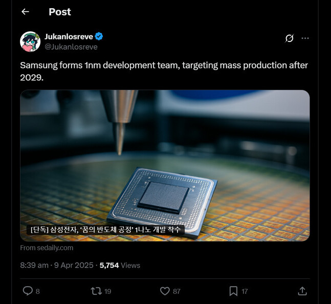
Insider Report Suggests Start of 1 nm Chip Development at Samsung, Alleged 2029 Mass Production Phase Targeted
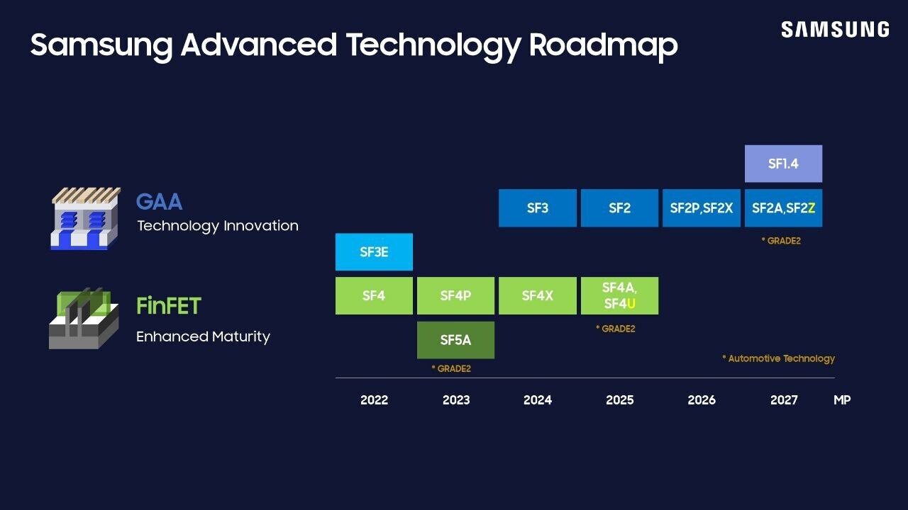
Samsung's foundry business seems to be busying itself with the rumored refinement of a 2 nm GAA (SF2) manufacturing node process—for possible mass production by the end of 2025, but company leadership will very likely be considering longer term goals. Mid-way through last month, industry moles posited that the megacorporation's semiconductor branch was questioning the future of a further out 1.4 nm (SF1.4) production line. Officially published roadmaps have this advanced technology rolling out by 2027. Despite present day "turmoil," insiders believe that a new team has been established—tasked with the creation of a so-called "dream semiconductor process." According to a fresh Sedaily news article, this fledgling department has started development of a 1 nm foundry process.
Anonymous sources claim that Samsung executives are keeping a watchful eye on a main competitor—as stated in the latest South Korean report: "there is a realistic gap with Taiwan's TSMC in technologies that are close to mass production, such as the 2 nm process, the company plans to speed up the development of the 1 nm process, a future technology, to create an opportunity for a turnaround." A portion of the alleged "1 nm development chip team" reportedly consists of veteran researchers from prior-gen projects. Semiconductor industry watchdogs theorize that a canceled SF1.4 line could be replaced by an even more advanced process. Sedaily outlined necessary hardware upgrades: "the 1.0 nanometer process requires a new technology concept that breaks the mold of existing designs as well as the introduction of next-generation equipment such as high-NA EUV exposure equipment. The company is targeting mass production after 2029." Samsung's current Advanced Technology Roadmap does not extend beyond 2027—inside sources claim that the decision to roll with 1.0 nm was made at some point last month.


Anonymous sources claim that Samsung executives are keeping a watchful eye on a main competitor—as stated in the latest South Korean report: "there is a realistic gap with Taiwan's TSMC in technologies that are close to mass production, such as the 2 nm process, the company plans to speed up the development of the 1 nm process, a future technology, to create an opportunity for a turnaround." A portion of the alleged "1 nm development chip team" reportedly consists of veteran researchers from prior-gen projects. Semiconductor industry watchdogs theorize that a canceled SF1.4 line could be replaced by an even more advanced process. Sedaily outlined necessary hardware upgrades: "the 1.0 nanometer process requires a new technology concept that breaks the mold of existing designs as well as the introduction of next-generation equipment such as high-NA EUV exposure equipment. The company is targeting mass production after 2029." Samsung's current Advanced Technology Roadmap does not extend beyond 2027—inside sources claim that the decision to roll with 1.0 nm was made at some point last month.


Tokyo Electron & IBM Renew Collaboration for Advanced Semiconductor Technology
This week, IBM and Tokyo Electron (TEL) announced an extension of their agreement for the joint research and development of advanced semiconductor technologies. The new 5-year agreement will focus on the continued advancement of technology for next-generation semiconductor nodes and architectures to power the age of generative AI. This agreement builds on a more than two-decade partnership between IBM and TEL for joint research and development. Previously, the two companies have achieved several breakthroughs, including the development of a new laser debonding process for producing 300 mm silicon chip wafers for 3D chip stacking technology.
Now, bringing together IBM's expertise in semiconductor process integration and TEL's leading-edge equipment, they will explore technology for smaller nodes and chiplet architectures to achieve the performance and energy efficiency requirements for the future of generative AI. "The work IBM and TEL have done together over the last 20 years has helped to push the semiconductor technology innovation to provide many generations of chip performance and energy efficiency to the semiconductor industry," said Mukesh Khare, GM of IBM Semiconductors and VP of Hybrid Cloud, IBM. "We are thrilled to be continuing our work together at this critical time to accelerate chip innovations that can fuel the era of generative AI."


Now, bringing together IBM's expertise in semiconductor process integration and TEL's leading-edge equipment, they will explore technology for smaller nodes and chiplet architectures to achieve the performance and energy efficiency requirements for the future of generative AI. "The work IBM and TEL have done together over the last 20 years has helped to push the semiconductor technology innovation to provide many generations of chip performance and energy efficiency to the semiconductor industry," said Mukesh Khare, GM of IBM Semiconductors and VP of Hybrid Cloud, IBM. "We are thrilled to be continuing our work together at this critical time to accelerate chip innovations that can fuel the era of generative AI."


Rapidus Confirms Launching 2nm Pilot Line in April, Mass Production Set for 2027
Rapidus Corporation today announced that its plans and budget for fiscal year 2025 have been approved by Japan's New Energy and Industrial Technology Development Organization (NEDO). The approval covers two commissioned projects under NEDO's "Post-5G Information and Communication Systems Infrastructure Enhancement R&D Project / Development of Advanced Semiconductor Manufacturing Technology (Commissioned)." These projects are the "Research and Development of 2 nm-Generation Semiconductor Integration Technology and short TAT (turnaround time) Manufacturing Technology Based on Japan-U.S. Collaboration" and "Development of Chiplet, Package Design and Manufacturing Technology for 2 nm-Generation Semiconductors."
The first of these projects, focused on front-end processes, was launched in November 2022 as part of Japan's next-generation semiconductor R&D effort. Under this program, Rapidus has continued construction of the Innovative Integration for Manufacturing (IIM) facility in Chitose, Hokkaido, which will serve as its production base. It also sent engineers to IBM in the U.S. to jointly develop 2 nm logic semiconductor mass production technologies and continued to achieve target performance as planned. Furthermore, Rapidus has installed EUV lithography and other production equipment at the IIM facility, and started cleanroom operation. As a result of these efforts, the company achieved its performance targets for FY2024.

The first of these projects, focused on front-end processes, was launched in November 2022 as part of Japan's next-generation semiconductor R&D effort. Under this program, Rapidus has continued construction of the Innovative Integration for Manufacturing (IIM) facility in Chitose, Hokkaido, which will serve as its production base. It also sent engineers to IBM in the U.S. to jointly develop 2 nm logic semiconductor mass production technologies and continued to achieve target performance as planned. Furthermore, Rapidus has installed EUV lithography and other production equipment at the IIM facility, and started cleanroom operation. As a result of these efforts, the company achieved its performance targets for FY2024.


SMIC Reportedly On Track to Finalize 5 nm Process in 2025, Projected to Cost 40-50% More Than TSMC Equivalent
According to a report produced by semiconductor industry analysts at Kiwoom Securities—a South Korean financial services firm—Semiconductor Manufacturing International Corporation (SMIC) is expected to complete the development of a 5 nm process at some point in 2025. Jukanlosreve summarized this projection in a recent social media post. SMIC is often considered to be China's flagship foundry business; the partially state-owned organization seems to heavily involved in the production of (rumored) next-gen Huawei Ascend 910 AI accelerators. SMIC foundry employees have reportedly struggled to break beyond a 7 nm manufacturing barrier, due to lack of readily accessible cutting-edge EUV equipment. As covered on TechPowerUp last month, leading lights within China's semiconductor industry are (allegedly) developing lithography solutions for cutting-edge 5 nm and 3 nm wafer production.
Huawei is reportedly evaluating an in-house developed laser-induced discharge plasma (LDP)-based machine, but finalized equipment will not be ready until 2026—at least for mass production purposes. Jukanlosreve's short interpretation of Kiwoom's report reads as follows: (SMIC) achieved mass production of the 7 nm (N+2) process without EUV and completed the development of the 5 nm process to support the mass production of the Huawei Ascend 910C. The cost of SMIC's 5 nm process is 40-50% higher than TSMC's, and its yield is roughly one-third." The nation's foundries are reliant on older ASML equipment, thus are unable to produce products that can compete with the advanced (volume and quality) output of "global" TSMC and Samsung chip manufacturing facilities. The fresh unveiling of SiCarrier's Color Mountain series has signalled a promising new era for China's foundry industry.

Huawei is reportedly evaluating an in-house developed laser-induced discharge plasma (LDP)-based machine, but finalized equipment will not be ready until 2026—at least for mass production purposes. Jukanlosreve's short interpretation of Kiwoom's report reads as follows: (SMIC) achieved mass production of the 7 nm (N+2) process without EUV and completed the development of the 5 nm process to support the mass production of the Huawei Ascend 910C. The cost of SMIC's 5 nm process is 40-50% higher than TSMC's, and its yield is roughly one-third." The nation's foundries are reliant on older ASML equipment, thus are unable to produce products that can compete with the advanced (volume and quality) output of "global" TSMC and Samsung chip manufacturing facilities. The fresh unveiling of SiCarrier's Color Mountain series has signalled a promising new era for China's foundry industry.


Chinese Researchers Develop No-Silicon 2D GAAFET Transistor Technology
Scientists from Beijing University have developed the world's first two-dimensional gate-all-around field-effect transistor (GAAFET), establishing a new performance benchmark in domestic semiconductor design. The design, documented in Nature, represents a difference in transistor architecture that could reshape the future of Chinese microelectronics design. Given the reported characteristic of 40% higher performance and 10% improved efficiency compared to the TSMC 3 nm N3 node, it looks rather promising. The research team, headed by Professors Peng Hailin and Qiu Chenguang, engineered a "wafer-scale multi-layer-stacked single-crystalline 2D GAA configuration" that demonstrated superior performance metrics when benchmarked against current industry leaders. The innovation leverages bismuth oxyselenide (Bi₂O₂Se), a novel semiconductor material that maintains exceptional carrier mobility at sub-nanometer dimensions—a critical advantage as the industry struggles to push angstrom-era semiconductor nodes.
"Traditional silicon-based transistors face fundamental physical limitations at extreme scales," explained Professor Peng, who characterized the technology as "the fastest, most efficient transistor ever developed." The 2D GAAFET architecture circumvents the mobility degradation that plagues silicon in ultra-small geometries, allowing for continued performance scaling beyond current nodes. The development comes during China's intensified efforts to achieve semiconductor self-sufficiency, as trade restrictions have limited access to advanced lithography equipment and other critical manufacturing technologies. Even with China developing domestic EUV technology, it is still not "battle" proven. Rather than competing directly with established fabrication processes, the Beijing team has pioneered an entirely different technological approach—what Professor Peng described as "changing lanes entirely" rather than seeking incremental improvements, where China can not compete in the near term.
"Traditional silicon-based transistors face fundamental physical limitations at extreme scales," explained Professor Peng, who characterized the technology as "the fastest, most efficient transistor ever developed." The 2D GAAFET architecture circumvents the mobility degradation that plagues silicon in ultra-small geometries, allowing for continued performance scaling beyond current nodes. The development comes during China's intensified efforts to achieve semiconductor self-sufficiency, as trade restrictions have limited access to advanced lithography equipment and other critical manufacturing technologies. Even with China developing domestic EUV technology, it is still not "battle" proven. Rather than competing directly with established fabrication processes, the Beijing team has pioneered an entirely different technological approach—what Professor Peng described as "changing lanes entirely" rather than seeking incremental improvements, where China can not compete in the near term.


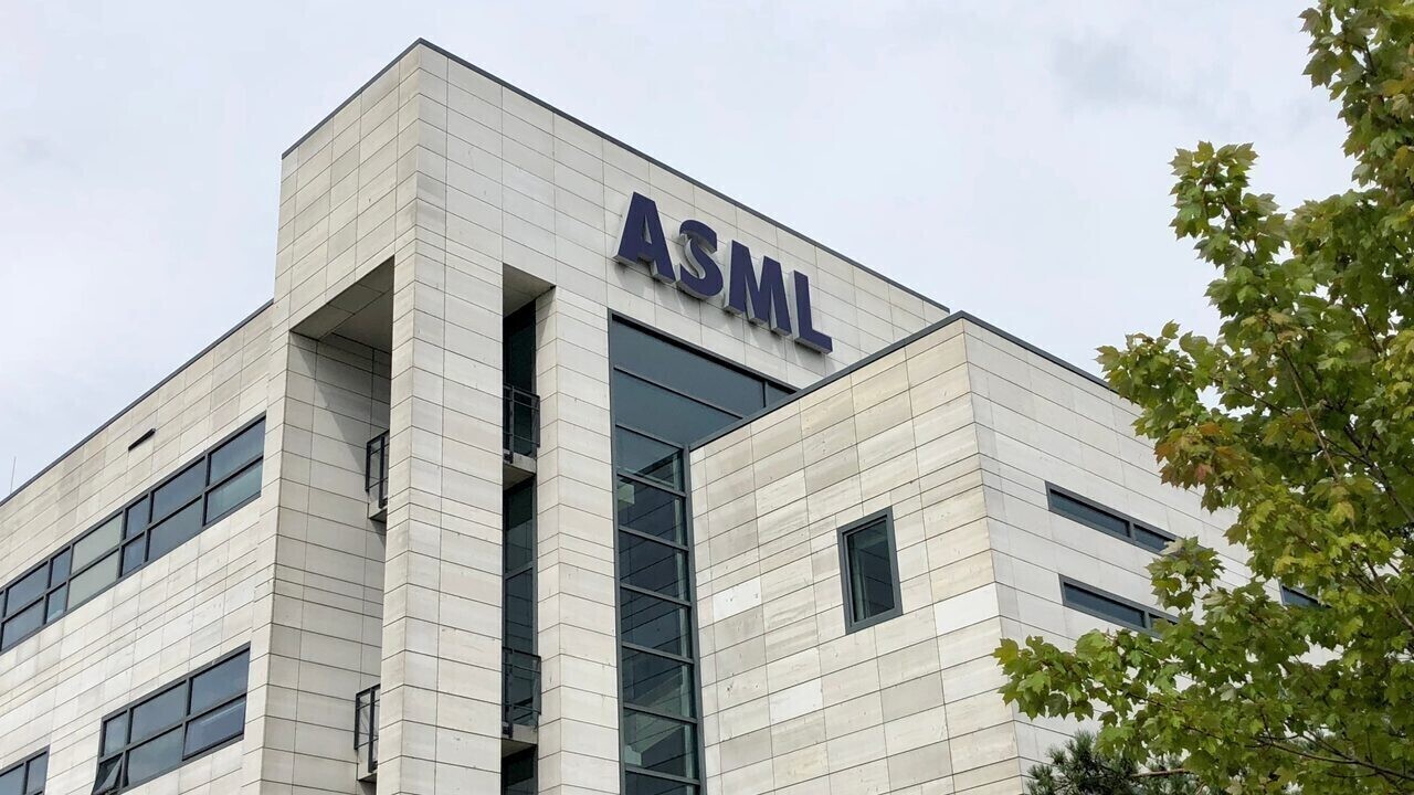
ASML and imec Sign Strategic Partnership Agreement to Support Semiconductor Research and Sustainable Innovation in Europe
ASML Holding N.V. (ASML) and imec, a leading research and innovation hub in nanoelectronics and digital technologies, today announce that they have signed a new strategic partnership agreement, focusing on research and sustainability. The agreement has a duration of five years and aims to deliver valuable solutions in two areas by bringing together ASML's and imec's respective knowledge and expertise. First, to develop solutions that advance the semiconductor industry and second, to develop initiatives focused on sustainable innovation.
The collaboration incorporates ASML's whole product portfolio, with a focus on developing high-end nodes, using ASML systems including 0.55 NA EUV, 0.33 NA EUV, DUV immersion, YieldStar optical metrology and HMI single- and multi-beam technologies. These tools will be installed in imec's state-of-the-art pilot line and incorporated in the EU- and Flemish-funded NanoIC pilot line, providing the most advanced infrastructure for sub-2 nm R&D to the international semiconductor ecosystem. Focus areas for R&D will also include silicon photonics, memory and advanced packaging, offering full stack innovation for future semiconductor-based AI applications in diverse markets.
The collaboration incorporates ASML's whole product portfolio, with a focus on developing high-end nodes, using ASML systems including 0.55 NA EUV, 0.33 NA EUV, DUV immersion, YieldStar optical metrology and HMI single- and multi-beam technologies. These tools will be installed in imec's state-of-the-art pilot line and incorporated in the EU- and Flemish-funded NanoIC pilot line, providing the most advanced infrastructure for sub-2 nm R&D to the international semiconductor ecosystem. Focus areas for R&D will also include silicon photonics, memory and advanced packaging, offering full stack innovation for future semiconductor-based AI applications in diverse markets.

Huawei Obtained Two Million Ascend 910B Dies from TSMC via Shell Companies to Circumvent US Sanctions
According to a recent Center for Strategic and International Studies report, Huawei got its hand on approximately two million Ascend 910B logic dies through shell companies that misled TSMC. This acquisition violates US export controls designed to restrict China's access to advanced semiconductor technology. The report details how Huawei leveraged intermediaries to procure chiplets for its AI accelerators before TSMC discovered the deception and halted shipments. These components are critical for Huawei's AI hardware roadmap, which progressed from the original Ascend 910 (manufactured by TSMC on N7+ until 2020) to the domestically produced Ascend 910B and 910C chips fabricated at SMIC using first and second-generation 7 nm-class technologies, respectively. Huawei reportedly wanted TSMC-made dies because of manufacturing challenges in domestic chip production. The Ascend 910B and 910C reportedly suffer from poor yields, with approximately 25% of units failing during the advanced packaging process that combines compute dies with HBM memory.
Despite these challenges, the performance gap with market-leading solutions still remains but has narrowed considerably, with the Ascend 910C reportedly delivering 60% of NVIDIA H100's performance. Huawei has executed a strategic stockpiling initiative, particularly for high-bandwidth memory components. The company likely acquired substantial HBM inventory between August and December 2024, when restrictions on advanced memory sales to China were announced but not yet implemented. The semiconductor supply chain breach shows that enforcing technology export controls is challenging, and third parties can still purchase silicon for restricted companies. While Huawei continues building AI infrastructure for both internal projects and external customers, manufacturing constraints may limit its ability to scale deployments against competitors with access to more advanced manufacturing processes. Perhaps a future domestic EUV-based silicon manufacturing flow will allow Huawei to gain access to more advanced domestic production, completely circumventing US-imposed restrictions.
Despite these challenges, the performance gap with market-leading solutions still remains but has narrowed considerably, with the Ascend 910C reportedly delivering 60% of NVIDIA H100's performance. Huawei has executed a strategic stockpiling initiative, particularly for high-bandwidth memory components. The company likely acquired substantial HBM inventory between August and December 2024, when restrictions on advanced memory sales to China were announced but not yet implemented. The semiconductor supply chain breach shows that enforcing technology export controls is challenging, and third parties can still purchase silicon for restricted companies. While Huawei continues building AI infrastructure for both internal projects and external customers, manufacturing constraints may limit its ability to scale deployments against competitors with access to more advanced manufacturing processes. Perhaps a future domestic EUV-based silicon manufacturing flow will allow Huawei to gain access to more advanced domestic production, completely circumventing US-imposed restrictions.

China Develops Domestic EUV Tool, ASML Monopoly in Trouble
China's domestic extreme ultraviolet (EUV) lithography development is far from a distant dream. The newest system, now undergoing testing at Huawei's Dongguan facility, leverages laser-induced discharge plasma (LDP) technology, representing a potentially disruptive approach to EUV light generation. The system is scheduled for trial production in Q3 2025, with mass manufacturing targeted for 2026, potentially positioning China to break ASML's technical monopoly in advanced lithography. The LDP approach employed in the Chinese system generates 13.5 nm EUV radiation by vaporizing tin between electrodes and converting it to plasma via high-voltage discharge, where electron-ion collisions produce the required wavelength. This methodology offers several technical advantages over ASML's laser-produced plasma (LPP) technique, including simplified architecture, reduced footprint, improved energy efficiency, and potentially lower production costs.
The LPP method relies on high-energy lasers and complex FPGA-based real-time control electronics to achieve the same result. While ASML has refined its LPP-based systems over decades, the inherent efficiency advantages of the LDP approach could accelerate China's catch-up timeline in this critical semiconductor manufacturing technology. When the US imposed sanctions on EUV shipments to Chinese companies, the Chinese semiconductor development was basically limited as standard deep ultraviolet (DUV) wave lithography systems utilize 248 nm (KrF) and 193 nm (ArF) wavelengths for semiconductor patterning, with 193 nm immersion technology representing the most advanced pre-EUV production technique. These longer wavelengths contrast with EUV's 13.5 nm radiation, requiring multiple patterning techniques to achieve advanced nodes.

The LPP method relies on high-energy lasers and complex FPGA-based real-time control electronics to achieve the same result. While ASML has refined its LPP-based systems over decades, the inherent efficiency advantages of the LDP approach could accelerate China's catch-up timeline in this critical semiconductor manufacturing technology. When the US imposed sanctions on EUV shipments to Chinese companies, the Chinese semiconductor development was basically limited as standard deep ultraviolet (DUV) wave lithography systems utilize 248 nm (KrF) and 193 nm (ArF) wavelengths for semiconductor patterning, with 193 nm immersion technology representing the most advanced pre-EUV production technique. These longer wavelengths contrast with EUV's 13.5 nm radiation, requiring multiple patterning techniques to achieve advanced nodes.


Intel's High-NA EUV Machines Already Processed 30,000 Wafers, More to Come with 14A Node
Intel has successfully deployed two advanced ASML High-NA Twinscan EXE:5000 EUV lithography systems at its D1 development facility near Hillsboro, Oregon, processing approximately 30,000 wafers in a single quarter. The High-NA EUV systems, each reportedly valued at $380 million, represent a substantial improvement over previous lithography tools, achieving resolution down to 8 nm with a single exposure compared to the 13.5 nm resolution of current Low-NA systems. Early operational data indicates these machines are approximately twice as reliable as previous EUV generations, addressing reliability challenges that previously hampered Intel's manufacturing progress. The ability to accomplish with a single exposure what previously required three exposures and approximately 40 processing steps has been reduced to just "single digit" processing steps.
Intel has historically been an early adopter of high-NA EUV lithography, a much more aggressive strategy than its competitors like TSMC, which manufactures its advanced silicon using low-NA EUV tools. The company plans to utilize these systems for its upcoming 14A chip manufacturing process, though no specific mass production date has been announced. While ASML classifies these Twinscan EXE:5000 systems as pre-production tools not designed for high-volume manufacturing, Intel's extensive wafer processing is more of a test bed. The early adoption provides Intel with valuable development opportunities across various High-NA EUV manufacturing aspects, including photomask glass, pellicles, and specialized chemicals that could establish future industry standards. Intel's current 18A node is utilizing Low-NA lithography tools, where Intel is only exploring High-NA with it for testing, before moving on to 14A high-volume manufacturing with High-NA EUV.
Intel has historically been an early adopter of high-NA EUV lithography, a much more aggressive strategy than its competitors like TSMC, which manufactures its advanced silicon using low-NA EUV tools. The company plans to utilize these systems for its upcoming 14A chip manufacturing process, though no specific mass production date has been announced. While ASML classifies these Twinscan EXE:5000 systems as pre-production tools not designed for high-volume manufacturing, Intel's extensive wafer processing is more of a test bed. The early adoption provides Intel with valuable development opportunities across various High-NA EUV manufacturing aspects, including photomask glass, pellicles, and specialized chemicals that could establish future industry standards. Intel's current 18A node is utilizing Low-NA lithography tools, where Intel is only exploring High-NA with it for testing, before moving on to 14A high-volume manufacturing with High-NA EUV.


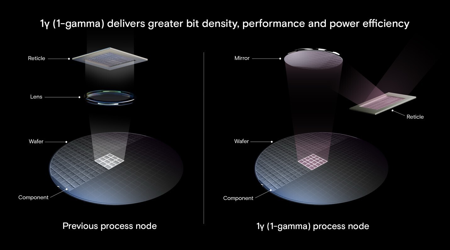
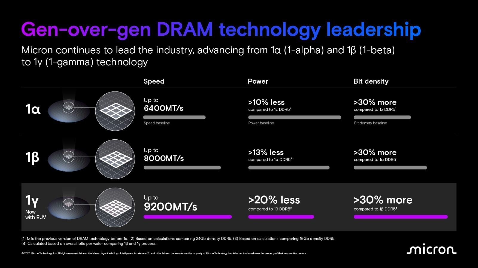
Micron Announces Shipment of 1γ (1-gamma) DRAM: Company's First EUV Memory Node
Micron Technology, Inc., today announced it is the first in the industry to ship samples of its 1γ (1-gamma), sixth-generation (10 nm-class) DRAM node-based DDR5 memory designed for next-generation CPUs to ecosystem partners and select customers. This 1γ DRAM milestone builds on Micron's previous 1α (1-alpha) and 1β (1-beta) DRAM node leadership to deliver innovations that will power future computing platforms from the cloud to industrial and consumer applications to Edge AI devices like AI PCs, smartphones and automobiles. The Micron 1γ DRAM node will first be leveraged in its 16 Gb DDR5 DRAM and over time will be integrated across Micron's memory portfolio to meet the industry's accelerating demand for high-performance, energy-efficient memory solutions for AI. Designed to offer speed capabilities of up to 9200 MT/s, the 16 Gb DDR5 product provides up to a 15% speed increase and over 20% power reduction compared to its predecessor.


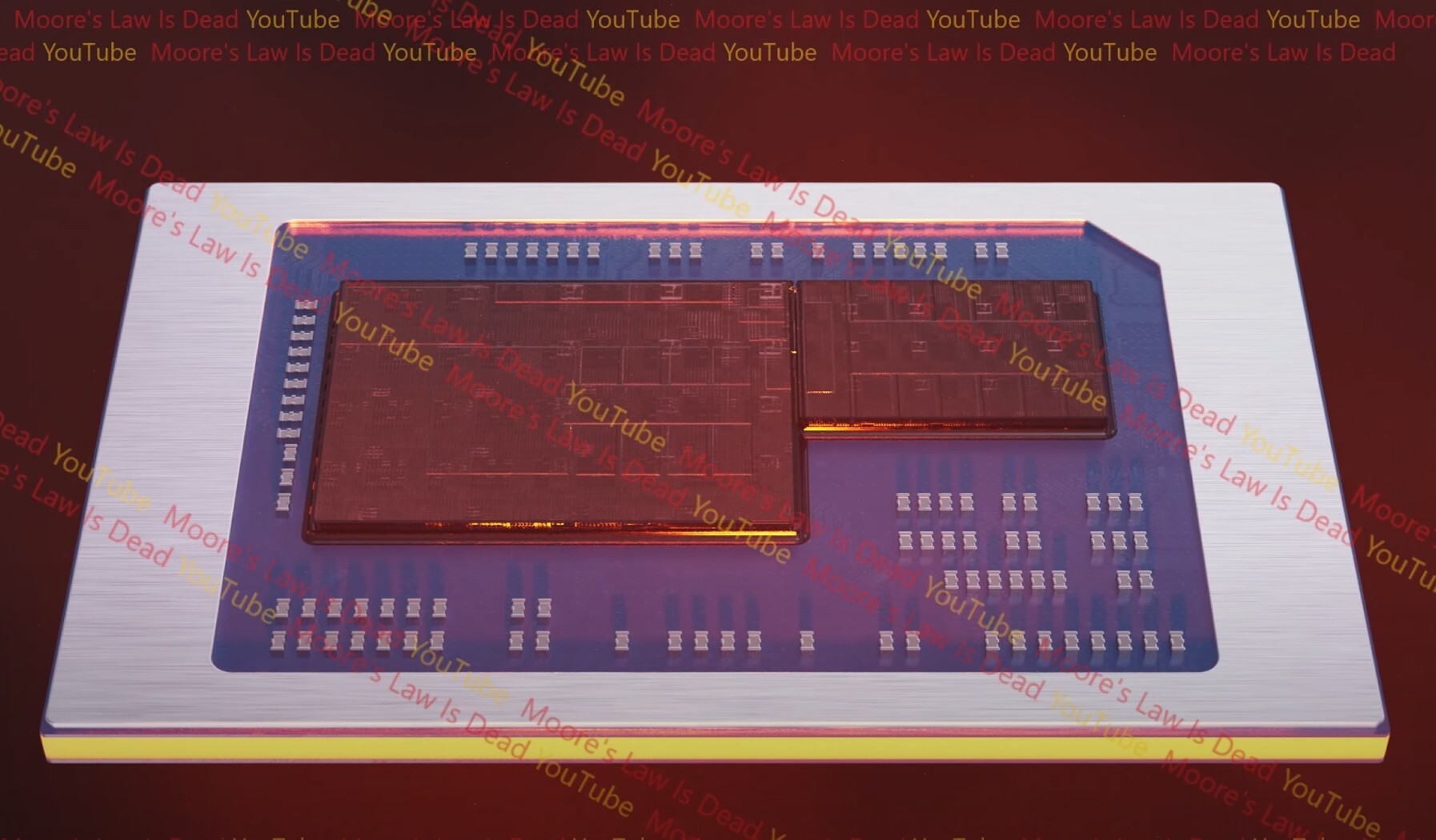
AMD Zen 6 Powers "Medusa Point" Mobile and "Olympic Ridge" Desktop Processors
AMD is readying two important client segment processors powered by the next-generation "Zen 6" microarchitecture, according to a sensational new report by Moore's Law is Dead. These are the "Medusa Point" mobile processor, and the "Olympic Ridge" desktop. The former is a BGA roughly the size and Z-Height of the current "Strix Point," but the latter is being designed for the existing Socket AM5, making it the third (and probably final) microarchitecture to do so. If you recall, Socket AM4 served three generations of Zen, not counting the refreshed "Zen+." At the heart of the effort is a new CPU complex die (CCD) that AMD plans to use across its client and server lineup.
The "Zen 6" performance CCD is being designed for a 3 nm-class node, likely the TSMC N3E. This node promises a significant increase in transistor density, power, and clock speed improvements over the current TSMC N4P node being used to build the "Zen 5" CCD. Here's where it gets interesting. The CCD contains twelve full-sized "Zen 6" cores, marking the first increase in core-counts of AMD's performance cores since its very first "Zen" CCD. All 12 of these cores are part of a single CPU core complex (CCX), and share a common L3 cache. There could be a proportionate increase in cache size to 48 MB. AMD is also expected to improve the way the CCDs communicate with the I/O die and among each other.


The "Zen 6" performance CCD is being designed for a 3 nm-class node, likely the TSMC N3E. This node promises a significant increase in transistor density, power, and clock speed improvements over the current TSMC N4P node being used to build the "Zen 5" CCD. Here's where it gets interesting. The CCD contains twelve full-sized "Zen 6" cores, marking the first increase in core-counts of AMD's performance cores since its very first "Zen" CCD. All 12 of these cores are part of a single CPU core complex (CCX), and share a common L3 cache. There could be a proportionate increase in cache size to 48 MB. AMD is also expected to improve the way the CCDs communicate with the I/O die and among each other.


ASML Reports €28.3 Billion Total Net Sales and €7.6 Billion Net Income in 2024
Today, ASML Holding NV (ASML) has published its 2024 fourth-quarter and full-year results.
"Our fourth-quarter was a record in terms of revenue, with total net sales coming in at €9.3 billion, and a gross margin of 51.7%, both above our guidance. This was primarily driven by additional upgrades. We also recognized revenue on two High NA EUV systems. We shipped a third High NA EUV system to a customer in the fourth quarter.

- Q4 total net sales of €9.3 billion, gross margin of 51.7%, net income of €2.7 billion
- Quarterly net bookings in Q4 of €7.1 billion of which €3.0 billion is EUV
- 2024 total net sales of €28.3 billion, gross margin of 51.3%, net income of €7.6 billion
- ASML expects Q1 2025 total net sales between €7.5 billion and €8.0 billion, and a gross margin between 52% and 53%
- ASML expects 2025 total net sales to be between €30 billion and €35 billion, with a gross margin between 51% and 53%
"Our fourth-quarter was a record in terms of revenue, with total net sales coming in at €9.3 billion, and a gross margin of 51.7%, both above our guidance. This was primarily driven by additional upgrades. We also recognized revenue on two High NA EUV systems. We shipped a third High NA EUV system to a customer in the fourth quarter.


Fujifilm Pumps ¥100 Billion in Semiconductor Material Expansion to Meet Chip Demand
According to Nikkei, Fujifilm Holdings is reportedly set to invest ¥100 billion ($640.5 million) by March 2027 to expand production capacities in the U.S., Japan, South Korea, and India. The main focus of the expansion is semiconductor materials, which are vital for the modern semiconductor supply chain. While the company has not officially confirmed the plan, it follows global efforts to straighten material supply chains as chipmakers ramp up the construction of cutting-edge fabs in these regions. The investment, doubling Fujifilm's semiconductor materials spending over the past three years, targets rising demand driven by new fabs from Intel, TSMC, Samsung, and SK Hynix, particularly for AI and HPC. Fujifilm, ranked fifth globally in photosensitive materials, is one of only five companies worldwide producing ultra-pure photoresists for extreme ultraviolet (EUV) lithography.
These photoresists must meet rigorous standards due to EUV's 13.5 nm wavelength, requiring precision in sensitivity, resolution, and compatibility with mask materials. Fujifilm strategically locates facilities near major hubs to strengthen partnerships with key clients. In Japan, a ¥13 billion ($83.27 million) plant in Shizuoka Prefecture is underway, while a South Korean site in Pyeongtaek will receive upgraded equipment by autumn. A Cheonan facility, set for spring 2027, aims to boost the output of chemical mechanical planarization (CMP) agents by 30%. The company also eyes India's emerging semiconductor sector, exploring partnerships or joint ventures to establish local production post-2027.
These photoresists must meet rigorous standards due to EUV's 13.5 nm wavelength, requiring precision in sensitivity, resolution, and compatibility with mask materials. Fujifilm strategically locates facilities near major hubs to strengthen partnerships with key clients. In Japan, a ¥13 billion ($83.27 million) plant in Shizuoka Prefecture is underway, while a South Korean site in Pyeongtaek will receive upgraded equipment by autumn. A Cheonan facility, set for spring 2027, aims to boost the output of chemical mechanical planarization (CMP) agents by 30%. The company also eyes India's emerging semiconductor sector, exploring partnerships or joint ventures to establish local production post-2027.

Lam Research Establishes 28nm Pitch in High-Resolution Patterning Through Dry Photoresist Technology
Lam Research Corporation today announced that its innovative dry photoresist (dry resist) technology has been qualified for direct-print 28 nm pitch back end of line (BEOL) logic at 2 nm and below by imec, a leading research and innovation hub in nanoelectronics and digital technologies. An advanced patterning technique introduced by Lam, dry resist enhances the resolution, productivity and yield of extreme ultraviolet (EUV) lithography, a pivotal technology used in the production of next-generation semiconductor devices.
"Lam's dry photoresist technology provides unparalleled low-defectivity, high-resolution patterning," said Vahid Vahedi, chief technology and sustainability officer at Lam Research. "We are excited to offer this technology to imec and its partners as a critical process in the design and manufacturing of leading-edge semiconductor devices."
"Lam's dry photoresist technology provides unparalleled low-defectivity, high-resolution patterning," said Vahid Vahedi, chief technology and sustainability officer at Lam Research. "We are excited to offer this technology to imec and its partners as a critical process in the design and manufacturing of leading-edge semiconductor devices."

Rapidus Installs Japan's First ASML NXE:3800E EUV Lithography Machine
Rapidus Corporation, a manufacturer of advanced logic semiconductors, today announced the delivery and installation of ASML's EUV lithography equipment at its Innovative Integration for Manufacturing (IIM-1) foundry, an advanced semiconductor development and manufacturing fab currently under construction in Chitose, Hokkaido. To commemorate the installation, a ceremony was held at Portom Hall in the New Chitose Airport.
This is a significant milestone for Japan's semiconductor industry, marking the first time that an EUV lithography tool will be used for mass production in the country. In addition to the EUV lithography machinery, Rapidus will install additional complementary advanced semiconductor manufacturing equipment, as well as full automated material handling systems in its IIM-1 foundry to optimize 2 nm generation gate-all-around (GAA) semiconductor manufacturing.

This is a significant milestone for Japan's semiconductor industry, marking the first time that an EUV lithography tool will be used for mass production in the country. In addition to the EUV lithography machinery, Rapidus will install additional complementary advanced semiconductor manufacturing equipment, as well as full automated material handling systems in its IIM-1 foundry to optimize 2 nm generation gate-all-around (GAA) semiconductor manufacturing.


DNP Achieves Fine Pattern Resolution on EUV Lithography Photomasks for Beyond 2nm Generation
Dai Nippon Printing Co., Ltd. (DNP) has successfully achieved the fine pattern resolution required for photomasks for logic semiconductors of the beyond 2 nm (nm: 10-9 meter) generation that support Extreme Ultra-Violet (EUV) lithography, a cutting-edge process in semiconductor manufacturing.
DNP has also completed the criteria evaluation for photomasks compatible with High-Numerical Aperture, the application being considered for next-generation semiconductors beyond the 2 nm generation, and has commenced the supply of evaluation photomasks. High-NA EUV lithography makes it possible to form fine patterns on silicon wafers with a higher resolution than previously possible, and is expected to lead to the realization of high-performance, low-power semiconductors.


DNP has also completed the criteria evaluation for photomasks compatible with High-Numerical Aperture, the application being considered for next-generation semiconductors beyond the 2 nm generation, and has commenced the supply of evaluation photomasks. High-NA EUV lithography makes it possible to form fine patterns on silicon wafers with a higher resolution than previously possible, and is expected to lead to the realization of high-performance, low-power semiconductors.


Intel 18A Yields Are Actually Okay, And The Math Checks Out
A few days ago, we published a report about Intel's 18A yields being at an abysmal 10%. This sparked quite a lot of discussion among the tech community, as well as responses from industry analysts and Intel's now ex-CEO Pat Gelsinger. Today, we are diving into known information about Intel's 18A node and checking out what the yields of possible products could be, using tools such as Die Yield Calculator from SemiAnalysis. First, we know that the defect rate of the 18A node is 0.4 defects per cm². This information is from August, and up-to-date defect rates could be much lower, especially since semiconductor nodes tend to evolve even when they are production-ready. To measure yields, manufacturers use various yield models based on the information they have, like the aforementioned 0.4 defect density. Expressed in defects per square centimeter (def/cm²), it measures manufacturing process quality by quantifying the average number of defects present in each unit area of a semiconductor wafer.
Measuring yields is a complex task. Manufacturers design some smaller chips for mobile and some bigger chips for HPC tasks. Thus, these two would have different yields, as bigger chips require more silicon area and are more prone to defects. Smaller mobile chips occupy less silicon area, and defects occurring on the wafer often yield more usable chips than wasted silicon. Stating that a node only yields x% of usable chips is only one side of the story, as the size of the test production chip is not known. For example, NVIDIA's H100 die is measuring at 814 mm²—a size that is pushing modern manufacturing to its limits. The size of a modern photomask, the actual pattern mask used in printing the design of a chip to silicon wafer, is only 858 mm² (26x33 mm). Thus, that is the limit before exceeding the mask and needing a redesign. At that size, nodes are yielding much less usable chips than something like a 100 mm² mobile chip, where defects don't wreak havoc on the yield curve.

Measuring yields is a complex task. Manufacturers design some smaller chips for mobile and some bigger chips for HPC tasks. Thus, these two would have different yields, as bigger chips require more silicon area and are more prone to defects. Smaller mobile chips occupy less silicon area, and defects occurring on the wafer often yield more usable chips than wasted silicon. Stating that a node only yields x% of usable chips is only one side of the story, as the size of the test production chip is not known. For example, NVIDIA's H100 die is measuring at 814 mm²—a size that is pushing modern manufacturing to its limits. The size of a modern photomask, the actual pattern mask used in printing the design of a chip to silicon wafer, is only 858 mm² (26x33 mm). Thus, that is the limit before exceeding the mask and needing a redesign. At that size, nodes are yielding much less usable chips than something like a 100 mm² mobile chip, where defects don't wreak havoc on the yield curve.


Intel Appoints Semiconductor Leaders Eric Meurice and Steve Sanghi to Board of Directors
Intel Corporation today announced that Eric Meurice, former president, chief executive officer and chairman of ASML Holding N.V., and Steve Sanghi, chairman and interim chief executive officer of Microchip Technology Inc., have been appointed to Intel's board of directors, effective immediately. Both will serve as independent directors.
"Eric and Steve are highly respected leaders in the semiconductor industry whose deep technical expertise, executive experience and operational rigor make them great additions to the Intel board," said Frank D. Yeary, interim executive chair of the Intel board. "As successful CEOs with proven track records of creating shareholder value, they will bring valuable perspectives to the board as the company delivers on its priorities for customers in Intel Products and Intel Foundry, while driving greater efficiency and improving profitability."

"Eric and Steve are highly respected leaders in the semiconductor industry whose deep technical expertise, executive experience and operational rigor make them great additions to the Intel board," said Frank D. Yeary, interim executive chair of the Intel board. "As successful CEOs with proven track records of creating shareholder value, they will bring valuable perspectives to the board as the company delivers on its priorities for customers in Intel Products and Intel Foundry, while driving greater efficiency and improving profitability."


Rapidus Set to Receive Japan's First ASML EUV Lithography Machine in December
The EUV lithography machine from ASML ordered by Rapidus is expected to arrive in Japan in mid-December, according to information from Nikkei cited by TrendForce. This marks the first deployment of EUV technology in Japan, an important step for the country's semiconductor industry as it seeks to establish itself as a major player. Rapidus is currently building a factory in Chitose, Hokkaido, and plans to start mass production of 2 nm chips in 2027. The company also plans to purchase several EUV devices if the 2-nanometer chip production is successful, and intends to build a second production facility specifically for 1.4 nm chips. To support these operations, ASML will establish a service center in Chitose City.
NVIDIA CEO Jensen Huang hinted at the possibility of outsourcing AI chip production to Rapidus. As of October, construction progress on the Rapidus facility, which began in September 2023, is up to 63% and remains on track. In addition to Rapidus, Micron's Hiroshima plant is scheduled to install EUV equipment in 2025, allowing for mass production in 2026. JASM, a TSMC subsidiary in Japan, plans to integrate EUV lithography with a second wafer plant in 2027 that will have a 6 nm production line.
NVIDIA CEO Jensen Huang hinted at the possibility of outsourcing AI chip production to Rapidus. As of October, construction progress on the Rapidus facility, which began in September 2023, is up to 63% and remains on track. In addition to Rapidus, Micron's Hiroshima plant is scheduled to install EUV equipment in 2025, allowing for mass production in 2026. JASM, a TSMC subsidiary in Japan, plans to integrate EUV lithography with a second wafer plant in 2027 that will have a 6 nm production line.

US Targets ASML With $1B Lithography Center in Albany, New York
Today, the Department of Commerce and Natcast, the operator of the National Semiconductor Technology Center (NSTC), announced the expected location for the first CHIPS for America research and development (R&D) flagship facility. The CHIPS for America Extreme Ultraviolet (EUV) Accelerator, an NSTC facility (EUV Accelerator), is expected to operate within NY CREATES' Albany NanoTech Complex in Albany, New York, supported by a proposed federal investment of an estimated $825 million. The EUV Accelerator will focus on advancing state of the art EUV technology and the R&D that relies on it.
As a key part of President Biden's Investing in America agenda, CHIPS for America is driven by the growing need to bolster the U.S. semiconductor supply chain, accelerate U.S. leading-edge R&D, and create good quality jobs around the country. This proposed facility will bring together NSTC members from across the ecosystem to accelerate semiconductor R&D and innovation by providing NSTC members access to technologies, capabilities, and critical resources.
As a key part of President Biden's Investing in America agenda, CHIPS for America is driven by the growing need to bolster the U.S. semiconductor supply chain, accelerate U.S. leading-edge R&D, and create good quality jobs around the country. This proposed facility will bring together NSTC members from across the ecosystem to accelerate semiconductor R&D and innovation by providing NSTC members access to technologies, capabilities, and critical resources.

ASML Reports €7.5 Billion Total Net Sales and €2.1 Billion Net Income in Q3 2024
Today, ASML Holding NV (ASML) has published its 2024 third-quarter results.
"Our third-quarter total net sales came in at €7.5 billion, above our guidance, driven by more DUV and Installed Base Management sales. The gross margin came in at 50.8%, within guidance. While there continue to be strong developments and upside potential in AI, other market segments are taking longer to recover. It now appears the recovery is more gradual than previously expected. This is expected to continue in 2025, which is leading to customer cautiousness. Regarding Logic, the competitive foundry dynamics have resulted in a slower ramp of new nodes at certain customers, leading to several fab push outs and resulting changes in litho demand timing, in particular EUV. In Memory, we see limited capacity additions, with the focus still on technology transitions supporting the HBM and DDR5 AI-related demand."


- Q3 total net sales of €7.5 billion, gross margin of 50.8%, net income of €2.1 billion
- Quarterly net bookings in Q3 of €2.6 billion of which €1.4 billion is EUV
- ASML expects Q4 2024 total net sales between €8.8 billion and €9.2 billion, and a gross margin between 49% and 50%
- ASML expects 2024 total net sales of around €28 billion
- ASML expects 2025 total net sales to be between €30 billion and €35 billion, with a gross margin between 51% and 53%
"Our third-quarter total net sales came in at €7.5 billion, above our guidance, driven by more DUV and Installed Base Management sales. The gross margin came in at 50.8%, within guidance. While there continue to be strong developments and upside potential in AI, other market segments are taking longer to recover. It now appears the recovery is more gradual than previously expected. This is expected to continue in 2025, which is leading to customer cautiousness. Regarding Logic, the competitive foundry dynamics have resulted in a slower ramp of new nodes at certain customers, leading to several fab push outs and resulting changes in litho demand timing, in particular EUV. In Memory, we see limited capacity additions, with the focus still on technology transitions supporting the HBM and DDR5 AI-related demand."


Intel Completes Second ASML High-NA EUV Machine Installation
According to TechNews Taiwan, Intel has made significant progress in implementing ASML's cutting-edge High-NA EUV lithography technology. The company has successfully completed the assembly of its second High-NA "Twinscan EXE" EUV system at its Portland facility, as confirmed by Mark Phillips, Intel's Director of Lithography Hardware. Christophe Fouquet, CEO of ASML, highlighted that the new assembly process allows for direct installation at the customer's site, eliminating the need for disassembly and reassembly, thus saving time and resources. Phillips expressed enthusiasm about the technology, noting that the improvements offered by High-NA EUV machines have surpassed expectations compared to standard EUV systems. Given the massive $380 million price point of these High-NA systems, any savings are valuable in the process.
The rapid progress in installation and implementation of High-NA EUV technology at Intel's facilities positions the company strongly for production transition. With all necessary infrastructure in place and inspections of High-NA EUV masks already underway, Intel aims to have its Intel 14A process in mass production by 2026-2027. As Intel leads in High-NA EUV adoption, other industry giants are following suit. ASML plans to deliver High-NA EUV systems to TSMC by year-end, with rumors suggesting that TSMC's first system will possibly arrive in September. Samsung has also committed to the technology, although recent reports indicate a potential reduction in their procurement plans. Additionally, this development has sparked discussions about the future of photoresist technology, with Phillips suggesting that while Chemically Amplified Resist (CAR) is currently sufficient, future advancements may require metal oxide photoresists. This provides a small insight into Intel's future nodes.
The rapid progress in installation and implementation of High-NA EUV technology at Intel's facilities positions the company strongly for production transition. With all necessary infrastructure in place and inspections of High-NA EUV masks already underway, Intel aims to have its Intel 14A process in mass production by 2026-2027. As Intel leads in High-NA EUV adoption, other industry giants are following suit. ASML plans to deliver High-NA EUV systems to TSMC by year-end, with rumors suggesting that TSMC's first system will possibly arrive in September. Samsung has also committed to the technology, although recent reports indicate a potential reduction in their procurement plans. Additionally, this development has sparked discussions about the future of photoresist technology, with Phillips suggesting that while Chemically Amplified Resist (CAR) is currently sufficient, future advancements may require metal oxide photoresists. This provides a small insight into Intel's future nodes.

Corning Unveils EXTREME ULE Glass to Enable Next Generation of Microchips
Corning Incorporated, one of the world's leading innovators in glass, ceramic, and materials science, today unveiled Corning EXTREME ULE Glass, a next-generation material that will support chip manufacturers in meeting the rapidly growing demand for advanced and intelligent technologies. The new material will help chipmakers improve photomasks - the stencils for chip design - which are critical for the mass production of today's most advanced and cost-efficient microchips.
Corning designed EXTREME ULE Glass to withstand the highest intensity extreme ultraviolet (EUV) lithography, including high numerical aperture (High NA) EUV, which is rapidly becoming an industry standard. EUV lithography allows manufacturers to use the most advanced photomasks to pattern and print the smallest, most complex chip designs. This process requires extreme thermal stability and a uniform glass material to help ensure consistent manufacturing performance.
Corning designed EXTREME ULE Glass to withstand the highest intensity extreme ultraviolet (EUV) lithography, including high numerical aperture (High NA) EUV, which is rapidly becoming an industry standard. EUV lithography allows manufacturers to use the most advanced photomasks to pattern and print the smallest, most complex chip designs. This process requires extreme thermal stability and a uniform glass material to help ensure consistent manufacturing performance.

China Bought More Chipmaking Tools in the First Half of 2024 Than US, Taiwan, and South Korea Combined
According to a recent report from Nikkei, China has claimed the number one spot as the single highest spender on chipmaking tools. As the data from SEMI highlights, China spent a whopping $25 billion on key semiconductor tools in the first half of 2024, more than the US, Taiwan, and South Korea combined. And the train of acceleration for the Chinese semiconductor industry doesn't seem to be slowing down, as the country is expected to spend more than $50 billion for the entire year 2024. However, this equipment is not precisely leading-edge, as Chinese companies are under Western sanctions and are unable to source advanced EUV lithography tools for making sub-7 nm chips.
Most of the spending is allocated to mature node chipmaking facilities. These so-called "second tier" companies are driving the massive expenditures, and they are plentiful. Nikkei reports that there are at least ten firms that operate with mature nodes like 10/12/16 nm nodes. Being the biggest spender, China is also one of the primary revenue sources for many companies. For the US chipmaking tool companies like Applied Materials, Lam Research, and KLA, Chinese purchases accounted for 32%, 39%, and 44% of their latest quarterly revenue, respectively. Tokyo Electron recorded orders to China accounting for 49.9% of its revenues in June, while the Netherlands giant ASML also attributed 49%. Perhaps even more interesting is the expected outlook for 2025, which shows no signs of slowing down. The Chinese semiconductor industry must establish complete self-sufficiency, and massive capital expenditures are expected to continue.
Most of the spending is allocated to mature node chipmaking facilities. These so-called "second tier" companies are driving the massive expenditures, and they are plentiful. Nikkei reports that there are at least ten firms that operate with mature nodes like 10/12/16 nm nodes. Being the biggest spender, China is also one of the primary revenue sources for many companies. For the US chipmaking tool companies like Applied Materials, Lam Research, and KLA, Chinese purchases accounted for 32%, 39%, and 44% of their latest quarterly revenue, respectively. Tokyo Electron recorded orders to China accounting for 49.9% of its revenues in June, while the Netherlands giant ASML also attributed 49%. Perhaps even more interesting is the expected outlook for 2025, which shows no signs of slowing down. The Chinese semiconductor industry must establish complete self-sufficiency, and massive capital expenditures are expected to continue.

Samsung to Install High-NA EUV Machines Ahead of TSMC in Q4 2024 or Q1 2025
Samsung Electronics is set to make a significant leap in semiconductor manufacturing technology with the introduction of its first High-NA 0.55 EUV lithography tool. The company plans to install the ASML Twinscan EXE:5000 system at its Hwaseong campus between Q4 2024 and Q1 2025, marking a crucial step in developing next-generation process technologies for logic and DRAM production. This move positions Samsung about a year behind Intel but ahead of rivals TSMC and SK Hynix in adopting High-NA EUV technology. The system is expected to be operational by mid-2025, primarily for research and development purposes. Samsung is not just focusing on the lithography equipment itself but is building a comprehensive ecosystem around High-NA EUV technology.
The company is collaborating with several key partners like Lasertec (developing inspection equipment for High-NA photomasks), JSR (working on advanced photoresists), Tokyo Electron (enhancing etching machines), and Synopsys (shifting to curvilinear patterns on photomasks for improved circuit precision). The High-NA EUV technology promises significant advancements in chip manufacturing. With an 8 nm resolution capability, it could make transistors about 1.7 times smaller and increase transistor density by nearly three times compared to current Low-NA EUV systems. However, the transition to High-NA EUV comes with challenges. The tools are more expensive, costing up to $380 million each, and have a smaller imaging field. Their larger size also requires chipmakers to reconsider fab layouts. Despite these hurdles, Samsung aims for commercial implementation of High-NA EUV by 2027.
The company is collaborating with several key partners like Lasertec (developing inspection equipment for High-NA photomasks), JSR (working on advanced photoresists), Tokyo Electron (enhancing etching machines), and Synopsys (shifting to curvilinear patterns on photomasks for improved circuit precision). The High-NA EUV technology promises significant advancements in chip manufacturing. With an 8 nm resolution capability, it could make transistors about 1.7 times smaller and increase transistor density by nearly three times compared to current Low-NA EUV systems. However, the transition to High-NA EUV comes with challenges. The tools are more expensive, costing up to $380 million each, and have a smaller imaging field. Their larger size also requires chipmakers to reconsider fab layouts. Despite these hurdles, Samsung aims for commercial implementation of High-NA EUV by 2027.

Apr 10th, 2025 04:12 EDT
change timezone
Latest GPU Drivers
New Forum Posts
- Do you use Linux? (572)
- Help with updating firmware on a AOC Agon Pro OLED monitor, says I need Install Tool (3)
- HP EliteDesk 800 G2 SFF CPU support (2)
- Anyone know where to get driver updates / backdates for TUF A15? (4)
- EK Quantum Velocity intel to amd conversion (13)
- [Update] FanControl (and other different monitoring software) blocked by Defender due to Winring0 vulnerability (1)
- How is the Gainward Phoenix Model in terms of quality? (0)
- ## [Golden Sample] RTX 5080 – 3300 MHz @ 1.020 V (Stock Curve) – Ultra-Stable & Efficient (44)
- hp envy 15 rtx 2060 max-q stock vbios (1)
- (Some of) What I'd like to See From a Final Fantasy IX Remake (10)
Popular Reviews
- The Last Of Us Part 2 Performance Benchmark Review - 30 GPUs Compared
- ASRock Z890 Taichi OCF Review
- MCHOSE L7 Pro Review
- Sapphire Radeon RX 9070 XT Pulse Review
- PowerColor Radeon RX 9070 Hellhound Review
- Upcoming Hardware Launches 2025 (Updated Apr 2025)
- Sapphire Radeon RX 9070 XT Nitro+ Review - Beating NVIDIA
- Acer Predator GM9000 2 TB Review
- ASUS GeForce RTX 5080 Astral OC Review
- UPERFECT UStation Delta Max Review - Two Screens In One
Controversial News Posts
- NVIDIA GeForce RTX 5060 Ti 16 GB SKU Likely Launching at $499, According to Supply Chain Leak (174)
- MSI Doesn't Plan Radeon RX 9000 Series GPUs, Skips AMD RDNA 4 Generation Entirely (146)
- Microsoft Introduces Copilot for Gaming (124)
- AMD Radeon RX 9070 XT Reportedly Outperforms RTX 5080 Through Undervolting (119)
- NVIDIA Reportedly Prepares GeForce RTX 5060 and RTX 5060 Ti Unveil Tomorrow (115)
- Over 200,000 Sold Radeon RX 9070 and RX 9070 XT GPUs? AMD Says No Number was Given (100)
- Nintendo Switch 2 Launches June 5 at $449.99 with New Hardware and Games (99)
- Nintendo Confirms That Switch 2 Joy-Cons Will Not Utilize Hall Effect Stick Technology (99)