News Posts matching #EUV

Return to Keyword Browsing

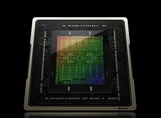
NVIDIA RTX 4090 Doesn't Max-Out AD102, Ample Room Left for Future RTX 4090 Ti

The AD102 silicon on which NVIDIA's new flagship graphics card, the GeForce RTX 4090, is based, is a marvel of semiconductor engineering. Built on the 4 nm EUV (TSMC 4N) silicon fabrication process, the chip has a gargantuan transistor-count of 76.3 billion, a nearly 170% increase over the previous GA102, and a die-size of 608 mm², which is in fact smaller than the 628 mm² die-area of the GA102. This is thanks to TSMC 4N offering nearly thrice the transistor-density of the Samsung 8LPP node on which the GA102 is based.

The AD102 physically features 18,432 CUDA cores, 568 fourth-generation Tensor cores, and 142 third-generation RT cores. The streaming multiprocessors (SM) come with special components that enable the Shader Execution Reordering optimization, which has a significant performance impact on both raster- and ray traced graphics rendering performance. The silicon supports up to 24 GB of GDDR6X or up to 48 GB of GDDR6+ECC memory (the latter will be seen in the RTX Ada professional-visualization card), across a 384-bit wide memory bus. There are 568 TMUs, and a mammoth 192 ROPs on the silicon.

TSMC (Not Intel) Makes the Vast Majority of Logic Tiles on Intel "Meteor Lake" MCM

Intel's next-generation "Meteor Lake" processor is the first mass-production client processor to embody the company's IDM 2.0 manufacturing strategy—one of building processors with multiple logic tiles interconnected with Foveros and a base-tile (essentially an interposer). Each tile is built on a silicon fabrication process most suitable to it, so that the most advanced node could be reserved for the component that benefits from it the most. For example, while you need the SIMD components of the iGPU to be built on an advanced low-power node, you don't need its display controller and media engine to, and these could be relegated to a tile built on a less advanced node. This way Intel is able to maximize its use of wafers for the most advanced nodes in a graded fashion.

Japanese tech publication PC Watch has annotated the "Meteor Lake" SoC, and points out that the vast majority of the chip's tiles and logic die-area is manufactured on TSMC nodes. The MCM consists of four logic tiles—the CPU tile, the Graphics tile, the SoC tile, and the I/O tile. The four sit on a base tile that facilitates extreme-density microscopic wiring interconnecting the logic tiles. The base tile is built on the 22 nm HKMG silicon fabrication node. This tile lacks any logic, and only serves to interconnect the tiles. Intel has an active 22 nm node, and decided it has the right density for the job.

ASML Reports €5.4 Billion Net Sales and €1.4 Billion Net Income in Q2 2022

Today ASML Holding NV (ASML) has published its 2022 second-quarter results. Q2 net sales of €5.4 billion, gross margin of 49.1%, net income of €1.4 billion. Record quarterly net bookings in Q2 of €8.5 billion. ASML expects Q3 2022 net sales between €5.1 billion and €5.4 billion and a gross margin between 49% and 50%. Expected sales growth for the full year of around 10%.

The value of fast shipments*in 2022 leading to delayed revenue recognition into 2023 is expected to increase from around €1 billion to around €2.8 billion.
"Our second-quarter net sales came in at €5.4 billion with a gross margin of 49.1%. Demand from our customers remains very strong, as reflected by record net bookings in the second quarter of €8.5 billion, including €5.4 billion from 0.33 NA and 0.55 NA EUV systems as well as strong DUV bookings.

Samsung Launches Industry's First 24Gbps GDDR6 Memory

Samsung Electronics Co., Ltd., the world leader in advanced memory technology, today announced that it has begun sampling the industry's first 16-gigabit (Gb) Graphics Double Data Rate 6 (GDDR6) DRAM featuring 24-gigabit-per-second (Gbps) processing speeds. Built on Samsung's third-generation 10-nanometer-class (1z) process using extreme ultraviolet (EUV) technology, the new memory is designed to significantly advance the graphics performance for next-generation graphics cards (Video Graphics Arrays), laptops and game consoles, as well as artificial intelligence-based applications and high-performance computing (HPC) systems.

"The explosion of data now being driven by AI and the metaverse is pushing the need for greater graphics capabilities that can process massive data sets simultaneously, at extremely high speeds," said Daniel Lee, executive vice president of the Memory Product Planning Team at Samsung Electronics. "With our industry-first 24 Gbps GDDR6 now sampling, we look forward to validating the graphics DRAM on next-generation GPU platforms to bring it to market in time to meet an onslaught of new demand."

US Wants ASML to Stop Product Shipments to China

ASML is one of the critical semiconductors companies, as they provide tools for making actual silicon. Located in the Netherlands, they are famous for their DUV and EUV lithography tools, used to etch designs onto silicon wafers. According to the report from Bloomberg, the United States governing body is negotiating with the Dutch government to restrict the export of ASML's products to China. This came to affection following US Deputy Commerce Secretary Don Graves's visit to the Netherlands to discuss supply chain issues and meeting with ASML Chief Executive Officer Peter Wennink. While these suggested export restrictions could be beneficial to the strategic placement of US against China, it would hurt ASML's revenue as sales in China accounted for a 16% share of the company's revenue in 2021.

It is recorded that the Chinese spending spree on tools has been the greatest among every country, lasting for two years in a row. By banning ASML from exporting its lithography tools to China, the US could theoretically halt Chinese plans for achieving the government's intended semiconductor independence. The talks with the Dutch government and ASML are still a work in progress, so we are yet to see if the deal is finalized. Additionally, it is worth pointing out that the major US semiconductor manufacturing tool makers like Applied Materials and Lam Research are already banned from exporting to China.

Samsung Begins Chip Production Using 3nm Process Technology With GAA Architecture

Samsung Electronics, the world leader in semiconductor technology, today announced that it has started initial production of its 3-nanometer (nm) process node applying Gate-All-Around (GAA) transistor architecture. Multi-Bridge-Channel FET (MBCFET), Samsung's GAA technology implemented for the first time ever, defies the performance limitations of FinFET, improving power efficiency by reducing the supply voltage level, while also enhancing performance by increasing drive current capability. Samsung is starting the first application of the nanosheet transistor with semiconductor chips for high performance, low power computing application and plans to expand to mobile processors.

"Samsung has grown rapidly as we continue to demonstrate leadership in applying next-generation technologies to manufacturing, such as foundry industry's first High-K Metal Gate, FinFET, as well as EUV. We seek to continue this leadership with the world's first 3 nm process with the MBCFET," said Dr. Siyoung Choi, President and Head of Foundry Business at Samsung Electronics. "We will continue active innovation in competitive technology development and build processes that help expedite achieving maturity of technology."

Intel 4 Process Node Detailed, Doubling Density with 20% Higher Performance

Intel's semiconductors nodes have been quite controversial with the arrival of the 10 nm design. Years in the making, the node got delayed multiple times, and only recently did the general public get the first 10 nm chips. Today, at IEEE's annual VLSI Symposium, we get more details about Intel's upcoming nodes, called Intel 4. Previously referred to as a 7 nm process, Intel 4 is the company's first node to use EUV lithography accompanied by various technologies. The first thing when a new process node is discussed is density. Compared to Intel 7, Intel 4 will double the transistor count for the same area and enable 20% higher performing transistors.

Looking at individual transistor size, the new Intel 4 node represents a very tiny piece of silicon that is even smaller than its predecessor. With a Fin Pitch of 30 nm, Contact Gate Poly Pitch of 50 nm between gates, and Minimum Metal Pitch (M0) of 50 nm, the Intel 4 transistor is significantly smaller compared to the Intel 7 cell, listed in the table below. For scaling, Intel 4 provides double the number of transistors in the same area compared to Intel 7. However, this reasoning is applied only to logic. For SRAM, the new PDK provides 0.77 area reduction, meaning that the same SoC built on Intel 7 will not be half the size of Intel 4, as SRAM plays a significant role in chip design. The Intel 7 HP library can put 80 million transistors on a square millimeter, while Intel 4 HP is capable of 160 million transistors per square millimeter.

Intel "Meteor Lake-P" SoC with 6P+8E Compute Tile Pictured

Intel's next-generation "Meteor Lake-P" mobile processor with a 6P+8E Compute Tile was shown off at the 2022 IEEE VLSI Symposium on Tech and Circuits (6 performance cores and 8 efficiency cores). We now have annotations for all four tiles, as well as a close-up die-shot of the Compute Tile. Intel also confirmed that the Compute Tile will be built on its homebrew Intel 4 silicon fabrication process, which offers over 20% iso-power performance increase versus the Intel 7 node, through extensive use of EUV lithography.

We had earlier seen a 2P+8E version of the "Meteor Lake" Compute Tile, probably from the "Meteor Lake-U" package. The larger 6P+8E Compute tile features six "Redwood Cove" performance cores, and two "Crestmont" efficiency core clusters, each with four E-cores. Assuming the L3 cache slice per P-core or E-core cluster is 2.5 MB, there has to be 20 MB of L3 cache on the compute tile. Each P-core has 2 MB of dedicated L2 cache, while each of the two E-core clusters shares 4 MB of L2 cache among four E-cores.

Micron Moving to EUV Lithography in Taiwan

Although Micron is a predominantly US company, it also has some fabs in Japan, Singapore, the PRC and Taiwan, many of which became part of Micron after it bought other companies. Based on Micron's Computex presentation, it's getting ready to upgrade one of its three fabs in Taichung with extreme ultraviolet (EUV) lithography technology later this year. This is in preparation for the company to move to what it calls its 1-gamma process node for DRAM. Initially this seems to be a R&D node to help the company prepare for a wider rollout of EUV technology. Micron's current DRAM is based on its 1-alpha node and it's planning to move its 1-beta node into volume production next year, in its Taiwan fabs.

Micron's current 1-alpha node is based on DUV technology and was introduced last year, with the company claiming it had a 40 percent improvement in memory density over its previous 1Z node. Micron no longer mentions its die size in the commonly used nanometer measurement, but its 1Z node is said to have been around 11 to 13 nm, so it's likely that the 1-beta node will end up below 10 nm, if its 1-alpha node isn't already below 10 nm. Micron's longer term roadmap also includes a 1-delta node, which was meant to be its first EUV product, but this now seems to have been moved forward to its 1-gamma node. It's likely that Micron will be moving its other fabs to EUV in due time as well, but DRAM has so far not benefitted as much from node shrinks compared to most other types of integrated circuits, so it'll be interesting to see what gains EUV might bring.

Samsung Foundry Considering up to 20 Percent Price Hikes

Earlier this week, news about TSMC increasing prices in 2023 made its way online and now Samsung Foundry is said to be discussing price hikes with its customers to make up for the increased costs in materials. TSMC already increased its prices by around 20 percent at the end of 2021 and now it looks like Samsung Foundry is set to follow suit with a similar price hike. Depending on the node, the company is said to be looking at increases of between 15 to 20 percent. The somewhat peculiar thing in the case of Samsung Foundry, is that the company is looking at asking for more money on older, legacy nodes, than it will for its cutting edge nodes.

The price increases are said to come into effect sometime in the second half of 2022, so more than six months after TSMC's price hike. The company is still in negotiation with some of its customers, while others have already come to an agreement with Samsung Foundries. The costs to produce chips are said to be increasing by 20 to 30 percent across the board, no matter if we're talking materials needed to produce integrated circuits, or building new factories, according to Bloomberg. Samsung Foundries have also managed to secure long-term orders for the next five years, with a combined value of around eight times that of previous year's revenue, according to its EVP, Kang Moon-soo. The company is hoping to overtake TSMC in the future and invested more than US$36 billion in 2021 alone to expand its foundry business with new fabs and EUV machines. The good news is that Samsung Foundry claims to be back on track when it comes to yield on its 4 nm node and mass production of its 3 nm node is said to start this quarter.

ASML Reports Q1 2022 Financial Results

Our first-quarter net sales came in at €3.5 billion which is at the high end of our guidance. The gross margin of 49.0%, is as guided. Our first-quarter net bookings came in at €7.0 billion, including €2.5 billion from 0.33 NA and 0.55 NA EUV systems as well as very strong DUV bookings, reflecting the continued high demand for advanced and mature nodes.

"We continue to see that the demand for our systems is higher than our current production capacity. We accommodate our customers through offering high-productivity upgrades and reducing cycle time in our factories, and we continue to offer a fast shipment process. In addition, we are actively working to significantly expand capacity together with our supply chain partners. In light of the demand and our plans to increase capacity, we expect to revisit our scenarios for 2025 and growth opportunities beyond. We plan to communicate updates in the second half of the year.

TSMC's N3E Node Said to Have Good Yields, Volume Production Expected Q2 2023

Back in March there were reports of TSMC's N3E node having been moved from 2024 to the end of 2023. However, it seems like the node is already seeing better than expected yields and is now being pulled in further and TSMC is expecting to start volume production as early as Q2 in 2023. The node does appear to have been frozen when it comes to further development as of the end of March. Yields are said to be much higher than the N3B node, which is also under development, but with limited information available about it.

The first customer for the new node is expected to be Apple, as the company is largely paying for much of the cutting edge node development at TSMC. However, both Intel and Qualcomm are said to be some of the first customers for the new node. More details should hopefully be announced tomorrow during TSMC's first quarter earnings call. The N3E node is a reduced layer EUV process, but before it goes into mass production, it's likely we'll be seeing the N3 node first. Early production of 3 nm parts later this year is expected to be at around 10 to 20k wafers per month initially, rising to about 25 to 35k a month once TSMC's new fab is ready. Once the N3E node is in full swing, the monthly capacity of 3 nm parts should be around 50k wafers a month, but depending on customer demand, it might end up being even higher.

TSMC Said to be Close to Completing N3E Node

TSMC is working on multiple N3 nodes, with at least N3, N3B and N3E currently being in development. N3 is scheduled for production in 2023, with the N3E node originally being scheduled for 2024, but it now looks like it will be ready ahead of schedule. The N3E node was meant to be an enhanced version of the N3 node, but it now seems to be more of an alternative node, based on fewer EUV layers, supposedly down from 25 to 21 layers, which would make it easier to manufacture. According to details via Morgan Stanley, the N3E node is said to be around eight percent less dense than the original N3 node, but still around 60 percent denser than the N5 node. For comparison, the N3 node was said to have 70 percent denser logic than the N5 node.

The report suggests that the N3E node might be finished by the end of this month, which means production could end up being pulled in by a whole quarter, from Q3'23 to Q2'23. The N3E node is said to "feature improved manufacturing process window with better performance, power and yield", so we might see the N3E node being used for future products by just about anyone that is looking at making high-performance silicon. The N3E node is also said to have higher yields than the N3B node, with N3B said to be an improved version of N3 for certain customers. Not much else is known about the N3B node at the moment.

Intel Updates Technology Roadmap with Data Center Processors and Game Streaming Service

At Intel's 2022 Investor Meeting, Chief Executive Officer Pat Gelsinger and Intel's business leaders outlined key elements of the company's strategy and path for long-term growth. Intel's long-term plans will capitalize on transformative growth during an era of unprecedented demand for semiconductors. Among the presentations, Intel announced product roadmaps across its major business units and key execution milestones, including: Accelerated Computing Systems and Graphics, Intel Foundry Services, Software and Advanced Technology, Network and Edge, Technology Development, More: For more from Intel's Investor Meeting 2022, including the presentations and news, please visit the Intel Newsroom and Intel.com's Investor Meeting site.

Intel Ireland Fab 34 Achieves Development Milestone, Facility to Drive Intel 4 Node

Intel Ireland last week chalked up a milestone in its $7 billion Fab 34 construction project: A team rolled in the new plant's first huge chipmaking tool. The machine, a lithography resist track, arrived by truck at Intel's Leixlip, Ireland, plant after a flight across the Atlantic Ocean from an Intel Oregon plant.

Ireland's new lithography tool runs in conjunction with an extreme ultraviolet (EUV) scanner, a crown jewel in Intel's manufacturing capability. The new tool provides precision coating of silicon wafers before alignment and exposure inside the EUV scanner. The wafer then returns to the lithography tool for a series of precision oven bakes, photo development and rinsing. A typical Intel fab contains about 1,200 advanced tools, many of them costing millions of dollars a piece.

Intel Purchases ASML TWINSCAN EXE:5200 EUV Production System

Today, ASML Holding and Intel Corporation announced the latest phase of their longstanding collaboration to advance the cutting edge of semiconductor lithography technology. Intel has issued its first purchase order to ASML for the delivery of the industry's first TWINSCAN EXE:5200 system - an extreme ultraviolet (EUV) high-volume production system with a high numerical aperture and more than 200 wafers per hour productivity - as part of the two companies' long-term High-NA collaboration framework.

"Intel's vision and early commitment to ASML's High-NA EUV technology is proof of its relentless pursuit of Moore's Law. Compared to the current EUV systems, our innovative extended EUV roadmap delivers continued lithographic improvements at reduced complexity, cost, cycle time and energy that the chip industry needs to drive affordable scaling well into the next decade," said ASML President and CTO Martin van den Brink.

Samsung Introduces Game Changing Exynos 2200 Processor with Xclipse GPU Powered by AMD RDNA2 Architecture

Samsung Electronics Co., Ltd., a world leader in advanced semiconductor technology, today announced its new premium mobile processor, the Exynos 2200. The Exynos 2200 is a freshly designed mobile processor with a powerful AMD RDNA 2 architecture based Samsung Xclipse graphics processing unit (GPU). With the most cutting-edge Arm -based CPU cores available in the market today and an upgraded neural processing unit (NPU), the Exynos 2200 will enable the ultimate mobile phone gaming experience, as well as enhancing the overall experience in social media apps and photography.

"Built on the most advanced 4-nanometer (nm) EUV (extreme ultraviolet lithography) process, and combined with cutting-edge mobile, GPU, and NPU technology, Samsung has crafted the Exynos 2200 to provide the finest experience for smartphone users. With the Xclipse, our new mobile GPU built with RDNA 2 graphics technology from the industry leader AMD, the Exynos 2200 will redefine mobile gaming experience, aided by enhanced graphics and AI performance," said Yongin Park, President of System LSI Business at Samsung Electronics. "As well as bringing the best mobile experience to the users, Samsung will continue its efforts to lead the journey in logic chip innovation."

ASML Provides Damage Assessment of Fire Incident, EUV Component Production Affected

ASML, makers of vital semiconductor fabrication machinery powering the world's leading fabs, including TSMC, provided its first damage-assessment of the fire incident at one of its component plants near Berlin, on January 3. This plant manufactures several mechanical and optical components of semiconductor fabrication machinery, such as wafer tables and clamps, reticle chucks and mirror blocks.

ASML, in a press-release, disclosed that production of components used in DUV (deep-ultraviolet) machines, has been restarted, as that area of the plant is unaffected by the fire. A region of the plant that manufactures wafer clamps for use in its EUV (extreme ultraviolet) machines, however, has been affected by the fire. The company is still in the process of coming up with a recovery plan for this area, and will come up with a tentative date for restart of production only after that. EUV lithography is leveraged for 5 nm and upcoming 3 nm silicon fabrication nodes at TSMC, Samsung, and Intel. TSMC is known to be ASML's largest customer. ASML stated that it will release its Q4-2021 and full-year 2021 financial results on January 19, and it may provide more updates on the matter.
The press-release follows.

SK hynix Becomes the Industry's First to Ship 24Gb DDR5 Samples

SK hynix today announced that it has shipped samples of 24 Gigabit (Gb) DDR5* DRAM with the industry's largest density for a single DRAM chip. The announcement of SK hynix releasing the industry's largest density DDR5 chip comes in just 14 months after the Company became the first to release DDR5 DRAM in October 2020, further solidifying the chipmaker's technological leadership in DDR5.

The new 24 Gb DDR5 was produced with the cutting-edge 1 anm technology that utilizes EUV process. It has a density of 24Gb per chip, which is up from the existing density of 16 Gb in 1 ynm DDR5, with improved production efficiency and increased speed by up to 33%. In addition, SK hynix managed to reduce the product's power consumption by *25% compared to existing products while lowering energy use in manufacturing through enhanced production efficiency. SK hynix expects the product to bring about reduction in carbon emissions as well, which is meaningful in the context of ESG management.

TSMC 3 nm To Enter Volume Production in 2022

TSMC will commercialize its N3 (3 nm) EUV silicon fabrication node in 2022, with volume production set to commence in the second half of the year. The company is looking to maximize capacity on its current N5 (5 nm) node, which already serves major customers such as Apple. AMD is expected to utilize N5 allocation going into 2022 as its next-generation "Zen 4" processors are expected to leverage the node to drive up CPU core counts and caches. The company is also utilizing N6 (6 nm) for its CDNA2 compute accelerator logic dies. N5 could also power mobile application processors from several manufacturers.

Annual DRAM Revenue for 2022 Expected to Reach US$91.5 Billion, with Prices Likely to Rally in 2H22, Says TrendForce

Despite the forecasted 18.6% YoY growth in total DRAM bit supply next year, the global DRAM market is still expected to shift from a shortage situation to an oversupply, according to TrendForce's latest investigations. This shift can primarily be attributed to the fact that, not only are most buyers now carrying a relatively high level of DRAM inventory, but DRAM bit demand is also expected to increase by only 17.1% YoY in 2022. On the price front, the oversupply situation will result in a drop in DRAM ASP in 2022 but not a major decline in annual DRAM revenue, thanks to the oligopolistic nature of the DRAM industry. Annual DRAM revenue for 2022 is expected to reach US$91.54 billion, which represents a slight YoY increase of 0.3%.

Based on an analysis of DRAM sufficiency ratio (which refers to the surplus of supply in comparison with demand) for each quarter in 2022, TrendForce forecasts a 15% YoY decrease in DRAM ASP for 2022, with prices undergoing the more noticeable declines during the first half of the year. Heading into 2H22, however, owing to the rise in DDR5 penetration rate, as well as the arrival of peak seasonal demand, the decline in DRAM ASP will likely narrow. TrendForce does not rule out the possibility that DRAM ASP may even hold flat or undergo an increase in 2H22.

ASML Reports €5.2 Billion Net Sales and €1.7 Billion Net Income in Q3 2021

Today, ASML Holding NV (ASML) has published its 2021 third-quarter results. "Our third-quarter net sales came in at €5.2 billion with a gross margin of 51.7%, both within our guidance. Our third-quarter net bookings came in at €6.2 billion, including €2.9 billion from EUV systems. The demand continues to be high. The ongoing digital transformation and current chip shortage fuel the need to increase our capacity to meet the current and expected future demand for Memory and for all Logic nodes. ASML expects fourth-quarter net sales between €4.9 billion and €5.2 billion with a gross margin between 51% and 52%. ASML expects R&D costs of around €670 million and SG&A costs of around €195 million. For the full year, we are on track to achieving growth approaching 35%," said ASML President and Chief Executive Officer Peter Wennink.

Samsung Starts Mass Production of Most Advanced 14 nm EUV DDR5 DRAM

Samsung Electronics, the world leader in advanced memory technology, today announced that it has begun mass producing the industry's smallest, 14-nanometer (nm), DRAM based on extreme ultraviolet (EUV) technology. Following the company's shipment of the industry-first EUV DRAM in March of last year, Samsung has increased the number of EUV layers to five to deliver today's finest, most advanced DRAM process for its DDR5 solutions.

"We have led the DRAM market for nearly three decades by pioneering key patterning technology innovations," said Jooyoung Lee, Senior Vice President and Head of DRAM Product & Technology at Samsung Electronics. "Today, Samsung is setting another technology milestone with multi-layer EUV that has enabled extreme miniaturization at 14 nm—a feat not possible with the conventional argon fluoride (ArF) process. Building on this advancement, we will continue to provide the most differentiated memory solutions by fully addressing the need for greater performance and capacity in the data-driven world of 5G, AI and the metaverse."

Samsung Confirms RDNA2-based Exynos 2200 iGPU Will Support Ray Tracing

Samsung appears to be in a hurry to beat Apple and Qualcomm at bringing real-time ray tracing to the smartphone space, with its next-generation Exynos 2200 "Pamir" SoC. The chip integrates a graphics processor based on the AMD RDNA2 architecture, codenamed "Voyager." Samsung all but confirmed that the compute units of this will feature Ray Accelerators, the hardware component that performs ray-intersection calculations. The "Voyager" iGPU, as implemented on the Exynos 2200 SoC, physically features six RDNA2 compute units (384 stream processors), and hence six Ray Accelerators.

Built on the 4 nm EUV silicon fabrication process, Exynos 2200 will feature not two, but three kinds of CPU cores—four lightweight efficiency cores, three mid-tier cores, and one ultra high-performance core. Each of these three operate in unique performance/Watt bands, giving software finer-grained control over the kinds of hardware resources they want. Samsung is expected to debut the Exynos 2200 with its next-generation Galaxy S and Galaxy Note devices.

Fabricating the Fabs: ASML Vision Document Predicts 300 Billion-Transistor Logic by 2030

"Moore's Law is alive and well," says ASML, in its vision document addressing investors. The company manufactures the machines that perform the actual task of silicon lithography—turning silicon discs into wafers of logic or storage chips. It highlighted the various technologies making progress, which will help its semiconductor-fabrication customers, such as TSMC and their hundreds of clients, sustain Moore's Law all the way through this decade. The company predicts SoCs with as many as 300 billion transistors by 2030. To achieve this, the company is innovating in two distinct directions—at the chip-level, to increase transistor density per chip to over 50 billion transistors; and at the system level, through packaging technology innovations, to reach that ultimate transistor count.

According to ASML's roadmap, at the turn of the decade, its technology enables 5 nm-class in production, and is at the cusp of a major breakthrough, nanosheet-FETs. which pave the way for 3 nm and 2 nm nodes, backed by EUV lithography. The journey from 2 nm to 1.5 nm will require another breakthrough, forked-nanosheets, and from 1.5 nm to 1 nm yet another breakthrough, CFET. Sub-1 nm fabrication will be possible toward the turn of this decade, thanks to 2D atomic channel technology, which is how chip-designers will be able to cram over 50 billion transistors per chip, and build MCM systems with over 300 billion transistors. The presentation predicts that besides 3D packaging, stacked silicon will also play a role, with multiple stacked logic layers, heterogenous chips with logic, storage, and I/O layers, stacked DRAM (up from single-digit layers to double-digits; and for NAND flash to grow from the current 176-layer, to nearly 500-layer by 2030.
Return to Keyword Browsing
Jul 15th, 2025 16:12 CDT change timezone

New Forum Posts

Popular Reviews

TPU on YouTube

Controversial News Posts