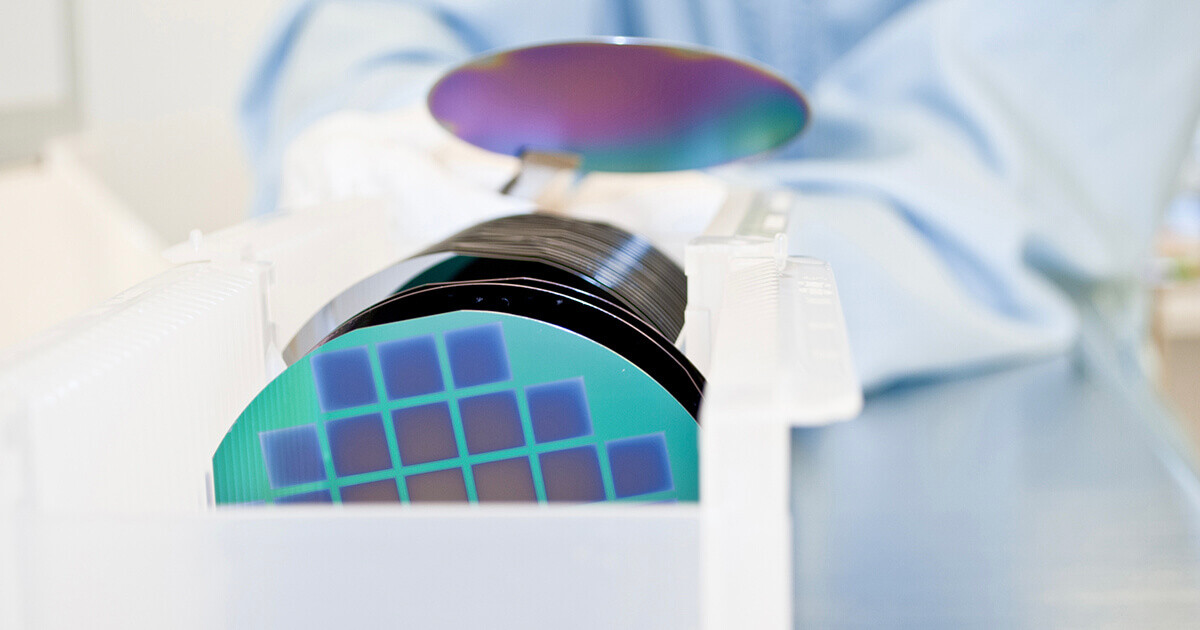
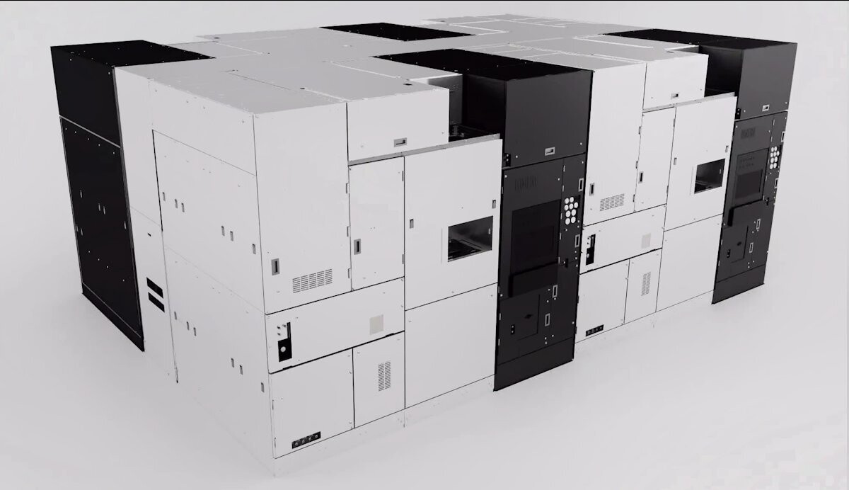
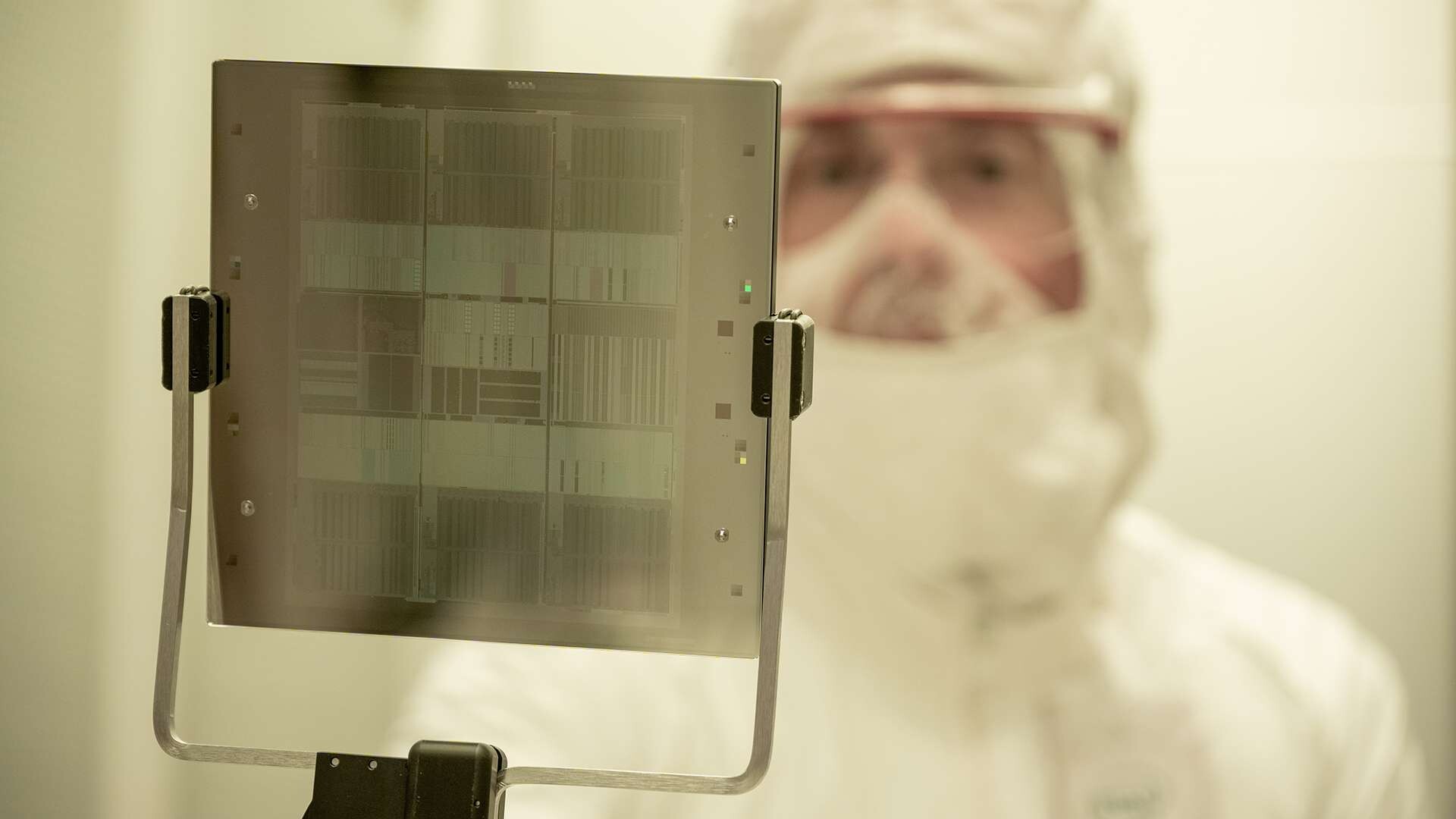
ASML Celebrates First Installation of Twinscan NXE:3800E Low-NA EUV Litho Tool
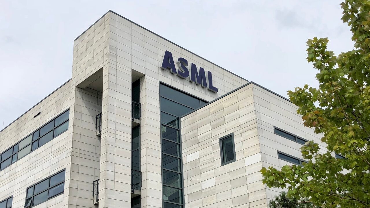
ASML celebrated an important milestone last week—the company's social media account shared news about their third generation extreme ultraviolet (EUV) lithography tool reaching an unnamed customer: "chipmakers have a need for speed! The first Twinscan NXE:3800E is now being installed in a chip fab. 🔧 With its new wafer stages, the system will deliver leading edge productivity for printing advanced chips. We're pushing lithography to new limits." The post included a couple of snaps—ASML workers were gathered in front of a pair of climatized containers, and Peter Wennink (President and CEO) and Christophe Fouquet (EVP and CBO) thanked staff at company HQ.
The Twinscan NXE:3800E is ASML's latest platform from a series of 0.33 numerical aperture (Low-NA) lithography scanners. Information is scarce—the company has not yet published a 3800E product page. The preceding model—Twinscan NXE:3600D—supports EUV volume production at 3 and 5 nm. ASML roadmaps imply that the Twinscan NXE:3800E has been designed to produce chips on 2 and 3 nm-class technologies. The company's cutting-edge High-NA extreme ultraviolet (EUV) chipmaking tools (High-NA Twinscan EXE) are expected to cost around $380 million—reports from last month point to a possible $183 million price point for "existing Low-NA EUV lithography systems." Another Low-NA EUV machine is reported to be lined up for a possible 2026 release window—ASML's next-gen Twinscan NXE:4000F model will co-exist alongside emerging (pricier) High-NA solutions.


The Twinscan NXE:3800E is ASML's latest platform from a series of 0.33 numerical aperture (Low-NA) lithography scanners. Information is scarce—the company has not yet published a 3800E product page. The preceding model—Twinscan NXE:3600D—supports EUV volume production at 3 and 5 nm. ASML roadmaps imply that the Twinscan NXE:3800E has been designed to produce chips on 2 and 3 nm-class technologies. The company's cutting-edge High-NA extreme ultraviolet (EUV) chipmaking tools (High-NA Twinscan EXE) are expected to cost around $380 million—reports from last month point to a possible $183 million price point for "existing Low-NA EUV lithography systems." Another Low-NA EUV machine is reported to be lined up for a possible 2026 release window—ASML's next-gen Twinscan NXE:4000F model will co-exist alongside emerging (pricier) High-NA solutions.