News Posts matching #Foundry

Return to Keyword Browsing

Samsung Electronics Announces Second Quarter 2021 Results

Samsung Electronics today reported financial results for the second quarter ended June 30, 2021. Total consolidated revenue was KRW 63.67 trillion, a 20% increase from the previous year and a record for the second quarter. Operating profit increased 34% from the previous quarter to KRW 12.57 trillion as market conditions improved in the memory market, operations normalized at the Austin foundry fab, and as effective global supply chain management (SCM) helped maintain solid profitability for the finished product businesses.

The Semiconductor business saw a significant improvement in earnings as memory shipments exceeded previous guidance and price increases were higher than expected, while the Company strengthened its cost competitiveness. For the Display Panel Business, a one-off gain and an increase in overall prices boosted profits.

Samsung Announces Availability of Its Next Generation 2.5D Integration Solution I-Cube4 for High-Performance Applications

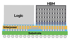
Samsung Electronics Co., Ltd., a world leader in advanced semiconductor technology, today announced the immediate availability of its next-generation 2.5D packaging technology Interposer-Cube4 (I-Cube4), leading the evolution of chip packaging technology once again. Samsung's I-CubeTM is a heterogeneous integration technology that horizontally places one or more logic dies (CPU, GPU, etc.) and several High Bandwidth Memory (HBM) dies on top of a silicon interposer, making multiple dies operate as a single chip in one package.

Samsung's new I-Cube4, which incorporates four HBMs and one logic die, was developed in March as the successor of I-Cube2. From high-performance computing (HPC) to AI, 5G, cloud and large data center applications, I-Cube4 is expected to bring another level of fast communication and power efficiency between logic and memory through heterogeneous integration.

Samsung Demonstrates 256 Gb 3 nm MBCFET Chip at ISSCC 2021

During the IEEE International Solid-State Circuits Conference (ISSCC), Samsung Foundry has presented a new step towards smaller and more efficient nodes. The new chip that was presented is a 256 Gb memory chip, based on SRAM technology. However, all of that doesn't sound interesting, until we mention the technology that is behind it. Samsung has for the first time manufactured a chip using the company's gate-all-around field-effect transistor (GAAFET) technology on the 3 nm semiconductor node. Formally, there are two types of GAAFET technology: the regular GAAFET that uses nanowires as fins of the transistor, and MBCFET (multi-bridge channel FET) that uses thicker fins that come in a form of a nanosheet.

Samsung has demonstrated the first SRAM chip that uses MBCFET technology today. The chip in question is a 256 Gb chip with an area of 56 mm². The achievement Samsung is proud of is that the chip uses 230 mV less power for writes, compared to the standard approach, as the MBCFET transistors allow the company to have many different power-saving techniques. The new 3 nm MBCFET process is expected to get into high-volume production sometime in 2022, however, we are yet to see demos of logic chips besides SRAM like we see today. Nonetheless, even the demonstration of SRAM is big progress, and we are eager to see what the company manages to build with the new technology.

Prices of NAND Flash Controller ICs Poised to Rise by 15-20% due to Tightening Production Capacity for Foundry Services, Says TrendForce

In the upstream semiconductor industry, the major foundries such as TSMC and UMC are reporting fully loaded capacities, while in the downstream, the available production capacity for OSAT is also lacking, according to TrendForce's latest investigations. Given this situation, suppliers of NAND Flash controller ICs such as Phison and Silicon Motion are now unable to meet upside demand from their clients. Not only have many controller IC suppliers temporarily stopped offering quotes for new orders, but they are also even considering raising prices soon because the negotiations between NAND Flash suppliers and module houses over 1Q21 contracts are now at the critical juncture. The potential increases in prices of controller ICs from outsourced suppliers (IC design houses) are currently estimated to be the range of 15-20%.

With regards to the demand side, demand has risen significantly for eMMC solutions with medium- and low-density specifications (i.e., 64 GB and lower), for which NAND Flash suppliers have mostly stopped updating the NAND Flash process technology, while maintaining support with the legacy 2D NAND or the 64L 3D NAND process. This is on account of strong sales for Chromebook devices and TVs. As older processes gradually account for a lowering portion of bit output proportions from NAND Flash suppliers, these companies are exhibiting a lowered willingness to directly supply such eMMC products to clients. As a result, clients now need to turn to memory module houses, which are able to source NAND Flash components and controllers, to procure eMMC products in substantial quantities.

TSMC Approves 3.5 Billion Dollar Arizona Foundry

TSMC plans to open a new 3.5 billion dollar foundry in Arizona with a new wholly-owned US subsidiary. The new foundry will begin construction in 2021 with an expected completion date of 2024. The new facility will target production volumes of 20,000 wafers per month with 5 nm production being the main priority. TSMC will be joining Intel who also produces chips in Arizona enabling them to tap into this well-established supply chain. TSMC plans to employ 1,600 staff at the facility which will be their most advanced facility outside of Taiwan. The new foundry will likely be popular with US customers and military applications requiring more secure facilities.

Raja Koduri to Present at Samsung Foundry Forum amid Intel's Outsourcing Efforts

Intel's chief architect and senior vice president of discrete graphics division, Mr. Raja Koduri, is said to be scheduled to present at Samsung Electronics Event day. With a presentation titled "1000X More Compute for AI by 2025", the event is called Samsung Foundry SAFE Forum. It is a global virtual conference designed to be available to everyone. So you might be wondering what is Mr. Koduri doing there. Unless you have been living under a rock, you know about Intel's struggles with node manufacturing. Specifically, the 10 nm node delays that show the company's efforts to deliver a node on time. The same is happening with the 7 nm node that also experienced significant delays.

Intel has a contract to develop an exascale supercomputer at Argonne National Laboratory, called Aurora. That supercomputer is using Intel's CPUs and the company's upcoming Xe GPUs. Since the company has problems with manufacturing and has to deliver the products (it is bound by several contracts) to its contractors and customers, it decided to look at external manufacturers for its products, specifically Xe graphics. Being that Mr. Koduri tweeted an image of him visiting Samsung Giheung Fab in Korea, and now presenting at the Samsung Foundry event, it is possible that Intel will tap Samsung's semiconductor manufacturing process for its Xe GPU efforts and that Samsung will be the contractor in charge.

China Forecast to Represent 22% of the Foundry Market in 2020, says IC Insights

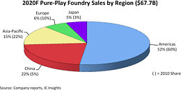
IC Insights recently released its September Update to the 2020 McClean Report that presented the second of a two-part analysis on the global IC foundry industry and included a look at the pure-play foundry market by region.

China was responsible for essentially all of the total pure-play foundry market increase in 2018. In 2019, the U.S./China trade war slowed China's economic growth but its foundry marketshare still increased by two percentage points to 21%. Moreover, despite the Covid-19 shutdown of China's economy earlier this year, China's share of the pure-play foundry market is forecast to be 22% in 2020, 17 percentage points greater than it registered in 2010 (Figure 1).

COVID-19 Drives Rise in Global Fab Equipment Spending, SEMI Reports

Soaring pandemic-inspired demand for chips that power everything from communications and IT infrastructures to personal computing, gaming and healthcare electronics will drive an 8% increase in global fab equipment spending in 2020 and a 13% increase in 2021, SEMI announced today in its World Fab Forecast report. Rising demand for semiconductors for datacenter infrastructures and server storage along with the buildup of safety stock as U.S.-China trade tensions intensify are also contributing to this year's growth.

The bullish trend for overall fab equipment investments comes as the semiconductor industry recovers from a 9% decline in fab spending in 2019 and navigates a roller-coaster 2020 with actual and projected spending drops in the first and third quarters mixed with second- and fourth-quarter increases. See figure below:

Samsung Announces Availability of its Silicon-Proven 3D IC Technology

Samsung Electronics Co., Ltd., a world leader in advanced semiconductor technology, today announced the immediate availability of its silicon-proven 3D IC packaging technology, eXtended-Cube (X-Cube), for today's most advanced process nodes. Leveraging Samsung's through-silicon via (TSV) technology, X-Cube enables significant leaps in speed and power efficiency to help address the rigorous performance demands of next-generation applications including 5G, artificial intelligence, high-performance computing, as well as mobile and wearable.

"Samsung's new 3D integration technology ensures reliable TSV interconnections even at the cutting-edge EUV process nodes," said Moonsoo Kang, senior vice president of Foundry Market Strategy at Samsung Electronics. "We are committed to bringing more 3D IC innovation that can push the boundaries of semiconductors."

SMIC 7nm-class N+1 Foundry Node Going Live by Q4-2020

China's state-backed SMIC (Semiconductor Manufacturing International Corporation) has set an ambitious target of Q4-2020 for its 7 nanometer-class N+1 foundry node to go live, achieving "small scale production," according to a cnTechPost report. The company has a lot of weight on its shoulders as geopolitical hostility between the U.S. and China threatens to derail the country's plans to dominate 5G technology markets around the world. The SMIC N+1 node is designed to improve performance by 20%, reduce chip power consumption by 57%, reduce logic area by 63%, and reduce SoC area by 55%, in comparison to the SMIC's 14 nm FinFET node, Chinese press reports citing a statement from SMIC's co-CEO Dr. Liang Mengsong.

Dr. Liang confirmed that the N+1 7 nm node and its immediate successor will not use EUV lithography. N+1 will receive a refinement in the form of N+2, with modest chip power consumption improvement goals compared to N+1. This is similar to SMIC's 12 nm FinFET node being a refinement of its 14 nm FinFET node. Later down its lifecycle, once the company has got a handle of its EUV lithography equipment, N+2 could receive various photomasks, including a switch to EUV at scale.

Samsung Successfully Completes 5nm EUV Development

Samsung Electronics Co., Ltd., a world leader in advanced semiconductor technology, today announced that its 5-nanometer (nm) FinFET process technology is complete in its development and is now ready for customers' samples. By adding another cutting-edge node to its extreme ultraviolet (EUV)-based process offerings, Samsung is proving once again its leadership in the advanced foundry market.

Compared to 7 nm, Samsung's 5 nm FinFET process technology provides up to a 25 percent increase in logic area efficiency with 20 percent lower power consumption or 10 percent higher performance as a result of process improvement to enable us to have more innovative standard cell architecture. In addition to power performance area (PPA) improvements from 7 nm to 5 nm, customers can fully leverage Samsung's highly sophisticated EUV technology. Like its predecessor, 5 nm uses EUV lithography in metal layer patterning and reduces mask layers while providing better fidelity.

Samsung Completes Qualification of 8 nm LPP Process

Samsung Electronics announced today that their 8 nm FinFET process technology, 8LPP (Low Power Plus), has been qualified and is ready for production. Samsung's newest process node provides up to 10-percent lower power consumption with up to 10-percent area reduction from 10LPP through a narrower metal pitch. 8LPP is expected to provide benefits for applications including mobile, cryptocurrency and network/server. Samsung expects this 8 nm node to be the last feasible one with current fabrication technology - shown by the fact it's actually employing much of the same design and production processes and philosophy as the 10 nm node. Samsung is counting on EUV (Extreme Ultra Violet) technology to enable 7 nm and smaller process nodes.

"With the qualification completed three months ahead of schedule, we have commenced 8LPP production," said Ryan Lee, Vice President of Foundry Marketing at Samsung Electronics. "Samsung Foundry continues to expand its process portfolio in order to provide distinct competitive advantages and excellent manufacturability based on what our customers and the market require." Details of the recent update to Samsung's foundry roadmap, including 8LPP availability and 7nm EUV development, will be presented at the Samsung Foundry Forum Europe on October 18, 2017, in Munich, Germany.

Samsung Announces 11nm LPP and 7nm LPP With EUV Technology

Samsung Electronics Co., Ltd., the world leader in advanced semiconductor technology, today announced it has added 11-nanometer (nm) FinFET process technology (11LPP, Low Power Plus) to its advanced foundry process portfolio, offering customers with an even wider range of options for their next-generation products. Through further scaling from the earlier 14LPP process, 11LPP delivers up to 15 percent higher performance and up to 10 percent chip area reduction with the same power consumption.

In addition to the 10nm FinFET process for mobile processors in premium flagship smartphones, the company expects its 11nm process to bring differentiated value to mid- to high-end smartphones. The new process technology is scheduled to be ready for production in the first half of 2018. Samsung also confirmed that development of 7LPP with EUV (extreme ultra violet) lithography technology is on schedule, targeting its initial production in the second half of 2018.

Since 2014, Samsung has processed close to 200,000 wafers with EUV lithography technology and, building on its experience, has recently seen visible results in process development such as achieving 80 percent yield for 256 megabit (Mb) SRAM (static random-access memory).

Samsung Completes Qualification of its 2nd Generation 10nm Process Technology

Samsung Electronics Co., Ltd., a world leader in advanced semiconductor technology, announced today that its second generation 10-nanometer (nm) FinFET process technology, 10LPP (Low Power Plus), has been qualified and is ready for production. With further enhancement in 3D FinFET structure, 10LPP allows up to 10-percent higher performance or 15-percent lower power consumption compared to the first generation 10LPE (Low-Power Early) process with the same area scaling.

Samsung was the first in the industry to begin mass production of system-on-chips (SoCs) products on 10LPE last October. The latest Samsung Galaxy S8 smartphones are powered by some of these SoCs. To meet long-term demand for the 10nm process for a wide range of customers, Samsung has started installing production equipment at its newest S3-line in Hwaseong, Korea. The S3-line is expected to be ready for production by the fourth quarter of this year.

Samsung Details New Foundry Offerings at 14nm (LPU) and 10nm (LPU)

In an announcement that's sure to stir the foundry gods, Samsung Electronics, a world leader in advanced semiconductor technology, announced today that it is expanding its advanced foundry process technology offerings with the fourth-generation 14-nanometer (nm) process (14LPU) and the third-generation 10nm process (10LPU). The announcement comes as Samsung increases investment so as to meet the requirements of next generation products, ranging from mobile and consumer electronics (Snapdragon 830 and Samsung's own Exynos 8895 come to mind) to data centers and automotives.

Ben Suh, Senior Vice President of foundry marketing at Samsung Electronics, issued the following statement: "After we announced the industry's first 10nm mass production in mid-October, we have now also expanded our lineup with new foundry offerings, 14LPU and 10LPU. Samsung is very confident with our technology definitions that provide design advantages on an aggressive process with manufacturability considerations. We have received tremendous positive market feedback and are looking forward to expanding our leadership in the advanced process technology space."
Return to Keyword Browsing
Apr 6th, 2025 20:55 EDT change timezone

New Forum Posts

Popular Reviews

Controversial News Posts