Apr 18th, 2025 15:46 EDT
change timezone
Latest GPU Drivers
New Forum Posts
- Place your bets, what node will rtx 6000/RDNA 5(UDNA 1?) use (8)
- Can Intel recover in DYI market anytime soon? (10)
- TPU's Nostalgic Hardware Club (20257)
- GPU Pricing and Performance (15)
- What are you playing? (23396)
- Spoofer Modified SMBIOS/BIOS – Need Help Restoring Original Motherboard Info (TUF GAMING B550-PLUS WiFi II) (2)
- Tried installing 576.02 - installer window disappears (20)
- RX 9000 series GPU Owners Club (392)
- GPU Database (300)
- Drives fail to work with Rufus Windows TO GO (2)
Popular Reviews
- ASUS GeForce RTX 5060 Ti TUF OC 16 GB Review
- NVIDIA GeForce RTX 5060 Ti PCI-Express x8 Scaling
- Palit GeForce RTX 5060 Ti Infinity 3 16 GB Review
- G.SKILL Trident Z5 NEO RGB DDR5-6000 32 GB CL26 Review - AMD EXPO
- ASUS GeForce RTX 5060 Ti Prime OC 16 GB Review
- Teevolution Terra Pro Review
- MSI GeForce RTX 5060 Ti Gaming OC 16 GB Review
- Zotac GeForce RTX 5060 Ti AMP 16 GB Review
- MSI GeForce RTX 5060 Ti Gaming Trio OC 16 GB Review
- ASUS GeForce RTX 5080 TUF OC Review
Controversial News Posts
- NVIDIA GeForce RTX 5060 Ti 16 GB SKU Likely Launching at $499, According to Supply Chain Leak (182)
- NVIDIA Sends MSRP Numbers to Partners: GeForce RTX 5060 Ti 8 GB at $379, RTX 5060 Ti 16 GB at $429 (127)
- Nintendo Confirms That Switch 2 Joy-Cons Will Not Utilize Hall Effect Stick Technology (105)
- Over 200,000 Sold Radeon RX 9070 and RX 9070 XT GPUs? AMD Says No Number was Given (100)
- NVIDIA Launches GeForce RTX 5060 Series, Beginning with RTX 5060 Ti This Week (100)
- Nintendo Switch 2 Launches June 5 at $449.99 with New Hardware and Games (99)
- Sony Increases the PS5 Pricing in EMEA and ANZ by Around 25 Percent (85)
- NVIDIA PhysX and Flow Made Fully Open-Source (77)
News Posts matching #G200
Return to Keyword Browsing
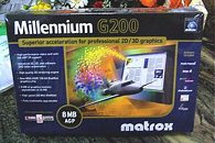
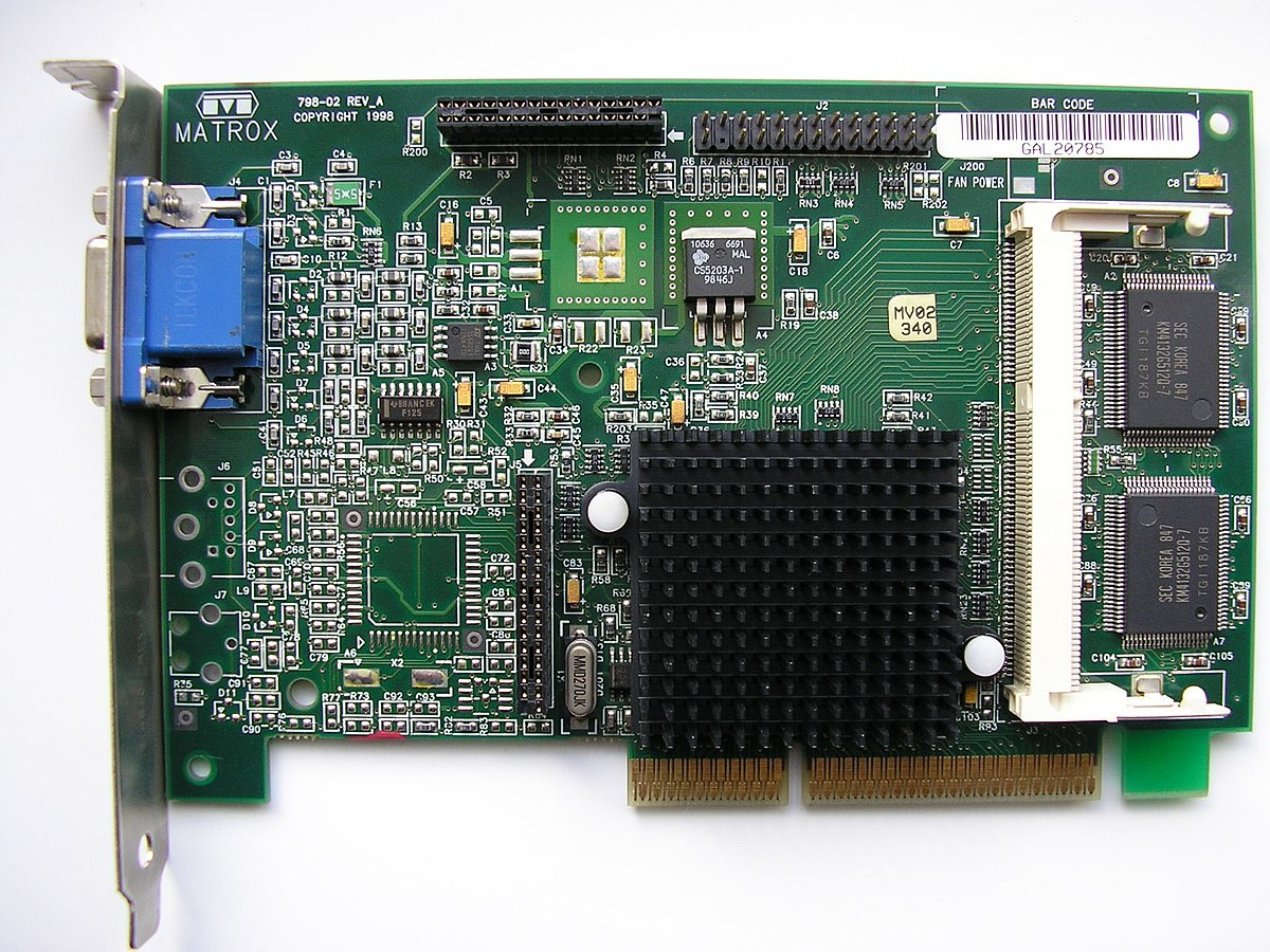
Matrox G200 - Celebrating 20 Years of Graphics Excellence
Matrox Graphics Inc. is pleased to announce the 20-year anniversary of its Matrox G200 graphics chip. The milestone celebrates two decades of dedicated, active software development and support for multiple technology nodes across countless Microsoft Windows and Linux operating systems. Developed for 2D, 3D, and video acceleration, the G200 powered a number of industry-first, graphics and multi-monitor-based product lines that delivered unprecedented image quality across one or more displays. Today, G200 is and remains the trusted and preeminent integrated graphics solution of choice for the majority of baseboard management controllers used in servers worldwide.


Akasa Readies Freedom Force Universal VGA Cooler
Akasa is readying a new graphics card cooler for the consumer segment, this time touting support for almost all current single-GPU graphics cards. The Akasa Freedom Force was first pictured at the CeBIT event. It measures 190(L) x 107.5(W) x 55(H), and weighs in at 440 g. Its design consists of a GPU contact block that doubles up as a heatsink, from which four aluminum heatpipes convey heat to two aluminum fin blocks on either side of the GPU block. Each block is subject to air-flow by its own white LED-lit fan that spins at 2200 rpm. The GPU block has mount holes for 43.2 mm, 53.2 mm, and 61.5 mm cooler mounts. Also bundled are nine memory chip heatsinks. The cooler supports one of the broadest range of GPUs, including NVIDIA GeForce GTX 200 (GTX 260, 275, 280, 285), ATI Radeon HD 4000/3000/2000, GeForce 9/8/7 series, etc. A word of caution however, would be that the cooler doesn't pack VRM heatsinks, or heatsinks for NVIO display processors featured on G200(b) and G80 based graphics cards. It will reach retail in about a month's time, and is expected to be priced at 30 EUR (US $40.5).


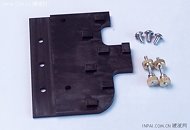
Dongwon Innovates Modular Full-Coverage G200 Series Water-Block
Relatively unknown to the west, yet popular in the Asian OEM and retail markets, Chinese component cooler designer Dongwon has innovated a modular full-coverage design for its water-block which boosts its compatibility. The block serves as a simple answer to NVIDIA's almost ever-changing reference PCB design for its single-GPU GeForce GTX 200 series accelerators. The design allows this water-block to fit the P651 (65 nm GeForce GTX 260 and GTX 280), P654 (first versions of 55 nm GeForce GTX 260 and GTX 285), and the newer P897 PCB design for the 55 nm cards.
The full-coverage block consists of two segments: the main unit which provides coverage for the GPU, the memory and the NVIO2 processor; and the second segment that covers the VRM area. The segment's grooves are designed to cover the LFPAK VRM arrangement on P651 and P654, while it can be detached to allow the rest of the block to be used on the P897. We're not entirely sure if the design concept circled around compatibility with different PCB designs, though it ends up being the block's most useful application. Although the company has seemingly no presence in the western retail channels, one can expect this block to come factory-fitted on graphics cards.


The full-coverage block consists of two segments: the main unit which provides coverage for the GPU, the memory and the NVIO2 processor; and the second segment that covers the VRM area. The segment's grooves are designed to cover the LFPAK VRM arrangement on P651 and P654, while it can be detached to allow the rest of the block to be used on the P897. We're not entirely sure if the design concept circled around compatibility with different PCB designs, though it ends up being the block's most useful application. Although the company has seemingly no presence in the western retail channels, one can expect this block to come factory-fitted on graphics cards.


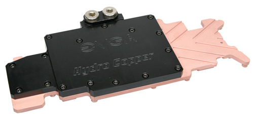
EVGA GeForce GTX 285 Water Block Pictured
NVIDIA's 55nm GeForce GTX 200 series cards seem to be doing well at the markets. Cashing in on their success, EVGA plans to release GeForce GTX 285 and GTX 295 accelerators which are ready for water-cooling. While not much is known about the specifics of water cooling the GTX 295 part comes with, the GTX 285 SKU comes in the form of cards with factory-fitted water blocks.
NVIDIA made several changes to the PCB of its single-GPU G200 PCB, making GeForce GTX 280 water blocks incompatible with the GTX 285 PCB. The new PCB has a rearranged memory layout, with all its memory chips positioned on the business-area of the PCB, and a re-arranged VRM area. The new EVGA Hydro Copper block is designed to be a monolithic full-coverage block with a copper base. The SKU most likely to be carved out using this block could be the EVGA e-GeForce GTX 285 Hydro Copper. The company could take advantage of this superior cooling to set extremely high factory-overclocked parameters to the GPU and memory. This is the same company that released the GeForce GTX 285 FTW with audacious clock speeds of 720/1,620/2,772 MHz (core/shader/memory) using the NVIDIA reference design cooler. As with all water block-fitted graphics cards from EVGA in the past, the company could charge a premium over all its air-cooled GeForce GTX 285 models.
NVIDIA made several changes to the PCB of its single-GPU G200 PCB, making GeForce GTX 280 water blocks incompatible with the GTX 285 PCB. The new PCB has a rearranged memory layout, with all its memory chips positioned on the business-area of the PCB, and a re-arranged VRM area. The new EVGA Hydro Copper block is designed to be a monolithic full-coverage block with a copper base. The SKU most likely to be carved out using this block could be the EVGA e-GeForce GTX 285 Hydro Copper. The company could take advantage of this superior cooling to set extremely high factory-overclocked parameters to the GPU and memory. This is the same company that released the GeForce GTX 285 FTW with audacious clock speeds of 720/1,620/2,772 MHz (core/shader/memory) using the NVIDIA reference design cooler. As with all water block-fitted graphics cards from EVGA in the past, the company could charge a premium over all its air-cooled GeForce GTX 285 models.

Water-Cooled GTX 295 in Works by EVGA, Zotac
January 8 saw NVIDIA reclaim the performance crown from arch-rival AMD/ATI with the introduction of its dual-GPU GeForce GTX 295 graphics accelerator. The company used two of its 55nm G200 graphics cores is building this accelerator. Maintaining a dual-slot construction with its reference design, the card provides a fair bit of overclocking on its stock cooler. EVGA and Zotac, two of NVIDIA's largest add-in card partners, are reportedly planning water-cooled versions of this accelerator.
It is not clear at this point if the accelerators come in the form of merely cards with factory-fitted water-blocks, or if they come equipped with dedicated water-cooling loops. The two manufacturers will take advantage of the superior cooling system to provide high, non-reference clock-speeds to the cards' GPUs and memory. The new SKUs are likely to surface at the upcoming CeBIT event held in Hannover, Germany.
It is not clear at this point if the accelerators come in the form of merely cards with factory-fitted water-blocks, or if they come equipped with dedicated water-cooling loops. The two manufacturers will take advantage of the superior cooling system to provide high, non-reference clock-speeds to the cards' GPUs and memory. The new SKUs are likely to surface at the upcoming CeBIT event held in Hannover, Germany.
GeForce GTX 280 in For Landslide Price-Cuts?
The GeForce GTX 280 served as NVIDIA's flagship graphics accelerator for long enough. While it may not have retained the performance crown for too long, it certainly did offer a great product for its price and thermal characteristics post R700. With two new avant-grade accelerators in the form of GeForce GTX 295 and GeForce GTX 285, NVIDIA seems to have sensed that it needs to let the market digest current inventories of the GeForce GTX 280 to create favourable shelf-space for the new products.
It has been noted on Newegg.com, a leading online retailer, that price-cuts have been injected across brands for the GeForce GTX 280. The card is now available for as low as US $314.99 for the MSI N280GTX-T2D1G OC (a factory overclocked card) with prices of reference-design cards staying below $360 for most of the available products. Leading vendors such as BFGTech, EVGA, and Zotac have placed their base models around the $320 range with factory overclocked models ranging around the $350 mark. The GeForce GTX 280 will be suceeded by the GeForce GTX 285 that is expected to launch on 15th January, which sports a refreshed G200b graphics processor built on the 55nm manufacturing process and running at higher clock speeds. NVIDIA has resorted to similar price-cuts for its GeForce GTX 260 graphics accelerator to serve two purposes: making the product attractive during the crucial Christmas shopping season, and to digest inventories for the 55nm GeForce GTX 260 launch.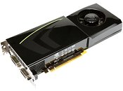
It has been noted on Newegg.com, a leading online retailer, that price-cuts have been injected across brands for the GeForce GTX 280. The card is now available for as low as US $314.99 for the MSI N280GTX-T2D1G OC (a factory overclocked card) with prices of reference-design cards staying below $360 for most of the available products. Leading vendors such as BFGTech, EVGA, and Zotac have placed their base models around the $320 range with factory overclocked models ranging around the $350 mark. The GeForce GTX 280 will be suceeded by the GeForce GTX 285 that is expected to launch on 15th January, which sports a refreshed G200b graphics processor built on the 55nm manufacturing process and running at higher clock speeds. NVIDIA has resorted to similar price-cuts for its GeForce GTX 260 graphics accelerator to serve two purposes: making the product attractive during the crucial Christmas shopping season, and to digest inventories for the 55nm GeForce GTX 260 launch.

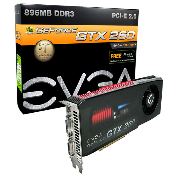
EVGA 55nm GeForce GTX 260 Ready for Launch
With NVIDIA being ready with variants of the G200 graphics processors based on the 55nm manufacturing process, a fleet of new graphics cards are in the line for launches. The range starts with a sub-$300 offering, the GeForce GTX 260 55nm. You now have three SKUs that share the name "GeForce GTX 260". The GeForce GTX 260 comes with the 216 SP configuration with 896 MB of GDDR3 memory. EVGA for one, is aiming to be one of the first NVIDIA partners to be out with the new GeForce GTX 260, with a standard and Superclocked models ready for launch, already listed in European and North American online stores.
The EVGA 896-P3-1255-AR comes with NVIDIA reference clock speeds of 576 MHz (core), 1242 MHz (shader) and 999 MHz (memory), while the Superclocked EVGA 896-P3-1257-AR model is factory-overclocked with 626 MHz (core), 1350 MHz (shader) and 1053 MHz (memory). EVGA is further planning a SSC variant that could come with a core clock speed of 666 MHz. For now, American retailer ZipZoomFly has listed the reference speed card for $289.99 and the Superclocked variant for just $4 more. Both cards are listed as "pre-order".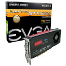

The EVGA 896-P3-1255-AR comes with NVIDIA reference clock speeds of 576 MHz (core), 1242 MHz (shader) and 999 MHz (memory), while the Superclocked EVGA 896-P3-1257-AR model is factory-overclocked with 626 MHz (core), 1350 MHz (shader) and 1053 MHz (memory). EVGA is further planning a SSC variant that could come with a core clock speed of 666 MHz. For now, American retailer ZipZoomFly has listed the reference speed card for $289.99 and the Superclocked variant for just $4 more. Both cards are listed as "pre-order".

NVIDIA to Launch GT300 in Q1 2009?
The tentative release time-frames for upcoming GPUs by NVIDIA and AMD have been seesawing between early 2009 and Q4 2009 for some time now. Industrial sources tell DigiTimes, that NVIDIA will be launching the GT300 graphics processor as early as in Q1 2009. What's even more surprising according to the report, is that the new GPU will be built on the 55nm manufacturing node of its foundry partners.
In related news, NVIDIA will be showcasing its range of products based on the 55nm G200b core at CES 2009, which starts on January 8. The notable products include a dual-GPU card, the GeForce GTX 295, and the single GPU flagship product, the GeForce GTX 285. NVIDIA refused to comment on the report.
In related news, NVIDIA will be showcasing its range of products based on the 55nm G200b core at CES 2009, which starts on January 8. The notable products include a dual-GPU card, the GeForce GTX 295, and the single GPU flagship product, the GeForce GTX 285. NVIDIA refused to comment on the report.

Power and Innovation to Drive High-End GPUs in 2009
The year 2008 so far, has been very eventful for the graphics card market. A reinvigorated GPU lineup by ATI, brought in some fierce competition to NVIDIA, which resulted in a tug-of-war with pricing graphics cards in the market, with either company refusing to lose on grounds of pricing. This event, coupled with the announcement of several game titles by game publishers, resulted in bumper-sales of graphics cards, giving the present state of the global economy little or no relevance.
The months to come hold the same amount of importance for both AMD and NVIDIA, where the next round of competition begins with successors to current high-end products being slated. NVIDIA is expected to continue with its monolithic high transistor-count GPU design methodology, while AMD could bring in a little change to the way it uses two efficient GPUs to build powerful products.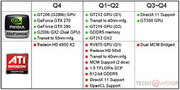
The months to come hold the same amount of importance for both AMD and NVIDIA, where the next round of competition begins with successors to current high-end products being slated. NVIDIA is expected to continue with its monolithic high transistor-count GPU design methodology, while AMD could bring in a little change to the way it uses two efficient GPUs to build powerful products.

40nm High-End NVIDIA GPUs Slated for 2009, GT206 for Q4
NVIDIA is expected to continue on its monolithic high-end GPU approach with a few notable GPUs that have been slated for Q4, 2008 and throughout 2009. The visual computing giant will be rolling out a 55nm derivative of the existing G200 graphics processor, codenamed GT206. The GPU is expected to be essentially the same, albeit newer silicon process allowing higher clock-speeds, that push up the performance envelope. The GT206 will be released in Q4, 2008., presumably to cash-in on the X-mas shopping season. It is found that GT206 seems to be having problems with its shader domain, which has pushed its launch for that late.
Following GT206, GT212 and GT216 would be NVIDIA's entries to the 40nm silicon fabrication process. Earlier reports suggested that foundry companies in Taiwan could be ready with the infrastructure to manufacture 40nm GPUs by June/July 2009. For the late second quarter 2009, either GT212, GT216, or simply a new card based the GT206, in a dual-GPU configuration could lead the pack. GT212 and GT216 could release in Q2, 2009. The GT212, GT216 GPUs support GDDR5 memory on a broad memory bus. Towards the end of the year however, NVIDIA will have made its DirectX 11 GPU, the GT300.
Following GT206, GT212 and GT216 would be NVIDIA's entries to the 40nm silicon fabrication process. Earlier reports suggested that foundry companies in Taiwan could be ready with the infrastructure to manufacture 40nm GPUs by June/July 2009. For the late second quarter 2009, either GT212, GT216, or simply a new card based the GT206, in a dual-GPU configuration could lead the pack. GT212 and GT216 could release in Q2, 2009. The GT212, GT216 GPUs support GDDR5 memory on a broad memory bus. Towards the end of the year however, NVIDIA will have made its DirectX 11 GPU, the GT300.
NVIDIA to Change GPU Nomenclature
Industry sources report, NVIDIA could be bringing about a massive nomenclature change, departing from its current GeForce 9000 series, to a newer naming system. And we're talking about the brand name here, not the GPU code name (such as G80, G92, G200, etc.) On October 15, the company is rumored to launch new graphics processors under the GT200 series. That's when it is noted that the company breaks away from its current nomenclature for GeForce 9xxx. One of the reasons known so far, is that the company wants to use its transition to the 55nm fab processors as a brand determining factor, easing confusion it has created when products made with the new processors share product names with the current 65nm GPUs.
On to the nomenclature itself, and "GTX 200" would be the series that accommodates extreme performance, enthusiast-grade products. This is already implemented. "GT 200" for high-performance GPUs, followed by "GS 200" for mainstream graphics products, and finally "G200" for entry-level products. Again, we're talking about the model numbers that make it to SKUs, product boxes, etc., not the GPU code-names. Regarding current GeForce 9000 series, they would be rebranded as G100, GT120, GT130, GT140 and GT150, bottom thru top. It is expected that the transition to this new naming system would be completed by Q1 thru Q2, 2009, as that's when NVIDIA is expected to release new enthusiast-grade GPUs based on the even newer 45nm silicon fabrication process.
On to the nomenclature itself, and "GTX 200" would be the series that accommodates extreme performance, enthusiast-grade products. This is already implemented. "GT 200" for high-performance GPUs, followed by "GS 200" for mainstream graphics products, and finally "G200" for entry-level products. Again, we're talking about the model numbers that make it to SKUs, product boxes, etc., not the GPU code-names. Regarding current GeForce 9000 series, they would be rebranded as G100, GT120, GT130, GT140 and GT150, bottom thru top. It is expected that the transition to this new naming system would be completed by Q1 thru Q2, 2009, as that's when NVIDIA is expected to release new enthusiast-grade GPUs based on the even newer 45nm silicon fabrication process.
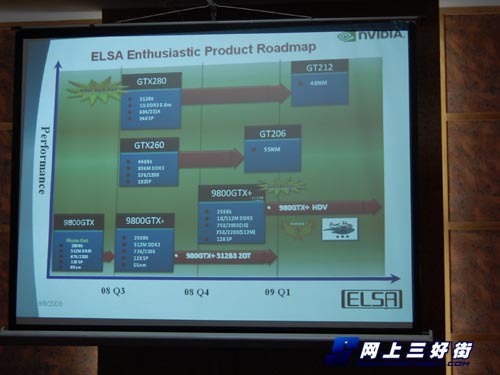
ELSA Slide Shows GTX 200 Series Successors
Slides published during a press meeting held at ELSA's headquarters in Shenzhen, China reveals what look like NVIDIA's future graphics processors (GPU). Although not quite playing on the global stage, ELSA is a popular channel vendor operating in China that concentrates on Asian markets. ELSA showcased several of its products. During a press event where its consumer graphics plans were discussed, ELSA published a slide that shows two future GPUs from NVIDIA, codenamed GT206 and GT212. These GPUs are positioned to succeed current flagship GPUs as in the G200. The slide shows a graph with launch time on the x-axis and performance projection on the y-axis. It can be inferred that GT206 is going to succeed the current GeForce GTX 260 and the GT212 succeeds GTX 280. Time scales show that GT206 comes out towards the very end of this year, and GT212 comes out sometime in Q1, 2009.
NVIDIA Plans to Nuke R700
NVIDIA Plans to Nuke R700?
Let's face it, the ATI RV770 and its derivatives have become a rage. Everybody loves this chip and wants a card based on this, be it the card that made NVIDIA slash their prices, the HD4850 or the HD4870 which rivals the GeForce GTX 260 at a decent price. In surveys conducted by several websites, be it TweakTown or Hexus.net, majority community members chose ATI as a brand over NVIDIA, rougly indicating that the HD4000 series has done an excellent repair job with ATI and its brand value.
Nothing (exciting) is going NVIDIA's way these days, their notebook graphics division has taken a beating over the recent faulty parts issue. The NVDA stock is a little volatile at the stock market these days, after the company announced it predicts weaker earnings this quarter financial year. Here's something to ponder: If NVIDIA predicts weaker earnings, how come talks are they have something to counter the R700, which AMD already made statements about, saying it will "overwhelm the GeForce GTX 280"?
NVIDIA in a Rush for 55nm Parts, has Partners 'Red-Eyed'
With the cost of manufacture for a standard G200 die reaching up to US $110, thanks to yields as low as 40 per cent, NVIDIA seems to be in a rush for a 55nm revamp of its current GPUs. While nothing revolutionary is on the cards, and with 55nm G92b already in the making, NVIDIA plans to revamp its G200 graphics processors to the 55nm fab process, increasing yields up to 50 per cent. At 55nm, the G200 die will be effectively reduced to 470 sq. mm, implies 120 dice on a 300mm wafer.
The pace at which things are moving is having the partners red-eyed. NVIDIA's new Unilateral Minimum Advertised Price Policy (UMAP) has limited partners' playing field and minimizes competition between them. When NVIDIA at the same time decides to launch new cards based on existing cores, at lower prices, partners get upset over diminishing earnings. Add to that AMD's new RV770 chip is looking very tempting to some of these partners.
The pace at which things are moving is having the partners red-eyed. NVIDIA's new Unilateral Minimum Advertised Price Policy (UMAP) has limited partners' playing field and minimizes competition between them. When NVIDIA at the same time decides to launch new cards based on existing cores, at lower prices, partners get upset over diminishing earnings. Add to that AMD's new RV770 chip is looking very tempting to some of these partners.
Apr 18th, 2025 15:46 EDT
change timezone
Latest GPU Drivers
New Forum Posts
- Place your bets, what node will rtx 6000/RDNA 5(UDNA 1?) use (8)
- Can Intel recover in DYI market anytime soon? (10)
- TPU's Nostalgic Hardware Club (20257)
- GPU Pricing and Performance (15)
- What are you playing? (23396)
- Spoofer Modified SMBIOS/BIOS – Need Help Restoring Original Motherboard Info (TUF GAMING B550-PLUS WiFi II) (2)
- Tried installing 576.02 - installer window disappears (20)
- RX 9000 series GPU Owners Club (392)
- GPU Database (300)
- Drives fail to work with Rufus Windows TO GO (2)
Popular Reviews
- ASUS GeForce RTX 5060 Ti TUF OC 16 GB Review
- NVIDIA GeForce RTX 5060 Ti PCI-Express x8 Scaling
- Palit GeForce RTX 5060 Ti Infinity 3 16 GB Review
- G.SKILL Trident Z5 NEO RGB DDR5-6000 32 GB CL26 Review - AMD EXPO
- ASUS GeForce RTX 5060 Ti Prime OC 16 GB Review
- Teevolution Terra Pro Review
- MSI GeForce RTX 5060 Ti Gaming OC 16 GB Review
- Zotac GeForce RTX 5060 Ti AMP 16 GB Review
- MSI GeForce RTX 5060 Ti Gaming Trio OC 16 GB Review
- ASUS GeForce RTX 5080 TUF OC Review
Controversial News Posts
- NVIDIA GeForce RTX 5060 Ti 16 GB SKU Likely Launching at $499, According to Supply Chain Leak (182)
- NVIDIA Sends MSRP Numbers to Partners: GeForce RTX 5060 Ti 8 GB at $379, RTX 5060 Ti 16 GB at $429 (127)
- Nintendo Confirms That Switch 2 Joy-Cons Will Not Utilize Hall Effect Stick Technology (105)
- Over 200,000 Sold Radeon RX 9070 and RX 9070 XT GPUs? AMD Says No Number was Given (100)
- NVIDIA Launches GeForce RTX 5060 Series, Beginning with RTX 5060 Ti This Week (100)
- Nintendo Switch 2 Launches June 5 at $449.99 with New Hardware and Games (99)
- Sony Increases the PS5 Pricing in EMEA and ANZ by Around 25 Percent (85)
- NVIDIA PhysX and Flow Made Fully Open-Source (77)