News Posts matching #GDDR7

Return to Keyword Browsing

Passive Buyer Strategies Drive DRAM Contract Prices Down Across the Board in 1Q25

TrendForce's latest investigations reveal that the DRAM market is expected to face downward pricing pressure in 1Q25 as seasonal weakness aligns with sluggish consumer demand for products like smartphones. Additionally, early stockpiling by notebook manufacturers—over potential import tariffs under the Trump administration—has further exacerbated the pricing decline.

Conventional DRAM prices are projected to drop by 8% to 13%. However, if HBM products are included, the anticipated price decline will range from 0% to 5%.

NVIDIA GeForce RTX 5090 Features 16+6+7 Phase Power Delivery on 14-Layer PCB

Fresh details have surfaced about NVIDIA's upcoming flagship "Blackwell" graphics card, the GeForce RTX 5090, suggesting power delivery and board design changes compared to its predecessors. According to Benchlife, the new Blackwell-based GPU will feature a new 16+6+7 power stage design, departing from the RTX 4090's 20+3 phase configuration. The report confirms earlier speculation about the card's power requirements, indicating a TGP of 600 watts. This specification refers to the complete power allocation for the graphics subsystem, though the actual TDP of the GB202 chip might be lower. The RTX 5090 will ship with 32 GB of next-generation GDDR7 memory and utilize a 14-layer PCB, possibly due to the increased complexity of GDDR7 memory modules and power delivery. Usually, GPUs max out at 12 layers for high-end overclocking designs.

The upcoming GPU will fully embrace modern connectivity standards, featuring PCI Express 5.0 x16 interface compatibility and implementing a 12V-2×6 power connector design. We spotted an early PNY RTX 5090 model with 40 capacitors but an unclear power delivery setup. With additional power phases and more PCB layers, NVIDIA is pushing the power delivery and signal integrity boundaries for its next-generation flagship. While these specifications paint a picture of a powerful gaming and professional graphics solution, questions remain about the broader RTX 50 series lineup. The implementation of the 12V-2×6 connector across different models, particularly those below 200 W, remains unclear, so we have to wait for the CES-rumored launch.

NVIDIA GeForce RTX 5090 Powered by "GB202" Silicon, 512-bit GDDR7, ASIC Pictured

Here is the first picture of what is very likely the GeForce RTX 5090 "Blackwell," the successor to the RTX 4090 "Ada." The picture, its massive GPU, and layout appear to confirm the weekend's bare PCB leak. The RTX 5090 is powered by the "GB202" silicon, the largest gaming GPU based on the "Blackwell" graphics architecture. The silicon in the picture has the ASIC code "GB202-300-A1." From this ASIC code, we can deduce that the RTX 5090 may not max out the silicon (i.e. enable all SM present on it), as maxed-out NVIDIA ASICs tend to have the variant designation "450."

The "GB202" ASIC is surrounded by sixteen GDDR7 memory chips, which reportedly make the 32 GB memory size of the RTX 5090. The chip count, coupled with the large GPU package size (high pin-count), confirm that the "GB202" features a 512-bit wide memory bus. Assuming a memory speed of 28 Gbps, this memory bus should yield a stellar memory bandwidth of 1,792 GB/s. The GPU and memory are surrounded by the card's 24-phase VRM solution. This draws power from a single 16-pin 12V-2x6 power connector. NVIDIA will likely max out the 600 W continuous power-delivery capability of the connector, and give the card a TGP of around 500-550 W, if not more.

NVIDIA GeForce RTX 5070 and RTX 5070 Ti Final Specifications Seemingly Confirmed

Thanks to kopite7kimi, we are able to finalize the leaked specifications of NVIDIA's upcoming GeForce RTX 5070 and RTX 5070 Ti graphics cards.
Starting off with RTX 5070 Ti, it will feature 8,960 CUDA cores and come equipped with 16 GB GDDR7 memory on a 256-bit memory bus, offering 896 GB/s bandwidth. The card is reportedly designed with a total board power (TBP) of 300 W. The Ti variant appears to use the PG147-SKU60 board design with a GB203-300-A1 GPU. The standard RTX 5070 is positioned as a more power-efficient option, with specifications pointing to 6,144 CUDA cores and 12 GB of GDDR7 memory on a 192-bit bus, with 627 GB/s memory bandwidth. This model is expected to operate at a slightly lower 250 W TBP.

Interestingly, the non-Ti RTX 5070 card will be available in two board variants, PG146 and PG147, both utilizing the GB205-300-A1 GPU. While we don't know what the pricing structure looks like, we see that NVIDIA has chosen to make more considerable differentiating factors between its SKUs. The Ti variant not only gets an extra four GB of GDDR7 memory, but it also gets a whopping 45% increase in CUDA core count, going from 6,144 to 8,960 cores. While we wait for the CES to see the initial wave of GeForce RTX 50 series cards, the GeForce RTX 5070 and RTX 5070 Ti are expected to arrive later, possibly after RTX 5080 and RTX 5090 GPUs.

NVIDIA GeForce RTX 5090 PCB Pictured, Massive GPU Die and 16-Chip Memory Configuration

NVIDIA's GeForce RTX 5090 graphics card printed circuit board has allegedly been shown in the flesh, showing the memory layout and some interesting engineering choices. The custom PCB variant (non-Founders Edition) houses more than 40 capacitors, which is perhaps not standard on the FE reference board, and 16 GDDR7 memory modules. The leaked PCB, which extends beyond standard dimensions and traditional display connector configurations, is reportedly based on NVIDIA's PG145 reference design. The memory modules are distributed systematically: five on the left, two below, five on the right, and four above the GPU die. The interface is PCIe 5.0 x16.

As NVIDIA has reportedly designated 32 GB GDDR7 memory capacity for these cards, this roughly translates into 16 x 2 GB GDDR7 memory modules. At the heart of the card lies what sources claim to be the GB202 GPU, measuring 24×31 mm within a 63×56 mm package. Power delivery uses a 16-pin 12V-6x2 power connector, as expected. The entire PCB features only a single power connector, so the 16-pin 12V-2x6, but with an updated PCIe 6.0 CEM specification, is the logical choice.

NVIDIA GeForce RTX 5080 to Stand Out with 30 Gbps GDDR7 Memory, Other SKUs Remain on 28 Gbps

NVIDIA is preparing to unveil its "Blackwell" GeForce RTX 5080 graphics card, featuring cutting-edge GDDR7 memory technology. However, RTX 5080 is expected to be equipped with 16 GB of GDDR7 memory running at an impressive 30 Gbps. Combined with a 256-bit memory bus, this configuration will deliver approximately 960 GB/s bandwidth—a 34% improvement over its predecessor, the RTX 4080, which operates at 716.8 GB/s. While the RTX 5080 will stand as the sole card in the lineup featuring 30 Gbps memory modules, while other models in the RTX 50 series will incorporate slightly slower 28 Gbps variants. This strategic differentiation is possibly due to the massive CUDA cores gap between the rumored RTX 5080 and RTX 5090.

The flagship RTX 5090 is set to push boundaries even further, implementing a wider 512-bit memory bus that could potentially achieve bandwidth exceeding 1.7 TB/s. NVIDIA appears to be reserving larger memory configurations of 16 GB+ exclusively for this top-tier model, at least until higher-capacity GDDR7 modules become available in the market. Despite these impressive specifications, the RTX 5080's bandwidth still falls approximately 5% short of the current RTX 4090, which benefits from a physically wider bus configuration. This performance gap between the 5080 and the anticipated 5090 suggests NVIDIA is maintaining a clear hierarchy within its product stack, and we have to wait for the final launch to conclude what, how, and why of the Blackwell gaming GPUs.

NVIDIA GeForce RTX 5070 Ti Leak Tips More VRAM, Cores, and Power Draw

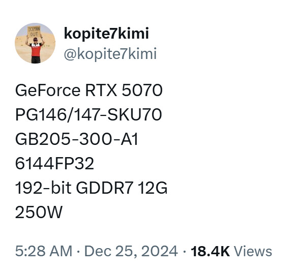
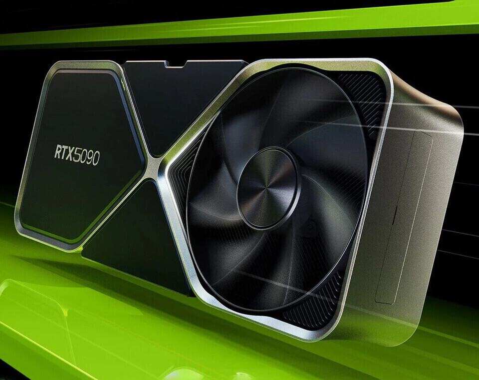
It's an open secret by now that NVIDIA's GeForce RTX 5000 series GPUs are on the way, with an early 2025 launch on the cards. Now, preliminary details about the 
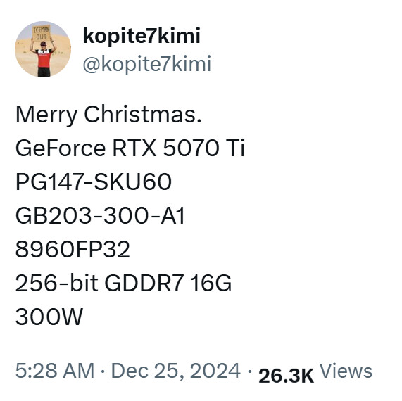
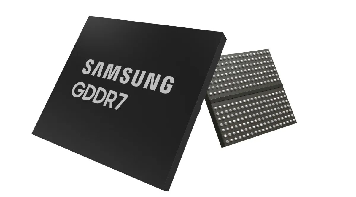
RTX 5070 Ti have leaked, revealing an increase in both VRAM and TDP and suggesting that the new upper mid-range GPU will finally address the increased VRAM demand from modern games. According to the leak from Wccftech, the RTX 5070 Ti will have 16 GB of GDDR7 VRAM, up from 12 GB on the RTX 4070 Ti, as we 
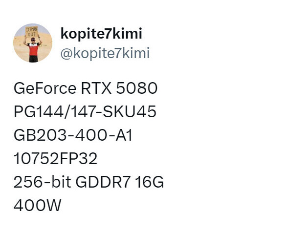
previously speculated. Also confirming previous leaks, the new sources confirm that the 5070 Ti will use the cut-down GB203 chip, although the new leak points to a significantly higher TBP of 350 W. The new memory configuration will supposedly run on a 256-bit memory bus and run at 28 Gbps for a total memory bandwidth of 896 GB/s, which is a significant boost over the RTX 4070 Ti.

Supposedly, the RTX 5070 Ti will also see a bump in total CUDA cores, from 7680 in the RTX 4070 Ti to 8960 in the RTX 5070 Ti. The new RTX 5070 Ti will also switch to the 12V-2x6 power connector, compared to the 16-pin connector from the 4070 Ti. NVIDIA is expected to announce the RTX 5000 series graphics cards at CES 2025 in early January, but the RTX 5070 Ti will supposedly be the third card in the 5000-series launch cycle. That said, leaks suggest that the 5070 Ti will still launch in Q1 2025, meaning we may see an indication of specs at CES 2025, although pricing is still unclear.

Update Dec 16th: Kopite7kimi, ubiquitous hardware leaker, has since responded to the RTX 5070 Ti leaks, stating that 350 W may be on the higher end for the RTX 5070 Ti: "...the latest data shows 285W. However, 350W is also one of the configs." This could mean that a TBP of 350 W is possible, although maybe only on certain graphics card models, if competition is strong, or in certain boost scenarios.

Possible NVIDIA GeForce RTX 5080 Laptop GPU Pictured

Could this be the first picture of an NVIDIA GeForce RTX 5080 Laptop GPU? This picture, coupled with a specs sheet by notebook OEM Clevo, seems to suggest so, thanks to a new video by Moore's Law is Dead. The chip is noticeably more rectangular than the Ada "AD104," and is labelled N22W-ES-A1. It is an engineering sample. Cross-referencing "N22W" with the Clevo specs-sheet for a next-generation laptop mainboard, points to the possibility that the chip is indeed based on a next-gen silicon by NVIDIA. The board design has to undergo a significant change, due to the major change in the pin-map of the fiberglass substrate brought about by the switch to the new GDDR7 memory type.

The GeForce "Blackwell" generation comes in several GPU silicon sizes, and the RTX 5080 Laptop GPU is expected to be based on the "GB203" chip, which is expected to power the desktop RTX 5080 and possibly some SKUs in even the RTX 5070 series, such as the "RTX 5070 Ti." It is rumored to feature as many as 8,192 CUDA cores, and a 256-bit wide GDDR7 memory interface. NVIDIA is expected to unveil the GeForce "Blackwell" generation at CES 2025.

NVIDIA Tunes GeForce RTX 5080 GDDR7 Memory to 32 Gbps, RTX 5070 Launches at CES

NVIDIA is gearing up for an exciting showcase at CES 2025, where its CEO, Jensen Huang, will take the stage and talk about, hopefully, future "Blackwell" products. According to Wccftech's sources, the anticipated GeForce RTX 5090, RTX 5080, and RTX 5070 graphics cards should arrive at CES 2025 in January. The flagship RTX 5090 is rumored to come equipped with 32 GB of GDDR7 memory running at 28 Gbps. Meanwhile, the RTX 5080 looks very interesting with reports of its impressive 16 GB of GDDR7 memory running at 32 Gbps. This advancement comes after we previously believed that the RTX 5080 model is going to feature 28 Gbps GDDR7 memory. However, the newest rumors suggest that we are in for a surprise, as the massive gap between RTX 5090 and RTX 5080 compute cores will be filled... with a faster memory.

The more budget-friendly RTX 5070 is also set for a CES debut, featuring 12 GB of memory. This card aims to deliver solid performance for gamers who want high-quality graphics without breaking the bank, targeting the mid-range segment. We are very curious about pricing of these models and how they would fit in the current market. As anticipation builds for CES 2025, we are eager to see how these innovations will impact gaming experiences and creative workflows in the coming year. Stay tuned for more updates as the event approaches!

NVIDIA GeForce RTX 5090 and RTX 5080 Specifications Surface, Showing Larger SKU Segmentation

Thanks to the renowned NVIDIA hardware leaker kopite7Kimi on X, we are getting information about the final versions of NVIDIA's first upcoming wave of GeForce RTX 50 series "Blackwell" graphics cards. The two leaked GPUs are the GeForce RTX 5090 and RTX 5080, which now feature a more significant gap between xx80 and xx90 SKUs. For starters, we have the highest-end GeForce RTX 5090. NVIDIA has decided to use the GB202-300-A1 die and enabled 21,760 FP32 CUDA cores on this top-end model. Accompanying the massive 170 SM GPU configuration, the RTX 5090 has 32 GB of GDDR7 memory on a 512-bit bus, with each GDDR7 die running at 28 Gbps. This translates to 1,568 GB/s memory bandwidth. All of this is confined to a 600 W TGP.

When it comes to the GeForce RTX 5080, NVIDIA has decided to further separate its xx80 and xx90 SKUs. The RTX 5080 has 10,752 FP32 CUDA cores paired with 16 GB of GDDR7 memory on a 256-bit bus. With GDDR7 running at 28 Gbps, the memory bandwidth is also halved at 784 GB/s. This SKU uses a GB203-400-A1 die, which is designed to run within a 400 W TGP power envelope. For reference, the RTX 4090 has 68% more CUDA cores than the RTX 4080. The rumored RTX 5090 has around 102% more CUDA cores than the rumored RTX 5080, which means that NVIDIA is separating its top SKUs even more. We are curious to see at what price point NVIDIA places its upcoming GPUs so that we can compare generational updates and the difference between xx80 and xx90 models and their widened gaps.

NVIDIA GeForce RTX 5090 and RTX 5080 Reach Final Stages This Month, Chinese "D" Variant Arrives for Both SKUs

NVIDIA is on the brink of finalizing its next-generation "Blackwell" graphics cards, the GeForce RTX 5090 and RTX 5080. Sources close to BenchLife indicate that NVIDIA is targeting September for the official design specification finalization of both models. This timeline hints at a possible unveiling at CES 2025, with a market release shortly after. The RTX 5090 is rumored to boast a staggering 550 W TGP, a significant 22% increase from its predecessor, the RTX 4090. Meanwhile, the RTX 5080 is expected to draw 350 W, a more modest 9.3% bump from the current RTX 4080. Interestingly, NVIDIA appears to be developing "D" variants for both cards, which are likely tailored for the Chinese market to comply with export regulations.

Regarding raw power, the RTX 5090 is speculated to feature 24,576 CUDA cores paired with 512-bit GDDR7 memory. The RTX 5080, while less mighty, is still expected to pack a punch with 10,752 CUDA cores and 256-bit GDDR7 memory. As NVIDIA prepares to launch these powerhouses, rumors suggest the RTX 4090D may be discontinued by December 2024, paving the way for its successor. We are curious to see how the power consumption is handled and if these cards are packed efficiently within the higher power envelope. Some rumors indicate that the RTX 5090 could reach 600 watts at its peak, while RTX 5080 reaches 400 watts. However, that is just a rumor for now. As always, until NVIDIA makes an official announcement, these details should be taken with a grain of salt.

NVIDIA's RTX 5060 "Blackwell" Laptop GPU Comes with 8 GB of GDDR7 Memory Running at 28 Gbps, 25 W Lower TGP

In a recent event hosted by Chinese laptop manufacturer Hasee, company's chairman Wu Haijun unveiled exciting details about NVIDIA's upcoming GeForce RTX 5060 "Blackwell" laptop GPU. Attending the event was industry insider Golden Pig Upgrade, who managed to catch some details of the card set to launch next year. The RTX 5060 is expected to be the first in the market to feature GDDR7 memory, a move that aligns with earlier leaks suggesting NVIDIA's entire Blackwell lineup would adopt this new standard. This upgrade is anticipated to deliver substantial boosts in bandwidth and possibly increased VRAM capacities in other SKUs. Perhaps most intriguing is the reported performance of the RTX 5060. Wu said this laptop SKU could offer performance comparable to the current RTX 4070 laptop GPU. It's said to exceed the RTX 4070 in ray tracing scenarios and match or come close to its rasterization performance.

This leap in capabilities is made even more impressive by the chip's reduced power consumption, with a maximum TGP of 115 W compared to the RTX 4060's 140 W. The reported power efficiency gains are not exclusive to RTX 5060. Wu suggests that the entire Blackwell lineup will see significant reductions in power draw, potentially lowering overall system power consumption by 40 to 50 watts in many Blackwell models. While specific technical details remain limited, it's believed the RTX 5060 will utilize the GB206 GPU die paired with 8 GB of GDDR7 memory, likely running at 28 Gbps in its initial iteration.

SK hynix Launches Its New GDDR7 Graphics Memory

SK hynix Inc. announced today that it introduced the industry's best-performing GDDR7, a next-generation graphics memory product. The development of GDDR7 in March comes amid growing interest by global customers in the AI space in the DRAM product that meets both specialized performance for graphics processing and fast speed. The company said that it will start volume production in the third quarter.

The new product comes with the operating speed of 32 Gbps, a 60% improvement from the previous generation and the speed can grow up to 40 Gbps depending on the circumstances. When adopted for the high-end graphics cards, the product can also process data of more than 1.5 TB per second, equivalent to 300 Full-HD movies (5 GB each), in a second.

DRAM Prices Expected to Increase by 8-13% in Q3

TrendForce reports that a recovery in demand for general servers—coupled with an increased production share of HBM by DRAM suppliers—has led suppliers to maintain their stance on hiking prices. As a result, the ASP of DRAM in the third quarter is expected to continue rising, with an anticipated increase of 8-13%. The price of conventional DRAM is expected to rise by 5-10%, showing a slight contraction compared to the increase in the second quarter.

TrendForce notes that buyers were more conservative about restocking in the second, and inventory levels on both the supplier and buyer sides did not show significant changes. Looking ahead to the third quarter, there is still room for inventory replenishment for smartphones and CSPs, and the peak season for production is soon to commence. Consequently, it is expected that smartphones and servers will drive an increase in memory shipments in the third quarter.

Samsung, SK Hynix, and Micron Compete for GDDR7 Dominance

Competition among Samsung, SK Hynix, and Micron is intensifying, with a focus on enhancing processing speed and efficiency in graphics DRAM (GDDR) for AI accelerators and cryptocurrency mining. Compared with High Bandwidth Memory (HBM), the GDDR7 has a faster data processing speed and a relatively low price. Since Nvidia is expected to use next-generation GDDR7 with its GeForce RTX50 Blackwell GPUs, competition will likely be as strong as the demand. We can see that by looking, for example, at the pace of new GDDR7 releases from the past two years.

In July 2022, Samsung Electronics developed the industry's first 32 Gbps GDDR7 DRAM, capable of processing up to 1.5 TB of data per second, a 1.4 times speed increase and 20% better energy efficiency compared to GDDR6. In February 2023, Samsung demonstrated its first GDDR7 DRAM with a pin rate of 37 Gbps. On June 4, Micron launched its new GDDR7 at Computex 2024, with speeds up to 32 Gbps, a 60% increase in bandwidth, and a 50% improvement in energy efficiency over the previous generation. Shortly after, SK Hynix introduced a 40 Gbps GDDR7, showcased again at Computex 2024, doubling the previous generation's bandwidth to 128 GB per second and improving energy efficiency by 40%.

SK Hynix Targets Q1 2025 for GDDR7 Memory Mass Production

The race is on for memory manufacturers to bring the next generation GDDR7 graphics memory into mass production. While rivals Samsung and Micron are aiming to have GDDR7 chips available in Q4 of 2024, South Korean semiconductor giant SK Hynix revealed at Computex 2024 that it won't kick off mass production until the first quarter of 2025. GDDR7 is the upcoming JEDEC standard for high-performance graphics memory, succeeding the current GDDR6 and GDDR6X specifications. The new tech promises significantly increased bandwidth and capacities to feed the appetites of next-wave GPUs and AI accelerators. At its Computex booth, SK Hynix showed off engineering samples of its forthcoming GDDR7 chips, with plans for both 16 Gb and 24 Gb densities.

The company is targeting blazing-fast 40 Gbps data transfer rates with its GDDR7 offerings, outpacing the 32 Gbps rates its competitors are starting with on 16 Gb parts. If realized, higher speeds could give SK Hynix an edge, at least initially. While trailing a quarter or two behind Micron and Samsung isn't ideal, SK Hynix claims having working samples now validates its design and allows partners to begin testing and qualification. Mass production timing for standardized memories also doesn't necessarily indicate a company is "late" - it simply means another vendor secured an earlier production window with a specific customer. The GDDR7 transition is critical for SK Hynix and others, given the insatiable demand for high-bandwidth memory to power AI, graphics, and other data-intensive workloads. Hitting its stated Q1 2025 mass production target could ensure SK Hynix doesn't fall too far behind in the high-stakes GDDR7 race, with faster and higher-density chips to potentially follow shortly after volume ramp.

Possible Specs of NVIDIA GeForce "Blackwell" GPU Lineup Leaked

Possible specifications of the various NVIDIA GeForce "Blackwell" gaming GPUs were leaked to the web by Kopite7kimi, a reliable source with NVIDIA leaks. These are specs of the maxed out silicon, NVIDIA will carve out several GeForce RTX 50-series SKUs based on these chips, which could end up with lower shader counts than those shown here. We've known from older reports that there will be five chips in all, the GB202 being the largest, followed by the GB203, the GB205, the GB206, and the GB207. There is a notable absence of a successor to the AD104, GA104, and TU104, because NVIDIA is trying a slightly different way to approach the performance segment with this generation.

The GB202 is the halo segment chip that will drive the possible RTX 5090 (RTX 4090 successor). This chip is endowed with 192 streaming multiprocessors (SM), or 96 texture processing clusters (TPCs). These 96 TPCs are spread across 12 graphics processing clusters (GPCs), which each have 8 of them. Assuming that "Blackwell" has the same 256 CUDA cores per TPC that the past several generations of NVIDIA gaming GPUs have had, we end up with a total CUDA core count of 24,576. Another interesting aspect about this mega-chip is memory. The GPU implements the next-generation GDDR7 memory, and uses a mammoth 512-bit memory bus. Assuming the 28 Gbps memory speed that was being rumored for NVIDIA's "Blackwell" generation, this chip has 1,792 GB/s of memory bandwidth on tap!

First NVIDIA RTX 5090 Performance View? Micron Knows Better

Micron is getting ready to set sail with the new GDDR7 memory, and being NVIDIA's long-term partner, both are gaining big with the GeForce RTX 4000 Series. A few days ago, Micron announced its imminent launch of GDDR7 memory, remember that in March JEDEC published the GDDR7 memory standard. The interesting part is that an even more important piece of information was provided in one of Micron's slide-deck, the one that shows GDDR7 gaming performance. Officially Micron says that GDDR7 can be 3.1x faster than GDDR6 and 1.5x faster than GDDR6X. However, the slide in question provides some normalized FPS performance for ray tracing, and rasterization under game testing conditions. Until now, everything is clear, what comes next is our speculation and assumptions, based on previous knowledge so please, take it with a grain of salt. Will it be a hard guess, looking over those graphs, to tell that NVIDIA's RTX 5090 offers up to a 42% improvement over the RTX 4090 in rasterization, and up to 48% in ray tracing?

NVIDIA is getting closer to releasing its next-gen GPU with the RTX 5090 graphics card. Micron is in a strong partnership with NVIDIA and it's expected that its next gen graphics cards will use Micron GDDR7 memory. Now, we know that, at least for Ray Tracing, one real-world benchmark is Cyberpunk 2077, and it could be also the case here, from the graphs it looks very much like Ray Tracing was tested with Path Tracing. For Rasterization performance another hard guess is that perhaps it's either Starfield or Assassin's Creed Mirage. Presumably, tests were made using also AMD RX 7900XTX, and NVIDIA RTX 4090 to get GDDR6 reference. Time will tell if we made the right prediction.

Micron Samples Next-Gen GDDR7 Graphics Memory for Gaming and AI, Over 1.5 TB/s of System Bandwidth

Micron Technology, Inc., today announced the sampling of its next-generation GDDR7 graphics memory with the industry's highest bit density. Leveraging Micron's 1β (1-beta) DRAM technology and innovative architecture, Micron GDDR7 delivers 32 Gb/s high-performance memory in a power-optimized design. With over 1.5 TB/s of system bandwidth, which is up to 60% higher bandwidth than GDDR6, and four independent channels to optimize workloads, Micron GDDR7 memory enables faster response times, smoother gameplay and reduced processing times.

GDDR7 also provides a greater than 50% power-efficiency improvement compared to GDDR6 to better thermals and lengthen battery life, while the new sleep mode reduces standby power by up to 70%. Advanced reliability, availability and serviceability (RAS) features on Micron GDDR7 enhance device dependability and data integrity without compromising performance, broadening the spectrum of applications for Micron GDDR7 to AI, gaming and high-performance computing workloads.

AMD's RDNA 4 GPUs Could Stick with 18 Gbps GDDR6 Memory

Today, we have the latest round of leaks that suggest that AMD's upcoming RDNA 4 graphics cards, codenamed the "RX 8000-series," might continue to rely on GDDR6 memory modules. According to Kepler on X, the next-generation GPUs from AMD are expected to feature 18 Gbps GDDR6 memory, marking the fourth consecutive RDNA architecture to employ this memory standard. While GDDR6 may not offer the same bandwidth capabilities as the newer GDDR7 standard, this decision does not necessarily imply that RDNA 4 GPUs will be slow performers. AMD's choice to stick with GDDR6 is likely driven by factors such as meeting specific memory bandwidth requirements and cost optimization for PCB designs. However, if the rumor of 18 Gbps GDDR6 memory proves accurate, it would represent a slight step back from the 18-20 Gbps GDDR6 memory used in AMD's current RDNA 3 offerings, such as the RX 7900 XT and RX 7900 XTX GPUs.

AMD's first generation RDNA used GDDR6 with 12-14 Gbps speeds, RDNA 2 came with GDDR6 at 14-18 Gbps, and the current RDNA 3 used 18-20 Gbps GDDR6. Without an increment in memory generation, speeds should stay the same at 18 Gbps. However, it is crucial to remember that leaks should be treated with skepticism, as AMD's final memory choices for RDNA 4 could change before the official launch. The decision to use GDDR6 versus GDDR7 could have significant implications in the upcoming battle between AMD, NVIDIA, and Intel's next-generation GPU architectures. If AMD indeed opts for GDDR6 while NVIDIA pivots to GDDR7 for its "Blackwell" GPUs, it could create a disparity in memory bandwidth performance between the competing products. All three major GPU manufacturers—AMD, NVIDIA, and Intel with its "Battlemage" architecture—are expected to unveil their next-generation offerings in the fall of this year. As we approach these highly anticipated releases, more concrete details on specifications and performance capabilities will emerge, providing a clearer picture of the competitive landscape.

Introspect Technology Ships World's First GDDR7 Memory Test System

Introspect Technology, a JEDEC member and a leading manufacturer of test and measurement instruments, announced today that it has shipped the M5512 GDDR7 Memory Test System, the world's first commercial solution for testing JEDEC's newly minted JESD239 Graphics Double Data Rate (GDDR7) SGRAM specification. This category-creating solution enables graphics memory engineers, GPU design engineers, product engineers in both memory and GPU spaces, and system integrators to rapidly bring up new GDDR7 memory devices, debug protocol errors, characterize signal integrity, and perform detailed memory read/write functional stress testing without requiring any other tool.

The GDDR7 specification is the latest industry standard that is aimed at the creation of high-bandwidth and high-capacity memory implementations for graphics processing, artificial intelligence (AI), and AI-intensive networking. Featuring pulse-amplitude modulation (PAM) and an improved signal to noise ratio compared to other PAM4 standards used in networking, the GDDR7 PAM3 modulation technology achieves greater power-efficiency while significantly increasing data transmission bandwidth over constrained electrical channels.

Product Pages of Samsung 28 Gbps and 32 Gbps GDDR7 Chips Go Live

Samsung is ready with a GDDR7 memory chip rated at an oddly-specific 28 Gbps. This speed aligns with the reported default memory speeds of next-generation NVIDIA GeForce RTX "Blackwell" GPUs. The Samsung GDDR7 memory chip bearing model number K4VAF325ZC-SC28, pictured below, ticks at 3500 MHz, yielding 28 Gbps (GDDR7-effective) memory speeds, and comes with a density of 16 Gbit (2 GB). This isn't Samsung's only GDDR7 chip at launch, the company also has a 32 Gbps high performance part that it built in hopes that certain high-end SKUs or professional graphics cards may implement it. The 32 Gbps GDDR7 chip, bearing the chip model number K4VAF325ZC-SC32, offers the same 16 Gbit density, but at a higher 4000 MHz clock. The Samsung website part-identification pages for both chips say that the parts are sampling to customers, which is usually just before it enters mass-production, and is marked "shipping."

SK hynix Presents the Future of AI Memory Solutions at NVIDIA GTC 2024

SK hynix is displaying its latest AI memory technologies at NVIDIA's GPU Technology Conference (GTC) 2024 held in San Jose from March 18-21. The annual AI developer conference is proceeding as an in-person event for the first time since the start of the pandemic, welcoming industry officials, tech decision makers, and business leaders. At the event, SK hynix is showcasing new memory solutions for AI and data centers alongside its established products.

Showcasing the Industry's Highest Standard of AI Memory
The AI revolution has continued to pick up pace as AI technologies spread their reach into various industries. In response, SK hynix is developing AI memory solutions capable of handling the vast amounts of data and processing power required by AI. At GTC 2024, the company is displaying some of these products, including its 12-layer HBM3E and Compute Express Link (CXL)1, under the slogan "Memory, The Power of AI". HBM3E, the fifth generation of HBM2, is the highest-specification DRAM for AI applications on the market. It offers the industry's highest capacity of 36 gigabytes (GB), a processing speed of 1.18 terabytes (TB) per second, and exceptional heat dissipation, making it particularly suitable for AI systems. On March 19, SK hynix announced it had become the first in the industry to mass-produce HBM3E.

NVIDIA to Implement GDDR7 Memory on Top-3 "Blackwell" GPUs

NVIDIA is confirmed to implement the GDDR7 memory standard with the top three GPU ASICs powering the next-generation "Blackwell" GeForce RTX 50-series, Tweaktown reports, citing XpeaGPU. By this, we mean the top three physical silicon types from which NVIDIA will carve out the majority of its SKUs. This would include the GB202, the GB203, and GB205; which will power successors to everything from the current RTX 4070 to the RTX 4090. NVIDIA is expected to build these chips on the TSMC 4N foundry node.

There will be certain GPU ASIC types in the "Blackwell" generation that will stick to older memory standards such as GDDR6 or even the GDDR6X. These would be successors to the current AD106 and AD107 ASICs, powering SKUs such as the RTX 4060 Ti, and below. NVIDIA co-developed the GDDR6X standard with Micron Technology, which is the chip's exclusive supplier to NVIDIA. GDDR6X scales up to 23 Gbps and 16 Gbit, which means NVIDIA can avail plenty of performance for the lower-end of its product stack using GDDR6X; especially considering that its GDDR7 implementation will only run at 28 Gbps, despite chips being available in the market for 32 Gbps, or even 36 Gbps. Even if NVIDIA chooses the regular GDDR6 standard for its entry-mainstream chips, the tech scales up to 20 Gbps.

SK hynix Unveils Highest-Performing SSD for AI PCs at NVIDIA GTC 2024

SK hynix unveiled a new consumer product based on its latest solid-state drive (SSD), PCB01, which boasts industry-leading performance levels at GPU Technology Conference (GTC) 2024. Hosted by NVIDIA in San Jose, California from March 18-21, GTC is one of the world's leading conferences for AI developers. Applied to on-device AI PCs, PCB01 is a PCIe fifth-generation SSD which recently had its performance and reliability verified by a major global customer. After completing product development in the first half of 2024, SK hynix plans to launch two versions of PCB01 by the end of the year which target both major technology companies and general consumers.

Optimized for AI PCs, Capable of Loading LLMs Within One Second
Offering the industry's highest sequential read speed of 14 gigabytes per second (GB/s) and a sequential write speed of 12 GB/s, PCB01 doubles the speed specifications of its previous generation. This enables the loading of LLMs required for AI learning and inference in less than one second. To make on-device AIs operational, PC manufacturers create a structure that stores an LLM in the PC's internal storage and quickly transfers the data to DRAMs for AI tasks. In this process, the PCB01 inside the PC efficiently supports the loading of LLMs. SK hynix expects these characteristics of its latest SSD to greatly increase the speed and quality of on-device AIs.
Return to Keyword Browsing
Apr 18th, 2025 19:38 EDT change timezone

New Forum Posts

Popular Reviews

Controversial News Posts