Apr 16th, 2025 08:53 EDT
change timezone
Latest GPU Drivers
New Forum Posts
- Last game you purchased? (771)
- GPU Memory Temprature is always high (16)
- Windows 11 fresh install to do list (20)
- 5070ti overclock...what are your settings? (3)
- Help For XFX RX 590 GME Chinese - Vbios (4)
- PCGH: "hidden site" to see total money spend on steam (3)
- Share your AIDA 64 cache and memory benchmark here (3053)
- NVFlash for RTX 50 Series (Blackwell) (0)
- intel 1700 with high speed ram,memory (63)
- The TPU UK Clubhouse (26115)
Popular Reviews
- G.SKILL Trident Z5 NEO RGB DDR5-6000 32 GB CL26 Review - AMD EXPO
- ASUS GeForce RTX 5080 TUF OC Review
- DAREU A950 Wing Review
- The Last Of Us Part 2 Performance Benchmark Review - 30 GPUs Compared
- Sapphire Radeon RX 9070 XT Pulse Review
- Sapphire Radeon RX 9070 XT Nitro+ Review - Beating NVIDIA
- Upcoming Hardware Launches 2025 (Updated Apr 2025)
- Thermaltake TR100 Review
- Zotac GeForce RTX 5070 Ti Amp Extreme Review
- TerraMaster F8 SSD Plus Review - Compact and quiet
Controversial News Posts
- NVIDIA GeForce RTX 5060 Ti 16 GB SKU Likely Launching at $499, According to Supply Chain Leak (182)
- NVIDIA Sends MSRP Numbers to Partners: GeForce RTX 5060 Ti 8 GB at $379, RTX 5060 Ti 16 GB at $429 (124)
- Nintendo Confirms That Switch 2 Joy-Cons Will Not Utilize Hall Effect Stick Technology (105)
- Over 200,000 Sold Radeon RX 9070 and RX 9070 XT GPUs? AMD Says No Number was Given (100)
- Nintendo Switch 2 Launches June 5 at $449.99 with New Hardware and Games (99)
- Sony Increases the PS5 Pricing in EMEA and ANZ by Around 25 Percent (85)
- NVIDIA PhysX and Flow Made Fully Open-Source (77)
- NVIDIA Pushes GeForce RTX 5060 Ti Launch to Mid-April, RTX 5060 to May (77)
News Posts matching #LPE
Return to Keyword Browsing
Intel Core Ultra 300 Series "Panther Lake-H" to Come with 64 W PL2 Power Configuration
Thanks to a well-known industry leaker, Jaykihn, Intel's Panther Lake-H processor family, built on the 18A process node, features three distinct configurations, with several power profiles for each case. The flagship model combines four "Cougar Cove" P-cores, eight "Skymont" E-cores, and four LPE cores alongside a 12-core Xe3 "Celestial" GPU. This variant supports LPDDR5X memory exclusively and delivers 180 TOPS of computational power for local AI workloads, operating at 25 W PL1 (base) and 64 W PL2 (turbo) power levels. Secondary configurations include a 4P+8E+4LP+4Xe3 model and a 4P+0E+4LP+4Xe3 variant, both rated at 100 TOPS and supporting both LPDDR5X and DDR5 memory.
The entry-level model operates at 15 W PL1 with 44 W PL2 in baseline mode, scaling to 25 W PL1 and 55 W PL2 in performance mode. All variants feature Thunderbolt 4 connectivity, with high-end models incorporating expanded PCIe 5.0 lane configurations. The integrated Xe3 graphics architecture scales from four to 12 cores across the product stack, with the top SKU eliminating DDR5 compatibility in favor of LPDDR5X optimization. The Panther Lake processor family is slated for launch within the latter half of 2025, and it will be the company's leading 18A product. As a "Lunar Lake" successor, Panther Lake will deliver improved IPC and optimization for new cores in the same device form-factor like laptops, ultrabooks, and handhelds.

The entry-level model operates at 15 W PL1 with 44 W PL2 in baseline mode, scaling to 25 W PL1 and 55 W PL2 in performance mode. All variants feature Thunderbolt 4 connectivity, with high-end models incorporating expanded PCIe 5.0 lane configurations. The integrated Xe3 graphics architecture scales from four to 12 cores across the product stack, with the top SKU eliminating DDR5 compatibility in favor of LPDDR5X optimization. The Panther Lake processor family is slated for launch within the latter half of 2025, and it will be the company's leading 18A product. As a "Lunar Lake" successor, Panther Lake will deliver improved IPC and optimization for new cores in the same device form-factor like laptops, ultrabooks, and handhelds.


Intel's "Wildcat Lake" Emerges as New Entry-Level Processor Series
According to recently discovered shipping manifests, Intel is developing a new processor series codenamed "Wildcat Lake," potentially succeeding their entry-level "Intel Processor" lineup based on Alder Lake-N. The documents, revealed by x86deadandback, suggest a 2025 launch timeline for these chips targeting lightweight laptops and mini-PCs. The shipping records from October 30 mention CPU reball equipment compatible with BGA 1516 sockets, measuring 35 x 25 mm, indicating early validation testing is underway. These processors are expected to be manufactured using Intel's advanced 18A process technology, sharing the same manufacturing node as the upcoming Panther Lake series. Early technical specifications of Wildcat Lake point to a hybrid architecture combining next-generation "Cougar Cove" performance cores with "Darkmont" low-power efficiency (LPE) cores in a 2P+4LPE configuration.
This design appears to separate the core clusters, departing from traditional shared ring bus arrangements, similar to the approach taken in Intel's Lunar Lake and Arrow Lake processors. While Wildcat Lake's exact position in Intel's product stack remains unclear, it could serve as a modernized replacement for the what were Pentium and Celeron processor families. These chips traditionally power devices like Chromebooks, embedded systems, and home servers, with the new series potentially offering significant performance improvements for these market segments. The processor is expected to operate in the sub-double-digit TDP power envelope, positioning it below the more powerful Lunar Lake series. Graphics capabilities will likely be more modest than Lunar Lake's Xe2 architecture, aligning with its entry-level market positioning.
This design appears to separate the core clusters, departing from traditional shared ring bus arrangements, similar to the approach taken in Intel's Lunar Lake and Arrow Lake processors. While Wildcat Lake's exact position in Intel's product stack remains unclear, it could serve as a modernized replacement for the what were Pentium and Celeron processor families. These chips traditionally power devices like Chromebooks, embedded systems, and home servers, with the new series potentially offering significant performance improvements for these market segments. The processor is expected to operate in the sub-double-digit TDP power envelope, positioning it below the more powerful Lunar Lake series. Graphics capabilities will likely be more modest than Lunar Lake's Xe2 architecture, aligning with its entry-level market positioning.

Intel "Arrow Lake-H" SKUs Leak: Up to 16 Cores, with LPE Cores Resurfacing
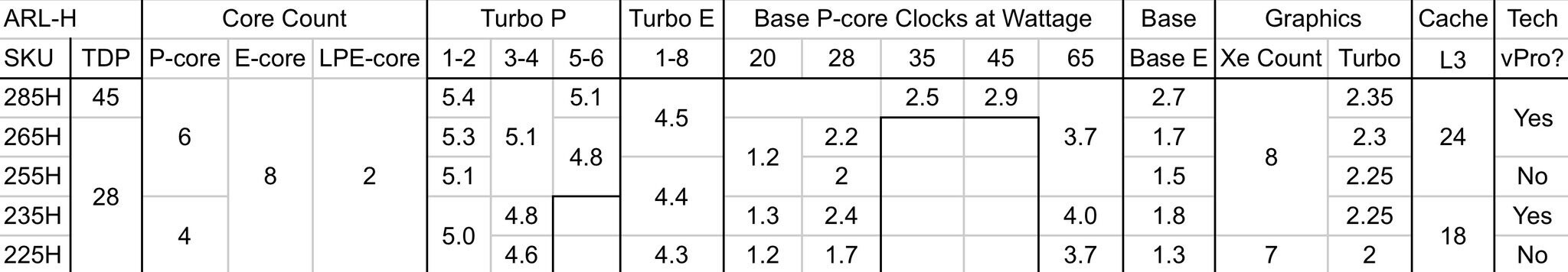
As we await the launch of Intel's "Arrow Lake-S" Core Ultra 200S series of processors for desktops, we are getting some new leaks about Intel's mainstream mobile "Arrow Lake-H" update. A month ago, we got the specification table of the high-end mobile "Arrow Lake-HX," and now, thanks to Jaykihn X, we have the mainstream laptop chip specifications as well. The top-of-the-line includes Intel Core Ultra 9 285H, a 45 W TDP SKU with six P-cores, eight E-cores, and two LPE cores. The CPU packs integrated Xe2 graphics with eight cores and 24 MB of total L3 cache and has a maximum boost of 5.4 GHz for P-cores.
Moving down the stack, there are Core Ultra 7 265H and Core Ultra 5 255H SKUs, which feature the same P/E/LPE core configuration. However, these SKUs are rated for 28 W TDP, having lower maximum frequencies and the same iGPU configuration. This time, we also have two Core Ultra 3 SKUs, with Core Ultra 3 235H and 225H bringing four P-cores, eight E-cores, and two LPE-cores in the 28 W package. The Core Ultra 3 235H has eight Xe2 cores in its iGPU, while the lowest-end Core Ultra 3 225H has only seven Xe2 iGPU cores. For a complete set of specifications, including all clock speeds in base and boost, please check out the table below.
Moving down the stack, there are Core Ultra 7 265H and Core Ultra 5 255H SKUs, which feature the same P/E/LPE core configuration. However, these SKUs are rated for 28 W TDP, having lower maximum frequencies and the same iGPU configuration. This time, we also have two Core Ultra 3 SKUs, with Core Ultra 3 235H and 225H bringing four P-cores, eight E-cores, and two LPE-cores in the 28 W package. The Core Ultra 3 235H has eight Xe2 cores in its iGPU, while the lowest-end Core Ultra 3 225H has only seven Xe2 iGPU cores. For a complete set of specifications, including all clock speeds in base and boost, please check out the table below.

Samsung's 5 nm Node in Production, First SoCs to Arrive Soon
During its Q3 earnings call, Samsung Electronics has provided everyone with an update on its foundry and node production development. In the past year or so, Samsung's foundry has been a producer of a 7 nm LPP (Low Power Performance) node as its smallest node. That is now changed as Samsung has started the production of the 5 nm LPE (Low Power Early) semiconductor manufacturing node. In the past, we have reported that the company struggled with yields of its 5 nm process, however, that seems to be ironed out and now the node is in full production. To contribute to the statement that the new node is doing well, we also recently reported that Samsung will be the sole manufacturer of Qualcomm Snapdragon 875 5G SoC.
The new 5 nm semiconductor node is a marginal improvement over the past 7 nm node. It features a 10% performance improvement that is taking the same power and chip complexity or a 20% power reduction of the same processor clocks and design. When it comes to density, the company advertises the node with x1.33 times increase in transistor density compared to the previous node. The 5LPE node is manufactured using the Extreme Ultra-Violet (EUV) methodology and its FinFET transistors feature new characteristics like Smart Difusion Break isolation, flexible contact placement, and single-fin devices for low power applications. The node is design-rule compatible with the previous 7 nm LPP node, so the existing IP can be used and manufactured on this new process. That means that this is not a brand new process but rather an enhancement. First products are set to arrive with the next generation of smartphone SoCs, like the aforementioned Qualcomm Snapdragon 875.
The new 5 nm semiconductor node is a marginal improvement over the past 7 nm node. It features a 10% performance improvement that is taking the same power and chip complexity or a 20% power reduction of the same processor clocks and design. When it comes to density, the company advertises the node with x1.33 times increase in transistor density compared to the previous node. The 5LPE node is manufactured using the Extreme Ultra-Violet (EUV) methodology and its FinFET transistors feature new characteristics like Smart Difusion Break isolation, flexible contact placement, and single-fin devices for low power applications. The node is design-rule compatible with the previous 7 nm LPP node, so the existing IP can be used and manufactured on this new process. That means that this is not a brand new process but rather an enhancement. First products are set to arrive with the next generation of smartphone SoCs, like the aforementioned Qualcomm Snapdragon 875.

Apr 16th, 2025 08:53 EDT
change timezone
Latest GPU Drivers
New Forum Posts
- Last game you purchased? (771)
- GPU Memory Temprature is always high (16)
- Windows 11 fresh install to do list (20)
- 5070ti overclock...what are your settings? (3)
- Help For XFX RX 590 GME Chinese - Vbios (4)
- PCGH: "hidden site" to see total money spend on steam (3)
- Share your AIDA 64 cache and memory benchmark here (3053)
- NVFlash for RTX 50 Series (Blackwell) (0)
- intel 1700 with high speed ram,memory (63)
- The TPU UK Clubhouse (26115)
Popular Reviews
- G.SKILL Trident Z5 NEO RGB DDR5-6000 32 GB CL26 Review - AMD EXPO
- ASUS GeForce RTX 5080 TUF OC Review
- DAREU A950 Wing Review
- The Last Of Us Part 2 Performance Benchmark Review - 30 GPUs Compared
- Sapphire Radeon RX 9070 XT Pulse Review
- Sapphire Radeon RX 9070 XT Nitro+ Review - Beating NVIDIA
- Upcoming Hardware Launches 2025 (Updated Apr 2025)
- Thermaltake TR100 Review
- Zotac GeForce RTX 5070 Ti Amp Extreme Review
- TerraMaster F8 SSD Plus Review - Compact and quiet
Controversial News Posts
- NVIDIA GeForce RTX 5060 Ti 16 GB SKU Likely Launching at $499, According to Supply Chain Leak (182)
- NVIDIA Sends MSRP Numbers to Partners: GeForce RTX 5060 Ti 8 GB at $379, RTX 5060 Ti 16 GB at $429 (124)
- Nintendo Confirms That Switch 2 Joy-Cons Will Not Utilize Hall Effect Stick Technology (105)
- Over 200,000 Sold Radeon RX 9070 and RX 9070 XT GPUs? AMD Says No Number was Given (100)
- Nintendo Switch 2 Launches June 5 at $449.99 with New Hardware and Games (99)
- Sony Increases the PS5 Pricing in EMEA and ANZ by Around 25 Percent (85)
- NVIDIA PhysX and Flow Made Fully Open-Source (77)
- NVIDIA Pushes GeForce RTX 5060 Ti Launch to Mid-April, RTX 5060 to May (77)