Apr 16th, 2025 09:18 EDT
change timezone
Latest GPU Drivers
New Forum Posts
- Last game you purchased? (772)
- Help me identify Chip of this DDR4 RAM (20)
- 5070ti overclock...what are your settings? (5)
- Windows 11 fresh install to do list (23)
- How to relubricate a fan and/or service a troublesome/noisy fan. (229)
- GPU Memory Temprature is always high (16)
- Help For XFX RX 590 GME Chinese - Vbios (4)
- PCGH: "hidden site" to see total money spend on steam (3)
- Share your AIDA 64 cache and memory benchmark here (3053)
- NVFlash for RTX 50 Series (Blackwell) (0)
Popular Reviews
- G.SKILL Trident Z5 NEO RGB DDR5-6000 32 GB CL26 Review - AMD EXPO
- ASUS GeForce RTX 5080 TUF OC Review
- DAREU A950 Wing Review
- The Last Of Us Part 2 Performance Benchmark Review - 30 GPUs Compared
- Sapphire Radeon RX 9070 XT Pulse Review
- Sapphire Radeon RX 9070 XT Nitro+ Review - Beating NVIDIA
- Upcoming Hardware Launches 2025 (Updated Apr 2025)
- Thermaltake TR100 Review
- Zotac GeForce RTX 5070 Ti Amp Extreme Review
- TerraMaster F8 SSD Plus Review - Compact and quiet
Controversial News Posts
- NVIDIA GeForce RTX 5060 Ti 16 GB SKU Likely Launching at $499, According to Supply Chain Leak (182)
- NVIDIA Sends MSRP Numbers to Partners: GeForce RTX 5060 Ti 8 GB at $379, RTX 5060 Ti 16 GB at $429 (124)
- Nintendo Confirms That Switch 2 Joy-Cons Will Not Utilize Hall Effect Stick Technology (105)
- Over 200,000 Sold Radeon RX 9070 and RX 9070 XT GPUs? AMD Says No Number was Given (100)
- Nintendo Switch 2 Launches June 5 at $449.99 with New Hardware and Games (99)
- Sony Increases the PS5 Pricing in EMEA and ANZ by Around 25 Percent (85)
- NVIDIA PhysX and Flow Made Fully Open-Source (77)
- NVIDIA Pushes GeForce RTX 5060 Ti Launch to Mid-April, RTX 5060 to May (77)
News Posts matching #R&D
Return to Keyword Browsing
ASML Reports €7.7 Billion Total Net Sales and €2.4 Billion Net Income in Q1 2025
Today, ASML Holding NV (ASML) has published its 2025 first-quarter results.
"Our first-quarter total net sales came in at €7.7 billion, in line with our guidance. The gross margin was 54.0%, above guidance, driven by a favorable EUV product mix and the achievement of performance milestones. In the first quarter, we shipped our fifth High NA system, and we now have these systems at three customers. Our conversations so far with customers support our expectation that 2025 and 2026 will be growth years. However, the recent tariff announcements have increased uncertainty in the macro environment and the situation will remain dynamic for a while. As previously shared, artificial intelligence continues to be the primary growth driver in our industry. It has created a shift in the market dynamics that benefits some customers more than others, contributing to both upside potential and downside risks as reflected in our 2025 revenue range.
- Q1 total net sales of €7.7 billion, gross margin of 54.0%, net income of €2.4 billion
- Quarterly net bookings in Q1 of €3.9 billion f which €1.2 billion is EUV
- ASML expects Q2 2025 total net sales between €7.2 billion and €7.7 billion, and a gross margin between 50% and 53%
- ASML continues to expect 2025 total net sales to be between €30 billion and €35 billion, with a gross margin between 51% and 53%
"Our first-quarter total net sales came in at €7.7 billion, in line with our guidance. The gross margin was 54.0%, above guidance, driven by a favorable EUV product mix and the achievement of performance milestones. In the first quarter, we shipped our fifth High NA system, and we now have these systems at three customers. Our conversations so far with customers support our expectation that 2025 and 2026 will be growth years. However, the recent tariff announcements have increased uncertainty in the macro environment and the situation will remain dynamic for a while. As previously shared, artificial intelligence continues to be the primary growth driver in our industry. It has created a shift in the market dynamics that benefits some customers more than others, contributing to both upside potential and downside risks as reflected in our 2025 revenue range.


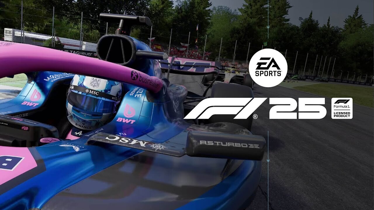
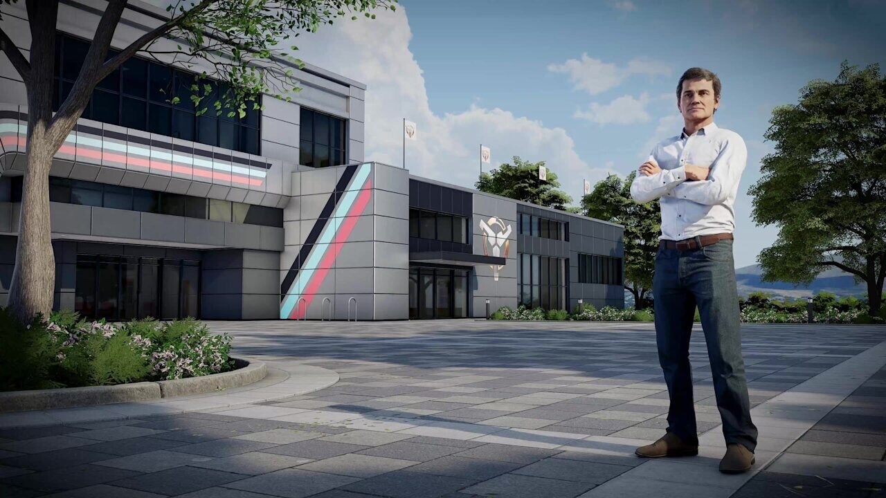
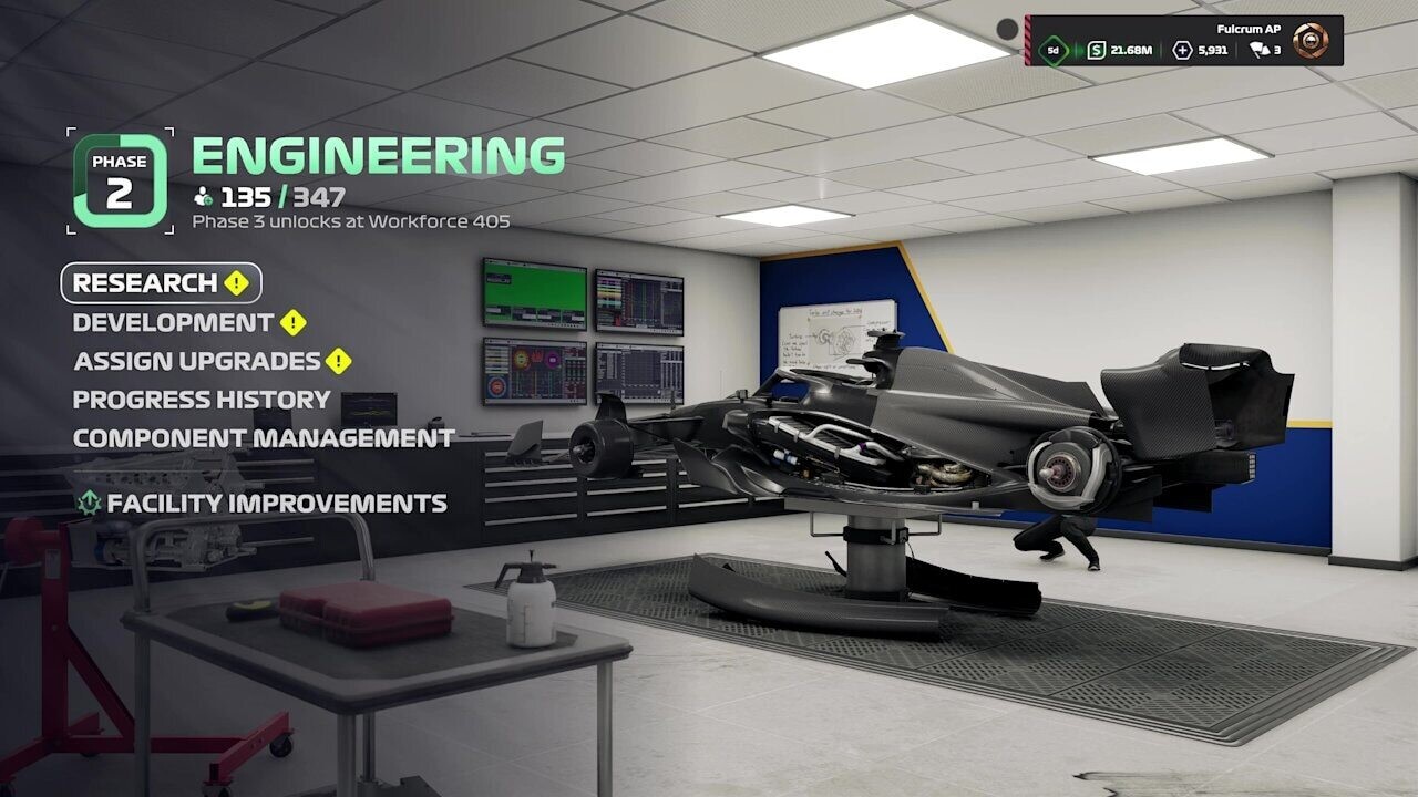
EA Sports Dives Deep into F1 25's Revamped My Team & Driver Career Modes
Introducing My Team 2.0: as mentioned as part of our Reveal, My Team is having its biggest overhaul since it was introduced in F1 2020. If you've played My Team in one of our previous F1 games, you'll be familiar with taking on the role of driver/owner, a single character that not only runs the day-to-day activities behind the scenes, but also jumps into the cockpit for the on-track action. For F1 25 however, we're shaking things up, as My Team 2.0 sees you take on a more authentic, management-focused role in that of a team owner.
In addition to handling day-to-day running of the critical facilities that make an F1 team tick such as Engineering, Personnel and Corporate, you'll be responsible for recruiting and managing a pair of drivers to represent your team. Then, during race weekends, you'll be given the choice as to which driver you'd like to take to the track. By managing the competing concerns of two drivers instead of just a single teammate, you'll discover what kind of owner you'd like to be. We believe this refreshed approach allows you to craft a My Team story that's unique to you, unlocking new avenues of decision-making for you to explore.


In addition to handling day-to-day running of the critical facilities that make an F1 team tick such as Engineering, Personnel and Corporate, you'll be responsible for recruiting and managing a pair of drivers to represent your team. Then, during race weekends, you'll be given the choice as to which driver you'd like to take to the track. By managing the competing concerns of two drivers instead of just a single teammate, you'll discover what kind of owner you'd like to be. We believe this refreshed approach allows you to craft a My Team story that's unique to you, unlocking new avenues of decision-making for you to explore.


Tokyo Electron & IBM Renew Collaboration for Advanced Semiconductor Technology
This week, IBM and Tokyo Electron (TEL) announced an extension of their agreement for the joint research and development of advanced semiconductor technologies. The new 5-year agreement will focus on the continued advancement of technology for next-generation semiconductor nodes and architectures to power the age of generative AI. This agreement builds on a more than two-decade partnership between IBM and TEL for joint research and development. Previously, the two companies have achieved several breakthroughs, including the development of a new laser debonding process for producing 300 mm silicon chip wafers for 3D chip stacking technology.
Now, bringing together IBM's expertise in semiconductor process integration and TEL's leading-edge equipment, they will explore technology for smaller nodes and chiplet architectures to achieve the performance and energy efficiency requirements for the future of generative AI. "The work IBM and TEL have done together over the last 20 years has helped to push the semiconductor technology innovation to provide many generations of chip performance and energy efficiency to the semiconductor industry," said Mukesh Khare, GM of IBM Semiconductors and VP of Hybrid Cloud, IBM. "We are thrilled to be continuing our work together at this critical time to accelerate chip innovations that can fuel the era of generative AI."


Now, bringing together IBM's expertise in semiconductor process integration and TEL's leading-edge equipment, they will explore technology for smaller nodes and chiplet architectures to achieve the performance and energy efficiency requirements for the future of generative AI. "The work IBM and TEL have done together over the last 20 years has helped to push the semiconductor technology innovation to provide many generations of chip performance and energy efficiency to the semiconductor industry," said Mukesh Khare, GM of IBM Semiconductors and VP of Hybrid Cloud, IBM. "We are thrilled to be continuing our work together at this critical time to accelerate chip innovations that can fuel the era of generative AI."


Quantum Machines Anticipates Collaborative Breakthroughs at NVIDIA's New Research Center
Quantum Machines (QM), a leading provider of advanced quantum control solutions, today announced its intention to work with NVIDIA at its newly established NVIDIA Accelerated Quantum Research Center (NVAQC), unveiled at the GTC global AI conference. The Boston-based center aims to advance quantum computing research with accelerated computing, including integrating quantum processors with AI- supercomputing to overcome significant challenges in the quantum computing space. As quantum computing rapidly evolves, the integration of quantum processors with powerful AI supercomputers becomes increasingly essential. These accelerated quantum supercomputers are pivotal for advancing quantum error correction, device control, and algorithm development.
Quantum Machines joins other quantum computing pioneers, including Quantinuum and QuEra, along with academic partners from Harvard and MIT, in working with NVIDIA at the NVAQC to develop pioneering research. Quantum Machines will work with NVIDIA to integrate its NVIDIA GB200 Grace Blackwell Superchips with QM's advanced quantum control technologies, including the OPX1000. This integration will facilitate rapid, high-bandwidth communication between quantum processors and classical supercomputers. QM and NVIDIA thereby lay the essential foundations for quantum error correction and robust quantum algorithm execution. By reducing latency and enhancing processing efficiency, QM and NVIDIA solutions will significantly accelerate practical applications of quantum computing.


Quantum Machines joins other quantum computing pioneers, including Quantinuum and QuEra, along with academic partners from Harvard and MIT, in working with NVIDIA at the NVAQC to develop pioneering research. Quantum Machines will work with NVIDIA to integrate its NVIDIA GB200 Grace Blackwell Superchips with QM's advanced quantum control technologies, including the OPX1000. This integration will facilitate rapid, high-bandwidth communication between quantum processors and classical supercomputers. QM and NVIDIA thereby lay the essential foundations for quantum error correction and robust quantum algorithm execution. By reducing latency and enhancing processing efficiency, QM and NVIDIA solutions will significantly accelerate practical applications of quantum computing.


Qualcomm Announces Acquisition of VinAI Division, Aims to Expand GenAI Capabilities
Qualcomm today announced the acquisition of MovianAI Artificial Intelligence (AI) Application and Research JSC (MovianAI), the former generative AI division of VinAI Application and Research JSC (VinAI) and a part of the Vingroup ecosystem. As a leading AI research company, VinAI is renowned for its expertise in generative AI, machine learning, computer vision, and natural language processing. Combining VinAI's advanced generative AI research and development (R&D) capabilities with Qualcomm's decades of extensive R&D will expand its ability to drive extraordinary inventions.
For more than 20 years, Qualcomm has been working closely with the Vietnamese technology ecosystem to create and deliver innovative solutions. Qualcomm's innovations in the areas of 5G, AI, IoT and automotive have helped to fuel the extraordinary growth and success of Vietnam's information and communication technology (ICT) industry and assisted the entry of Vietnamese companies into the global marketplace.

For more than 20 years, Qualcomm has been working closely with the Vietnamese technology ecosystem to create and deliver innovative solutions. Qualcomm's innovations in the areas of 5G, AI, IoT and automotive have helped to fuel the extraordinary growth and success of Vietnam's information and communication technology (ICT) industry and assisted the entry of Vietnamese companies into the global marketplace.


Intel to Receive $1.9 Billion as SK Hynix Finalizes NAND Deal
Intel and SK Hynix have finalized an $8.85 billion transaction involving Intel's NAND flash memory operations, marking the conclusion of a two-phase deal initiated in 2020. In the first phase of the transaction, SK Hynix acquired Intel's SSD division along with a NAND production facility in Dalian, China, for $6.61 billion. The Dalian facility was later rebranded as Solidigm. Notably, this phase transferred only the physical assets and operational facilities, leaving behind critical intellectual property, research and development infrastructure, and specialized technical staff. The second phase, finalized with a payment of $1.9 billion this Tuesday, addressed these remaining components. With this payment, SK Hynix secured full rights to Intel's proprietary NAND technology, R&D resources, and the technical workforce dedicated to NAND operations.
During the transition period, Intel maintained control over these elements, which limited integration between Solidigm and Intel's NAND teams. This separation was designed to manage operational risks and gradually transfer capabilities. Completing this deal helps with a strategic restructuring of Intel's portfolio as it shifts focus toward high-growth areas such as AI chip development, foundry services, and next-generation semiconductor manufacturing. A $1.9 billion financial injection is perfect in time for Intel Foundry business, burning billions per year, to offset some of the losses. For SK Hynix, consolidating the complete range of Intel's NAND operations enhances its competitive position in the global NAND market, providing access to established technologies and key industry expertise. This finalization is part of a broader trend where companies divest from commoditized memory products to concentrate on more advanced semiconductor solutions like AI chips and other accelerators, which are enjoying higher margins and a better business outlook.
During the transition period, Intel maintained control over these elements, which limited integration between Solidigm and Intel's NAND teams. This separation was designed to manage operational risks and gradually transfer capabilities. Completing this deal helps with a strategic restructuring of Intel's portfolio as it shifts focus toward high-growth areas such as AI chip development, foundry services, and next-generation semiconductor manufacturing. A $1.9 billion financial injection is perfect in time for Intel Foundry business, burning billions per year, to offset some of the losses. For SK Hynix, consolidating the complete range of Intel's NAND operations enhances its competitive position in the global NAND market, providing access to established technologies and key industry expertise. This finalization is part of a broader trend where companies divest from commoditized memory products to concentrate on more advanced semiconductor solutions like AI chips and other accelerators, which are enjoying higher margins and a better business outlook.

Semiconductor Industry Calls for Stronger European Strategy
Seeking to explore semiconductor policy measures that can strengthen the industrial policy in the European Union, SEMI and the European Semiconductor Industry Association (ESIA) have successfully held a high-level roundtable event in the European Parliament under the auspices of Members of the European Parliament (MEPs) Bart Groothuis (Renew Europe), Oliver Schenk (European People's Party) and Dan Nica (Socialists and Democrats Party).
The 2023 European Chips Act marked an important milestone for Europe's semiconductor industry and overall industrial ecosystem, providing concrete measures to enhance competitiveness and technological capabilities. In order to build on the success of the Chips Act, after the roundtable, MEPs signed a joint declaration to the European Commission's Executive Vice President for Tech Sovereignty, Security and Democracy, Henna Virkkunen, calling for an ambitious follow-up to the Chips Act that adds new research and development (R&D) funds, attracts new investments, and increases European competitiveness.
The 2023 European Chips Act marked an important milestone for Europe's semiconductor industry and overall industrial ecosystem, providing concrete measures to enhance competitiveness and technological capabilities. In order to build on the success of the Chips Act, after the roundtable, MEPs signed a joint declaration to the European Commission's Executive Vice President for Tech Sovereignty, Security and Democracy, Henna Virkkunen, calling for an ambitious follow-up to the Chips Act that adds new research and development (R&D) funds, attracts new investments, and increases European competitiveness.


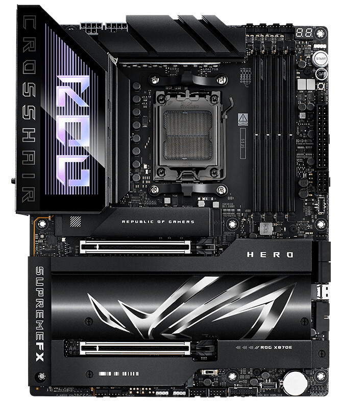
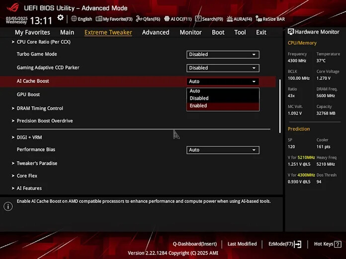
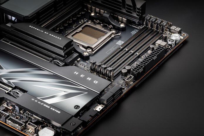
ASUS Introduces New "AI Cache Boost" BIOS Feature - R&D Team Claims Performance Uplift
Large language models (LLMs) love large quantities of memory—so much so, in fact, that AI enthusiasts are turning to multi-GPU setups to make even more VRAM available for their AI apps. But since many current LLMs are extremely large, even this approach has its limits. At times, the GPU will decide to make use of CPU processing power for this data, and when it does, the performance of your CPU cache and DRAM comes into play. All this means that when it comes to the performance of AI applications, it's not just the GPU that matters, but the entire pathway that connects the GPU to the CPU to the I/O die to the DRAM modules. It stands to reason, then, that there are opportunities to boost AI performance by optimizing these elements.
That's exactly what we've found as we've spent time in our R&D labs with the latest AMD Ryzen CPUs. AMD just launched two new Ryzen CPUs with AMD 3D V-Cache Technology, the AMD Ryzen 9 9950X3D and Ryzen 9 9900X3D, pushing the series into new performance territory. After testing a wide range of optimizations in a variety of workloads, we uncovered a range of settings that offer tangible benefits for AI enthusiasts. Now, we're ready to share these optimizations with you through a new BIOS feature: AI Cache Boost. Available through an ASUS AMD 800 Series motherboard and our most recent firmware update, AI Cache Boost can accelerate performance up to 12.75% when you're working with massive LLMs.


That's exactly what we've found as we've spent time in our R&D labs with the latest AMD Ryzen CPUs. AMD just launched two new Ryzen CPUs with AMD 3D V-Cache Technology, the AMD Ryzen 9 9950X3D and Ryzen 9 9900X3D, pushing the series into new performance territory. After testing a wide range of optimizations in a variety of workloads, we uncovered a range of settings that offer tangible benefits for AI enthusiasts. Now, we're ready to share these optimizations with you through a new BIOS feature: AI Cache Boost. Available through an ASUS AMD 800 Series motherboard and our most recent firmware update, AI Cache Boost can accelerate performance up to 12.75% when you're working with massive LLMs.

Google Teams up with MediaTek for Next-Generation TPU v7 Design
According to Reuters, citing The Information, Google will collaborate with MediaTek to develop its seventh-generation Tensor Processing Unit (TPU), which is also known as TPU v7. Google maintains its existing partnership with Broadcom despite the new MediaTek collaboration. The AI accelerator is scheduled for production in 2026, and TSMC is handling manufacturing duties. Google will lead the core architecture design while MediaTek manages I/O and peripheral components, as Economic Daily News reports. This differs from Google's ongoing relationship with Broadcom, which co-develops core TPU architecture. The MediaTek partnership reportedly stems from the company's strong TSMC relationship and lower costs compared to Broadcom.
There is also a possibility that MediaTek could design inference-focused TPU v7 chips while Broadcom focuses on training architecture. Nonetheless, the development of TPU is a massive market as Google is using so many chips that it could use a third company, hypothetically. The development of TPU continues Google's vertical integration strategy for AI infrastructure. Google reduces dependency on NVIDIA hardware by designing proprietary AI chips for internal R&D and cloud operations. At the same time, competitors like OpenAI, Anthropic, and Meta rely heavily on NVIDIA's processors for AI training and inference. At Google's scale, serving billions of queries a day, designing custom chips makes sense from both financial and technological sides. As Google develops its own specific workloads, translating that into hardware acceleration is the game that Google has been playing for years now.
There is also a possibility that MediaTek could design inference-focused TPU v7 chips while Broadcom focuses on training architecture. Nonetheless, the development of TPU is a massive market as Google is using so many chips that it could use a third company, hypothetically. The development of TPU continues Google's vertical integration strategy for AI infrastructure. Google reduces dependency on NVIDIA hardware by designing proprietary AI chips for internal R&D and cloud operations. At the same time, competitors like OpenAI, Anthropic, and Meta rely heavily on NVIDIA's processors for AI training and inference. At Google's scale, serving billions of queries a day, designing custom chips makes sense from both financial and technological sides. As Google develops its own specific workloads, translating that into hardware acceleration is the game that Google has been playing for years now.
China Dedicates $55 Billion for Semiconductor, AI, and Quantum Computing Development in 2025
China's Ministry of Finance has allocated $55 billion (¥398.12 billion) for science and technology funding in 2025, marking a 10% increase from the previous year's $50 billion (¥361.9 billion). This expenditure now stands as the nation's third-largest budget item, following only national defense and debt interest payments. The 2024 allocation achieved a 97.6% implementation rate, indicating effective deployment of resources in the technology sector. The funding prioritizes initiatives under the "Science and Technology Innovation 2030" program, with significant investments targeting semiconductors, artificial intelligence, and quantum computing research. Rather than stimulating immediate breakthroughs, the incremental funding increase aims to strengthen existing projects and enhance technological self-reliance amid global competition.
This strategy shows some fiscal constraints imposed by China's economic slowdown while maintaining the country's long-term technological objectives. Supplementary measures bolster direct R&D investment, including enhanced support for fundamental research and specialized financing mechanisms for technology-focused enterprises. Tax reductions and targeted subsidies form part of a comprehensive policy framework designed to foster domestic innovation capabilities. While the funding increase shows commitment to technological advancement, effective project management and efficient resource allocation will be critical success factors, mainly as China competes more globally. Perhaps the most important milestone for this aid package will be supporting the development of advanced lithography tools to make sure that domestic companies can manufacture cutting-edge silicon.
This strategy shows some fiscal constraints imposed by China's economic slowdown while maintaining the country's long-term technological objectives. Supplementary measures bolster direct R&D investment, including enhanced support for fundamental research and specialized financing mechanisms for technology-focused enterprises. Tax reductions and targeted subsidies form part of a comprehensive policy framework designed to foster domestic innovation capabilities. While the funding increase shows commitment to technological advancement, effective project management and efficient resource allocation will be critical success factors, mainly as China competes more globally. Perhaps the most important milestone for this aid package will be supporting the development of advanced lithography tools to make sure that domestic companies can manufacture cutting-edge silicon.


Scientists Cast Doubt on Microsoft's Quantum "Breakthrough" with Majorana 1 Chip
Microsoft launched its Majorana 1 chip—the world's first quantum processor powered by a Topological Core architecture—last month. The company's debuting of its Majorana design was celebrated as a significant milestone—in 2023, an ambitious roadmap was published by Microsoft's research department. At the time, a tall Majorana particle-based task was set: the building of a proprietary quantum supercomputer within a decade. Returning to the present day; outside parties have criticized Microsoft's February announcements. The Register published an investigative piece earlier today, based on quotes from key players specializing in the field of Quantum studies. Many propose a theoretical existence of Majorana particles, while Microsoft R&D employees have claimed detection and utilization. The Register referred back to recent history: "(Microsoft) made big claims about Majorana particles before, but it didn't end well: in 2021 Redmond's researchers retracted a 2018 paper in which they claimed to have detected the particles."
As pointed out by Microsoft researcher Chetan Nayak; their latest paper was actually authored last March 2024, but only made public in recent weeks. Further details of progress are expected next week, at the American Physical Society (APS) 2025 Joint March Meeting. The Register has compiled quotes from vocal critics; starting with Henry Legg—a lecturer in theoretical physics at the University of St Andrews, Scotland. The noted scholar believes—as divulged in a scientific online comment—that Microsoft's claimed Quantum breakthrough: "is not reliable and must be revisited." Similarly, collaborators from Germany's Forschungszentrum Jülich institute and the University of Pittsburgh, USA released a joint video statement. (Respectively) Experimental physicist Vincent Mourik and by Professor Sergey Frolov outlined: "distractions caused by unreliable scientific claims from Microsoft Quantum."


As pointed out by Microsoft researcher Chetan Nayak; their latest paper was actually authored last March 2024, but only made public in recent weeks. Further details of progress are expected next week, at the American Physical Society (APS) 2025 Joint March Meeting. The Register has compiled quotes from vocal critics; starting with Henry Legg—a lecturer in theoretical physics at the University of St Andrews, Scotland. The noted scholar believes—as divulged in a scientific online comment—that Microsoft's claimed Quantum breakthrough: "is not reliable and must be revisited." Similarly, collaborators from Germany's Forschungszentrum Jülich institute and the University of Pittsburgh, USA released a joint video statement. (Respectively) Experimental physicist Vincent Mourik and by Professor Sergey Frolov outlined: "distractions caused by unreliable scientific claims from Microsoft Quantum."


SteelSeries Introduces QcK Performance Mousepad Series
Precision made personal—introducing the QcK Performance Series, our first premium mousepad collection crafted to sync seamlessly with your unique playstyle. Your gameplay is personal, and now your surface can be too. Friction or Glide? You decide. Extra density. Extra consistency. High-grade neoprene foam creates a stable foundation for your mouse to move at high speeds with no sensor skip, round in, round out.
QcK Evolves Again
Introducing the next evolution in gaming—QcK Performance, the first family of performance mousepads engineered with one goal in mind: to elevate your gameplay. Developed in collaboration with top esports athletes, QcK Performance offers three meticulously crafted and unique surfaces: Speed, Balance and Control. Whatever your playstyle, discover the ultimate surface to push your performance to the next level.


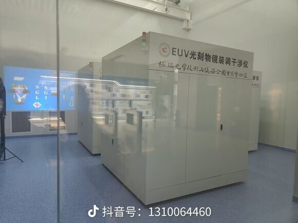
China Develops Domestic EUV Tool, ASML Monopoly in Trouble
China's domestic extreme ultraviolet (EUV) lithography development is far from a distant dream. The newest system, now undergoing testing at Huawei's Dongguan facility, leverages laser-induced discharge plasma (LDP) technology, representing a potentially disruptive approach to EUV light generation. The system is scheduled for trial production in Q3 2025, with mass manufacturing targeted for 2026, potentially positioning China to break ASML's technical monopoly in advanced lithography. The LDP approach employed in the Chinese system generates 13.5 nm EUV radiation by vaporizing tin between electrodes and converting it to plasma via high-voltage discharge, where electron-ion collisions produce the required wavelength. This methodology offers several technical advantages over ASML's laser-produced plasma (LPP) technique, including simplified architecture, reduced footprint, improved energy efficiency, and potentially lower production costs.
The LPP method relies on high-energy lasers and complex FPGA-based real-time control electronics to achieve the same result. While ASML has refined its LPP-based systems over decades, the inherent efficiency advantages of the LDP approach could accelerate China's catch-up timeline in this critical semiconductor manufacturing technology. When the US imposed sanctions on EUV shipments to Chinese companies, the Chinese semiconductor development was basically limited as standard deep ultraviolet (DUV) wave lithography systems utilize 248 nm (KrF) and 193 nm (ArF) wavelengths for semiconductor patterning, with 193 nm immersion technology representing the most advanced pre-EUV production technique. These longer wavelengths contrast with EUV's 13.5 nm radiation, requiring multiple patterning techniques to achieve advanced nodes.

The LPP method relies on high-energy lasers and complex FPGA-based real-time control electronics to achieve the same result. While ASML has refined its LPP-based systems over decades, the inherent efficiency advantages of the LDP approach could accelerate China's catch-up timeline in this critical semiconductor manufacturing technology. When the US imposed sanctions on EUV shipments to Chinese companies, the Chinese semiconductor development was basically limited as standard deep ultraviolet (DUV) wave lithography systems utilize 248 nm (KrF) and 193 nm (ArF) wavelengths for semiconductor patterning, with 193 nm immersion technology representing the most advanced pre-EUV production technique. These longer wavelengths contrast with EUV's 13.5 nm radiation, requiring multiple patterning techniques to achieve advanced nodes.


Giga Computing, SK Telecom, and SK Enmove to Collaborate on AI Data Center Liquid Cooling Technology
Giga Computing, a subsidiary of GIGABYTE Technology, has signed a Memorandum of Understanding (MoU) with SK Telecom and SK Enmove to collaborate on advancing AI Data Center (AIDC) and high-performance computing (HPC) while accelerating the adoption of liquid cooling technology in next-generation data centers.
This strategic partnership sets the stage to nurture and develop high-performance, energy-efficient, and sustainable data center solutions.
Driving AI and Cooling Technology Innovation Together
Performance AI servers, liquid cooling technologies, and modular AI clusters to support SK's various business units, including:
- SK Telecom: Strengthening AIDC infrastructure to support next-generation data centers
- SK Enmove: Advancing liquid cooling technologies to improve energy efficiency and sustainability in data centers


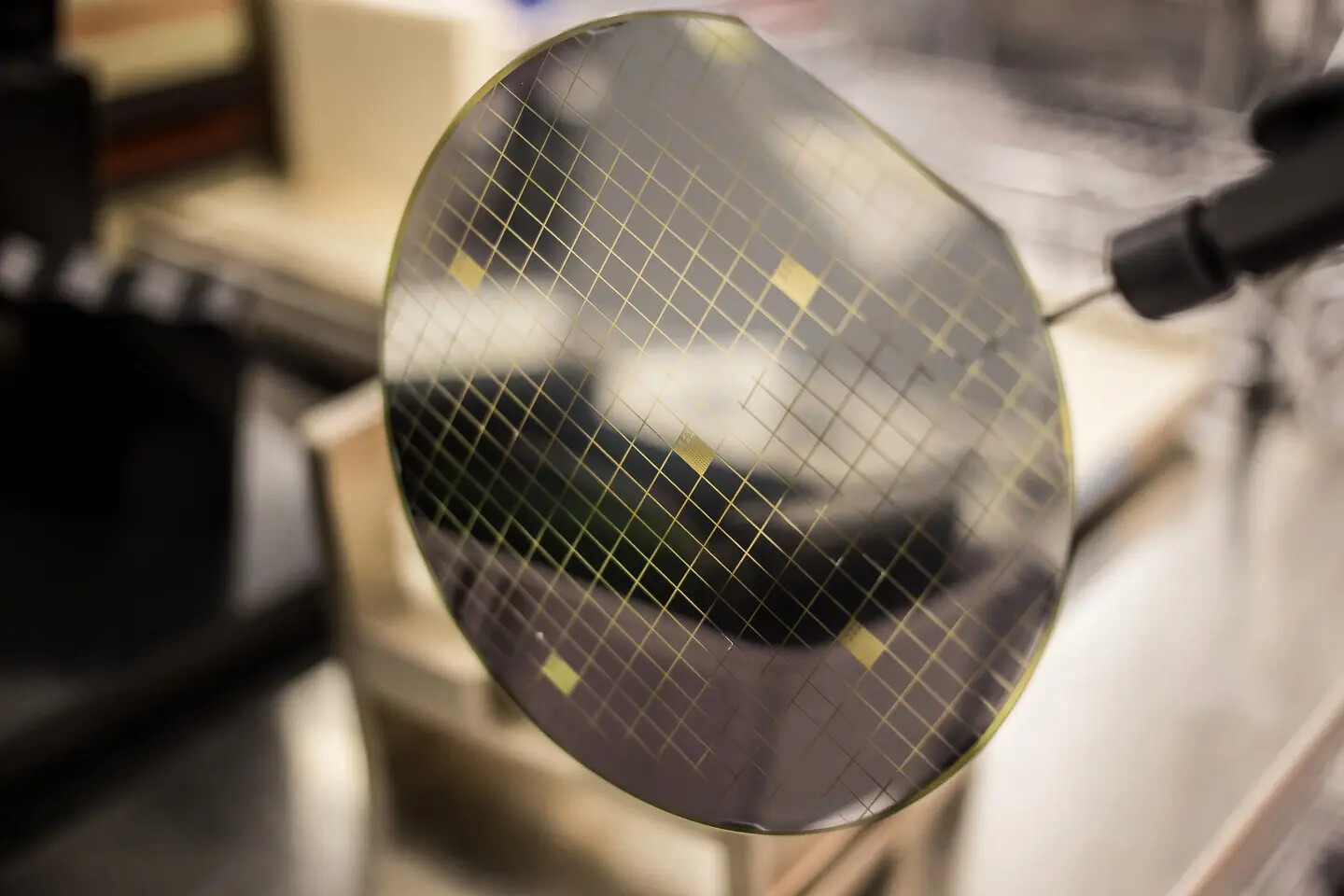
Alibaba Adds New "C930" Server-grade Chip to XuanTie RISC-V Processor Series
Damo Academy—a research and development wing of Alibaba—launched its debut "server-grade processor" design late last week, in Beijing. According to a South China Morning Post (SCMP) news article, the C930 model is a brand-new addition to the e-commerce platform's XuanTie RISC-V CPU series. Company representatives stated that their latest product is designed as a server-level and high-performance computing (HPC) solution. Going back to March 2024, TechPowerUp and other Western hardware news outlets picked up on Alibaba's teasing of the Xuantie C930 SoC, and a related Xuantie 907 matrix processing unit. Fast-forward to the present day; Damo Academy has disclosed that initial shipments—of finalized C930 units—will be sent out to customers this month.
The newly released open-source RISC-V architecture-based HPC chip is an unknown quantity in terms of technical specifications. Damo Academy reps did not provide any detailed information during last Friday's conference (February 28). SCMP's report noted the R&D division's emphasizing of "its role in advancing RISC-V adoption" within various high-end fields. Apparently, the XuanTie engineering team has: "supported the implementation of more than thirty percent of RISC-V high-performance processors." Upcoming additions will arrive in the form of the C908X for AI acceleration, R908A for automotive processing solutions, and an XL200 model for high-speed interconnection. These XuanTie projects are reportedly still deep in development.


The newly released open-source RISC-V architecture-based HPC chip is an unknown quantity in terms of technical specifications. Damo Academy reps did not provide any detailed information during last Friday's conference (February 28). SCMP's report noted the R&D division's emphasizing of "its role in advancing RISC-V adoption" within various high-end fields. Apparently, the XuanTie engineering team has: "supported the implementation of more than thirty percent of RISC-V high-performance processors." Upcoming additions will arrive in the form of the C908X for AI acceleration, R908A for automotive processing solutions, and an XL200 model for high-speed interconnection. These XuanTie projects are reportedly still deep in development.


Chinese Mature Nodes Undercut Western Silicon Pricing, to Capture up to 28% of the Market This Year
Chinese manufacturers have seized significant market share in legacy chip production, driving prices down and creating intense competitive pressure that Western competitors cannot match. The so-called "China shock" in the semiconductor sector appears as mature node production shifts East at accelerating rates. Legacy process nodes, which are usually 16/20/22/24 nm and larger, form the backbone of consumer electronics and automotive applications while providing established manufacturers with stable revenue streams for R&D investment. However, this economic framework now faces structural disruption as Chinese fabs leverage domestic demand and government support to expand capacity. By Q4 2025, Chinese facilities will control 28% of global mature chip production, with projections indicating further expansion to 39% by 2027.
This rapid capacity growth directly results from Beijing's strategic pivot following US export controls on advanced semiconductor equipment, which redirected investment toward mature nodes where technological barriers remain lower. This is happening in parallel with companies like SMIC, although isolated, which are developing lithography solutions for cutting-edge 5 nm and 3 nm wafer production. For older nodes, The market impact appears most pronounced in specialized materials like silicon carbide (SiC). Industry benchmark 6-inch SiC wafers from Wolfspeed were previously $1,500, compared to current $500 pricing from Guangzhou Summit Crystal Semiconductor—representing a 67% price compression that Western manufacturers cannot profitably match. Multiple semiconductor firms report significant financial strain from this pricing pressure. Wolfspeed has implemented 20% workforce reductions following a 96% market capitalization decline, while Onsemi recently announced 9% staff cuts. With more Chinese expansion into the mature node category, Western companies can't keep up with the lowered costs of what is now becoming a commodity.
This rapid capacity growth directly results from Beijing's strategic pivot following US export controls on advanced semiconductor equipment, which redirected investment toward mature nodes where technological barriers remain lower. This is happening in parallel with companies like SMIC, although isolated, which are developing lithography solutions for cutting-edge 5 nm and 3 nm wafer production. For older nodes, The market impact appears most pronounced in specialized materials like silicon carbide (SiC). Industry benchmark 6-inch SiC wafers from Wolfspeed were previously $1,500, compared to current $500 pricing from Guangzhou Summit Crystal Semiconductor—representing a 67% price compression that Western manufacturers cannot profitably match. Multiple semiconductor firms report significant financial strain from this pricing pressure. Wolfspeed has implemented 20% workforce reductions following a 96% market capitalization decline, while Onsemi recently announced 9% staff cuts. With more Chinese expansion into the mature node category, Western companies can't keep up with the lowered costs of what is now becoming a commodity.

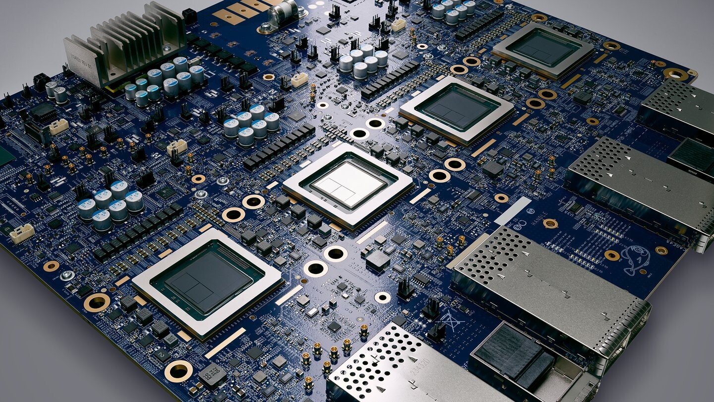
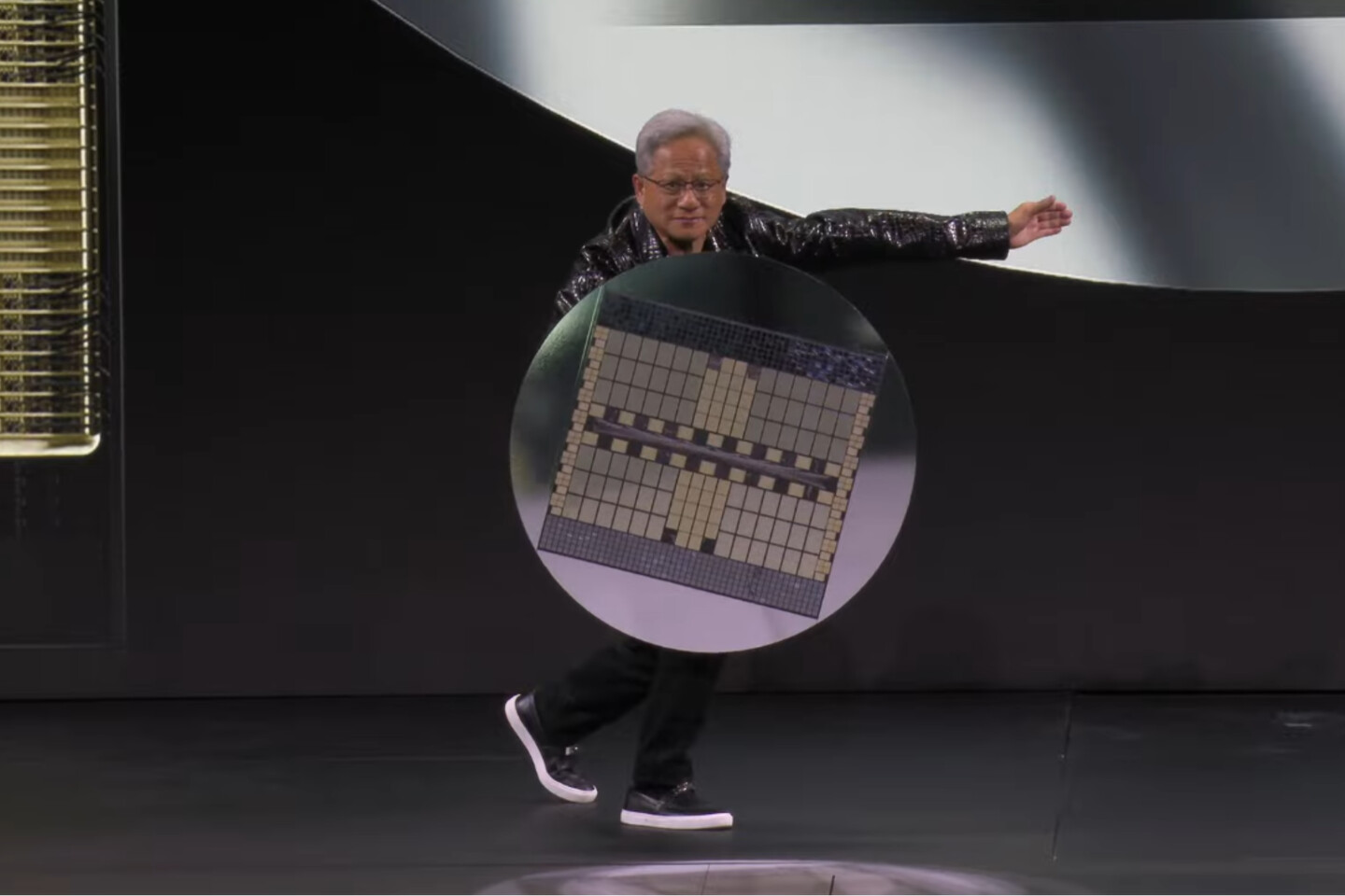
NVIDIA to Consume 77% of Silicon Wafers Dedicated to AI Accelerators in 2025
Investment bank Morgan Stanley has estimated that an astonishing 77% of all globally produced silicon wafers dedicated to AI accelerators will be consumed by none other than NVIDIA. Often, investment research by large investment banks like Morgan Stanley includes information from the semiconductor supply chain, which is constantly expanding to meet NVIDIA's demands. When looking at wafer volume for AI accelerators, it is estimated that in 2024, NVIDIA captured nearly 51% of wafer consumption for its chips, more than half of all demand. With NVIDIA's volume projected to grow to 77%, this represents more than a 50% year-over-year increase, which is incredible for a company of NVIDIA's size. Right now, NVIDIA is phasing out its H100 accelerators in favor of Blackwell 100/200 and the upcoming 300 series of GPUs paired with Grace CPUs.
NVIDIA is accelerating its product deployment timeline and investing a lot in its internal research and development. Morgan Stanley also projects that NVIDIA will invest almost $16 billion in its R&D budget, enough to endure four to five years of development cycles running three design teams sequentially and still delivering new products on an 18-24 month cadence. The scale of this efficiency and development rivals everyone else in the industry. With all this praise, NVIDIA's Q4 revenue report is coming in exactly a week on February 26, so we have to see what its CEO, Jensen Huang, will deliver and show some estimates for the coming months.

NVIDIA is accelerating its product deployment timeline and investing a lot in its internal research and development. Morgan Stanley also projects that NVIDIA will invest almost $16 billion in its R&D budget, enough to endure four to five years of development cycles running three design teams sequentially and still delivering new products on an 18-24 month cadence. The scale of this efficiency and development rivals everyone else in the industry. With all this praise, NVIDIA's Q4 revenue report is coming in exactly a week on February 26, so we have to see what its CEO, Jensen Huang, will deliver and show some estimates for the coming months.

Humane AI Pin To Become $699 Paperweight Post HP Acquisition
The AI Pin - Humane's first, and last product - received an overwhelmingly negative reception at launch, and that's putting it mildly. The device was hindered by poor usability and an extremely laggy operating system that made even the simplest of tasks an absolute chore. The product, unsurprisingly, was criticized by almost every reviewer who touched it, and rumors regarding a potential acquisition of Humane soon began to circulate. Now, HP has seemingly finalized a $116-million acquisition offer for the startup that once raised over $230 million, and valued itself at $1 billion. It appears that HP wants almost all of Humane's assets - with the notable exception of one key product, the AI Pin.
As such, once the calendar reaches the 28th of February, the AI Pin will cease to function. The servers that the AI Pin utilized for communications will be shut down, rendering the AI Pin unable to access customer's cloud data, make phone calls, send AI queries, or text messages. Customers who bought the Pin in the last 90 days will be eligible for a full refund, whereas those who bought the ill-fated gadget before that will soon have an arguably good-looking fashion accessory that will probably still be able to tell them the time. After all, the product's build quality and design was the lone aspect of the AI Pin that received praise. It remains to be seen how HP puts Humane's R&D to use, although considering the AI hype that is engulfing the consumer tech industry, it wouldn't be surprising to see HP leverage Humane's tech to carve out its own niche in the AI-assisted personal computing space. Of course, that is contingent on HP's implementation being better than what Humane pulled off the last time around.

As such, once the calendar reaches the 28th of February, the AI Pin will cease to function. The servers that the AI Pin utilized for communications will be shut down, rendering the AI Pin unable to access customer's cloud data, make phone calls, send AI queries, or text messages. Customers who bought the Pin in the last 90 days will be eligible for a full refund, whereas those who bought the ill-fated gadget before that will soon have an arguably good-looking fashion accessory that will probably still be able to tell them the time. After all, the product's build quality and design was the lone aspect of the AI Pin that received praise. It remains to be seen how HP puts Humane's R&D to use, although considering the AI hype that is engulfing the consumer tech industry, it wouldn't be surprising to see HP leverage Humane's tech to carve out its own niche in the AI-assisted personal computing space. Of course, that is contingent on HP's implementation being better than what Humane pulled off the last time around.


3M Joins Consortium to Accelerate Semiconductor Technology in the US
3M is expanding its commitment to the semiconductor industry by joining the US-JOINT Consortium, a strategic partnership of 12 leading semiconductor suppliers. The consortium drives research and development in next-generation semiconductor advanced packaging and back-end processing technologies anchored by a new cutting-edge facility in Silicon Valley.
"As the demands of AI and other high performance computing technologies increase, suppliers must work together to provide comprehensive solutions to tough challenges on increasingly shorter timelines." said Steven Vander Louw, 3M's president of display and electronics product platforms. "The companies in the US-JOINT Consortium represent US and Japanese innovation leaders in a range of advanced packaging technologies. 3M is pleased to join the consortium in order to bring our decades of materials science expertise, across more than 50 technology platforms, to help address these challenges."
"As the demands of AI and other high performance computing technologies increase, suppliers must work together to provide comprehensive solutions to tough challenges on increasingly shorter timelines." said Steven Vander Louw, 3M's president of display and electronics product platforms. "The companies in the US-JOINT Consortium represent US and Japanese innovation leaders in a range of advanced packaging technologies. 3M is pleased to join the consortium in order to bring our decades of materials science expertise, across more than 50 technology platforms, to help address these challenges."


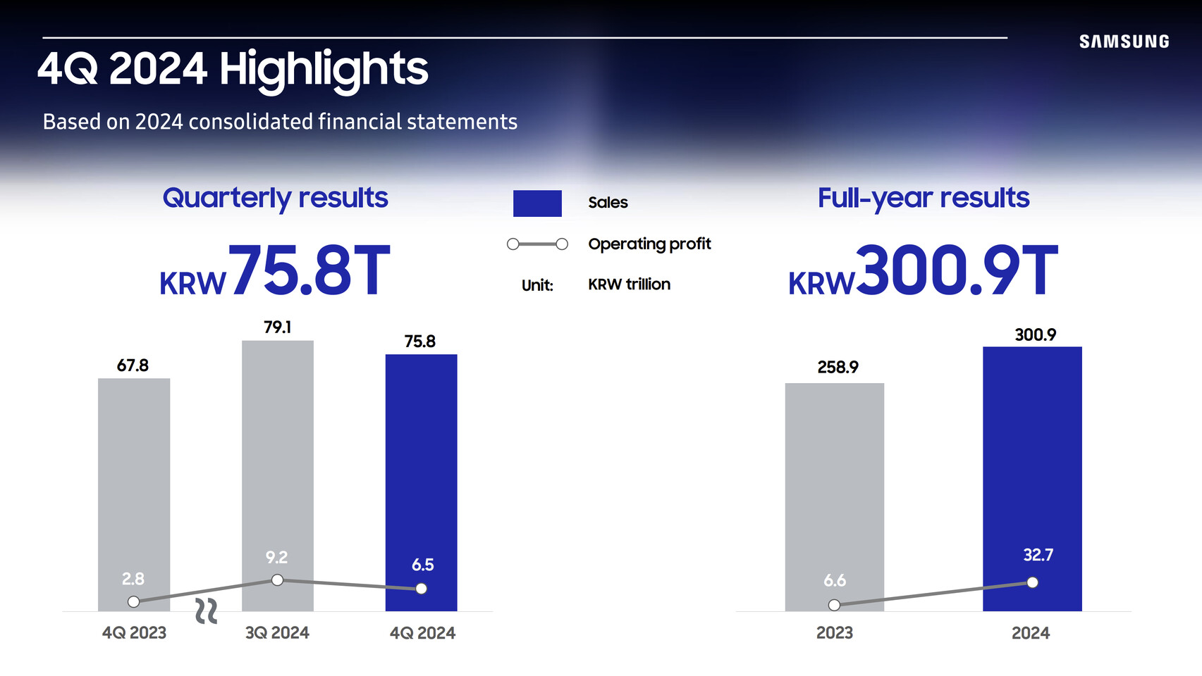
Samsung Electronics Announces Fourth Quarter and FY 2024 Results
Samsung Electronics today reported financial results for the fourth quarter and the fiscal year 2024. The Company posted KRW 75.8 trillion in consolidated revenue and KRW 6.5 trillion in operating profit in the quarter ended December 31, 2024. For the full year, it reported KRW 300.9 trillion in annual revenue and KRW 32.7 trillion in operating profit.
Although fourth quarter revenue and operating profit decreased on a quarter-on-quarter (QoQ) basis, annual revenue reached the second-highest on record, surpassed only in 2022. Meanwhile, operating profit was down KRW 2.7 trillion QoQ, due to soft market conditions especially for IT products, and an increase in expenditures including R&D. In the first quarter of 2025, while overall earnings improvement may be limited due to weakness in the semiconductors business, the Company aims to pursue growth through increased sales of smartphones with differentiated AI experiences, as well as premium products in the Device eXperience (DX) Division.


Although fourth quarter revenue and operating profit decreased on a quarter-on-quarter (QoQ) basis, annual revenue reached the second-highest on record, surpassed only in 2022. Meanwhile, operating profit was down KRW 2.7 trillion QoQ, due to soft market conditions especially for IT products, and an increase in expenditures including R&D. In the first quarter of 2025, while overall earnings improvement may be limited due to weakness in the semiconductors business, the Company aims to pursue growth through increased sales of smartphones with differentiated AI experiences, as well as premium products in the Device eXperience (DX) Division.


U.S. Department of Commerce Announces $1.4 Billion to Support U.S. Semiconductor Advanced Packaging
Today, the U.S. Department of Commerce has announced that CHIPS National Advanced Packaging Manufacturing Program (NAPMP) has finalized $1.4 billion in award funding to bolster U.S. leadership in advanced packaging and enable new technologies to be validated and transitioned at scale to U.S. manufacturing. These awards will help establish a self-sustaining, high-volume, domestic, advanced packaging industry where advanced node chips are both manufactured and packaged in the United States.
These awards include:
These awards include:
- A total of $300 million under the CHIPS NAPMP's first Notice of Funding Opportunity (NOFO) for advanced substrates and material research to Absolics Inc., Applied Materials Inc., and Arizona State University. This follows the previously announced intent to enter negotiations on November 21, 2024
- $1.1 billion to Natcast to operate the advanced packaging capabilities of the CHIPS for America NSTC Prototyping and NAPMP Advanced Packaging Piloting Facility (PPF). This follows the previously announced CHIPS R&D Facilities Model on July 12, 2024, and planned site selection for the PPF on January 6, 2025

NVIDIA AI Expected to Transform $10 Trillion Healthcare & Life Sciences Industry
At yesterday's J.P. Morgan Healthcare Conference NVIDIA announced new partnerships to transform the $10 trillion healthcare and life sciences industry by accelerating drug discovery, enhancing genomic research and pioneering advanced healthcare services with agentic and generative AI. The convergence of AI, accelerated computing and biological data is turning healthcare into the largest technology industry. Healthcare leaders IQVIA, Illumina and Mayo Clinic, as well as Arc Institute, are using the latest NVIDIA technologies to develop solutions that will help advance human health.
These solutions include AI agents that can speed clinical trials by reducing administrative burden, AI models that learn from biology instruments to advance drug discovery and digital pathology, and physical AI robots for surgery, patient monitoring and operations. AI agents, AI instruments and AI robots will help address the $3 trillion of operations dedicated to supporting industry growth and create an AI factory opportunity in the hundreds of billions of dollars.


These solutions include AI agents that can speed clinical trials by reducing administrative burden, AI models that learn from biology instruments to advance drug discovery and digital pathology, and physical AI robots for surgery, patient monitoring and operations. AI agents, AI instruments and AI robots will help address the $3 trillion of operations dedicated to supporting industry growth and create an AI factory opportunity in the hundreds of billions of dollars.


Quobly Announces Key Milestone for Fault-tolerant Quantum Computing
Quobly, a leading French quantum computing startup, has reported that FD-SOI technology can serve as a scalable platform for commercial quantum computing, leveraging traditional semiconductor manufacturing fabs and CEA-Leti's R&D pilot line.
The semiconductor industry has played a pivotal role in enabling classical computers to scale at cost; it has the same transformative potential for quantum computers, making them commercially scalable and cost competitive. Silicon spin qubits are excellent for achieving fault-tolerant, large-scale quantum computing, registering clock speeds in the µsec range, fidelity above 99% for one and two-qubit gate operations and incomparably small unit cell sizes (in the hundredths of 100 nm²).
The semiconductor industry has played a pivotal role in enabling classical computers to scale at cost; it has the same transformative potential for quantum computers, making them commercially scalable and cost competitive. Silicon spin qubits are excellent for achieving fault-tolerant, large-scale quantum computing, registering clock speeds in the µsec range, fidelity above 99% for one and two-qubit gate operations and incomparably small unit cell sizes (in the hundredths of 100 nm²).


Lenovo Group Announces Second Quarter Financial Results 2024/25
Lenovo Group Limited (HKSE: 992) (ADR: LNVGY), together with its subsidiaries ('the Group'), today announced Q2 results for fiscal year 2024/25, reporting significant increases and growth in net income, year-on-year revenue growth for the 4th consecutive quarter, and strong double-digit year-on-year revenue increases from all its business groups. Group revenue increased 24% year-on-year to US$17.9 billion. Net income was up 48% year-on-year to US$404 million on a non-Hong Kong Financial Reporting Standards (non-HKFRS)[1] basis, and non-PC revenue mix was up five points year-to-year to 46%. The Group's results reflect its clear strategy, operational excellence, investment in R&D, innovations in hybrid AI, and global footprint.
The Group's hybrid AI strategy and years of continuous investment in R&D and innovations are paying off, with its first phase of AI PCs, launched in China in May 2024, already reaching double digit share of its total notebook shipments in the China market. Recent launches of AI PCs for the global market with Lenovo AI Now have also been received positively. For enterprise AI, the Group is leveraging its full-stack hybrid infrastructure as well as Lenovo Hybrid AI Advantage to capture growth opportunities. This relentless focus on AI innovation as well as investment in R&D (up 10% year-on-year to US$548 million) is firmly establishing the Group's market differentiation and industry leadership.


The Group's hybrid AI strategy and years of continuous investment in R&D and innovations are paying off, with its first phase of AI PCs, launched in China in May 2024, already reaching double digit share of its total notebook shipments in the China market. Recent launches of AI PCs for the global market with Lenovo AI Now have also been received positively. For enterprise AI, the Group is leveraging its full-stack hybrid infrastructure as well as Lenovo Hybrid AI Advantage to capture growth opportunities. This relentless focus on AI innovation as well as investment in R&D (up 10% year-on-year to US$548 million) is firmly establishing the Group's market differentiation and industry leadership.


LG Display Succeeds in Developing World's First Stretchable Display that Expands by 50 Percent
LG Display, the world's leading innovator of display technologies, announced today its unveiling of the world's first Stretchable display capable of expanding up to 50%, the highest rate of elongation in the industry. At LG Science Park in Seoul on Nov. 8, the company demonstrated the panel at a meeting of more than 100 South Korean industry, academia, and research stakeholders involved in a Stretchable display national project.
Stretchable displays are seen as the ultimate free-form screen technology because they can be freely transformed into any shape, including by stretching, folding, and twisting.

Stretchable displays are seen as the ultimate free-form screen technology because they can be freely transformed into any shape, including by stretching, folding, and twisting.


Apr 16th, 2025 09:18 EDT
change timezone
Latest GPU Drivers
New Forum Posts
- Last game you purchased? (772)
- Help me identify Chip of this DDR4 RAM (20)
- 5070ti overclock...what are your settings? (5)
- Windows 11 fresh install to do list (23)
- How to relubricate a fan and/or service a troublesome/noisy fan. (229)
- GPU Memory Temprature is always high (16)
- Help For XFX RX 590 GME Chinese - Vbios (4)
- PCGH: "hidden site" to see total money spend on steam (3)
- Share your AIDA 64 cache and memory benchmark here (3053)
- NVFlash for RTX 50 Series (Blackwell) (0)
Popular Reviews
- G.SKILL Trident Z5 NEO RGB DDR5-6000 32 GB CL26 Review - AMD EXPO
- ASUS GeForce RTX 5080 TUF OC Review
- DAREU A950 Wing Review
- The Last Of Us Part 2 Performance Benchmark Review - 30 GPUs Compared
- Sapphire Radeon RX 9070 XT Pulse Review
- Sapphire Radeon RX 9070 XT Nitro+ Review - Beating NVIDIA
- Upcoming Hardware Launches 2025 (Updated Apr 2025)
- Thermaltake TR100 Review
- Zotac GeForce RTX 5070 Ti Amp Extreme Review
- TerraMaster F8 SSD Plus Review - Compact and quiet
Controversial News Posts
- NVIDIA GeForce RTX 5060 Ti 16 GB SKU Likely Launching at $499, According to Supply Chain Leak (182)
- NVIDIA Sends MSRP Numbers to Partners: GeForce RTX 5060 Ti 8 GB at $379, RTX 5060 Ti 16 GB at $429 (124)
- Nintendo Confirms That Switch 2 Joy-Cons Will Not Utilize Hall Effect Stick Technology (105)
- Over 200,000 Sold Radeon RX 9070 and RX 9070 XT GPUs? AMD Says No Number was Given (100)
- Nintendo Switch 2 Launches June 5 at $449.99 with New Hardware and Games (99)
- Sony Increases the PS5 Pricing in EMEA and ANZ by Around 25 Percent (85)
- NVIDIA PhysX and Flow Made Fully Open-Source (77)
- NVIDIA Pushes GeForce RTX 5060 Ti Launch to Mid-April, RTX 5060 to May (77)