News Posts matching #SoIC

Return to Keyword Browsing

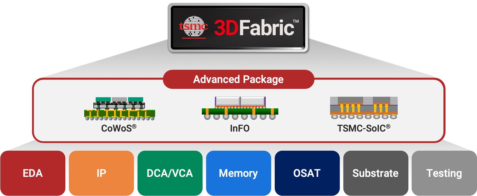
GUC Launches First 32 Gbps per Lane UCIe Silicon Using TSMC 3nm and CoWoS Technology

Global Unichip Corp. (GUC), the Advanced ASIC Leader, today announced the successful launch of industry's first Universal Chiplet Interconnect Express (UCIe) PHY silicon, achieving a data rate of 32 Gbps per lane, the highest speed defined in the UCIe specification. The 32G UCIe IP, supporting UCIe 2.0, delivers an impressive bandwidth density of 10 Tbps per 1 mm of die edge (5 Tbps/mm full-duplex). This milestone was achieved using TSMC's advanced N3P process and CoWoS packaging technologies, targeting AI, high-performance computing (HPC), xPU, and networking applications.

In this test chip, several dies with North-South and East-West IP orientations are interconnected through CoWoS interposer. The silicon measurements show robust 32 Gbps operation with wide horizontal and vertical eye openings. GUC is working aggressively on the full-corner qualification, and the complete silicon report is expected to be available in the coming quarter.

TSMC Showcases New Technology Developments at 2023 Technology Symposium

TSMC today showcased its latest technology developments at its 2023 North America Technology Symposium, including progress in 2 nm technology and new members of its industry-leading 3 nm technology family, offering a range of processes tuned to meet diverse customer demands. These include N3P, an enhanced 3 nm process for better power, performance and density, N3X, a process tailored for high performance computing (HPC) applications, and N3AE, enabling early start of automotive applications on the most advanced silicon technology.

With more than 1,600 customers and partners registered to attend, the North America Technology Symposium in Santa Clara, California is the first of the TSMC's Technology Symposiums around the world in the coming months. The North America symposium also features an Innovation Zone spotlighting the exciting technologies of 18 emerging start-up customers.

TSMC Launches OIP 3DFabric Alliance to Shape the Future of Semiconductor and System Innovations

TSMC today announced the Open Innovation Platform (OIP) 3DFabric Alliance at the 2022 Open Innovation Platform Ecosystem Forum. The new TSMC 3DFabric Alliance is TSMC's sixth OIP Alliance and the first of its kind in the semiconductor industry that joins forces with partners to accelerate 3D IC ecosystem innovation and readiness, with a full spectrum of best-in-class solutions and services for semiconductor design, memory modules, substrate technology, testing, manufacturing, and packaging. This alliance will help customers achieve speedy implementation of silicon and system-level innovations and enable next-generation HPC and mobile applications using TSMC's 3DFabric technologies, a comprehensive family of 3D silicon stacking and advanced packaging technologies.

"3D silicon stacking and advanced packaging technologies open the door to a new era of chip-level and system-level innovation, and also require extensive ecosystem collaboration to help designers navigate the best path through the myriad options and approaches available to them," said Dr. L.C. Lu, TSMC fellow and vice president of design and technology platform. "Through the collective leadership of TSMC and our ecosystem partners, our 3DFabric Alliance offers customers an easy and flexible way to unlocking the power of 3D IC in their designs, and we can't wait to see the innovations they can create with our 3DFabric technologies."

AMD to Implement TSMC SoIC Tech With Upcoming HPC Chips

AMD will debut TSMC's ambitious System-on-Integrated-Chips (SoIC) technology with its upcoming HPC chips, according to a DigiTimes report. A step toward rivaling Intel's Foveros 3-D chip stacking technology, SoIC will enable AMD to stack logic, memory, and I/O as separate chips within a single package. The article references a next-generation "HPC" chip, although it didn't delve into what this could be. Logically, AMD would want to integrate its EPYC and MI accelerator lines into a single package that can be used in HPCs. Such a product would combine its Zen-series x86-64 serial processing, with CDNA-series scalar processing, expertise in memory, leveraging large on-die victim-caches, and high-bandwidth memory (HBM); along with next-gen I/O.
Return to Keyword Browsing
May 6th, 2025 00:36 EDT change timezone

New Forum Posts

Popular Reviews

Controversial News Posts