Kioxia Plans for Wafer-Level SSD
Wafer-scale design is getting popular it seems. Starting from the wafer-scale engine presented by Cerebras last year, which caused quite the shakeup in the industry, it seems that this design approach might be more useful than anyone thought. During VLSI Symposium 2020, Shigeo Oshima, Chief Engineer at Kioxia, had a presentation about new developments in SSD designs and implementations. What was one of the highlights of the presentation was the information that Kioxia is working on, was a technology Kioxia is referring to as wafer-level SSD.
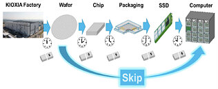
The NAND chips used in SSDs would no longer be cut from the wafer and packaged separately. Instead, the wafer itself would represent the SSD. This is a similar approach Cerebras used with its wafer-scale engine AI processor. What would be gains of this approach compared to traditional methods of cutting up NAND chips and packaging them separately you might wonder? Well, for starters you wouldn't need to cut the wafer, package individual memory chips, and build the SSD out of them. Those steps could be skipped and there would be some cost savings present. And imagine if you decide to do wafer stacking. You could build super scaling SSDs with immense performance capable of millions of IOPS. However, for now, this is only a concept and it is just in early development. There is no possibility to find it in a final product anytime soon.
The NAND chips used in SSDs would no longer be cut from the wafer and packaged separately. Instead, the wafer itself would represent the SSD. This is a similar approach Cerebras used with its wafer-scale engine AI processor. What would be gains of this approach compared to traditional methods of cutting up NAND chips and packaging them separately you might wonder? Well, for starters you wouldn't need to cut the wafer, package individual memory chips, and build the SSD out of them. Those steps could be skipped and there would be some cost savings present. And imagine if you decide to do wafer stacking. You could build super scaling SSDs with immense performance capable of millions of IOPS. However, for now, this is only a concept and it is just in early development. There is no possibility to find it in a final product anytime soon.
