News Posts matching #next-gen

Return to Keyword Browsing

Sony Reportedly Prepping "PlayStation 6 Portable" with "<40 CU" Chipset Design

Sony and Microsoft seem to be involved in the development of handheld gaming consoles, but insiders reckon that respective next-generation offerings will not directly compete with each other. Xbox and ASUS have signalled some sort of collaborative ROG Alloy-esque device; potentially releasing later on in 2025. Whispers of a futuristic PlayStation portable model's chipset design emerged mid-way through March; courtesy of Kepler_L2. The notorious leaker has recent history of reporting inside track knowledge of AMD CPU and GPU architectures/technologies. They alleged that Sony and Team Red's collaborative PS6 APU design project had reached a finalized stage of development, possibly around late 2024/early 2025. Returning to March/April events; Kepler_L2 theorized that a "PS6 Portable" would not be capable of surpassing PlayStation 5 (home console) level performance upon launch in 2028.

The mysterious handheld is said to be powered by a "15 W SoC" manufactured on a non-specific 3 nm node process. Elaborating further, they posit that PlayStation's rumored handheld is capable of running PS5 generation games—bandwidth and power restrictions could reduce resolution and frame rates below that of Sony's current-gen system. Kepler_L2 pictures "PS6 Portable" gaming performance being somewhere in-between Xbox Series S and PlayStation 5 (non-Pro). According to rumors, the handheld's chipset is not related or derived from the PS6 home console's internal setup. Kepler_L2 envisioned a mobile SoC with fewer than 40 compute units (CUs)—several media outlets have added their interpretation of this data point; with a sub-36 count. PlayStation 5's GPU aspect consists of 36 CUs, while the Xbox Series S graphics solution makes do with 20 units. Sony's speculated return to portable territories will be welcomed by owners of older handheld models—namely the Vita and PSP. Famously, these portable products struggled to keep up with competing Nintendo devices.

ASUS ROG Crosshair X870E Extreme Motherboard Launching in China, Price Tag: ~$1360

Since teasing its next-gen flagship motherboard design—at CES 2025—the ASUS Republic of Gamers (ROG) team has spent time finalizing an option that is even more extravagant than their hardcore overclocking-oriented Crosshair X870E Apex model. Naturally, the premium sub-brand did not reveal pricing during preview events—instead, premature European e-tail listings suggested a €1200 (~$1350 USD) tag. Tony Wu and colleagues at ASUS China introduced an impressive swath of brand-new products at an official in-person showcase last week, in Changsha.

During proceedings, company representatives introduced their top-flight E-ATX format board with a hefty day one price: 9999 RMB ($1360 USD). The ASUS ROG Crosshair X870E Extreme is expected to launch later this month; likely starting off with the Chinese domestic market. At the time of writing, the manufacturer's various global branches have not disclosed localized details—be it pricing or availability. Last week's presser did not produce any surprises, since plenty of specification details (and promo shots) leaked out late last month. One interesting and very over the top feature is the model's integration of an adjustable full-color 5-inch LCD screen. The primary M.2 storage solution will be cooled by an "innovative" 3D vapor chamber heatsink. Well-heeled customers will be relieved to know that ASUS has outfitted the AAA board design with their revamped Q-Release Slim mechanism.

Apple "Vision Pro 2" Components Reportedly Being Mass Produced in China

Since its summer 2023 launch, Apple's pricey Vision Pro mixed reality headset has not exactly attracted a mainstream audience. Roughly a year later, rumors of a (then) recently canceled successor appeared online—insiders posited that company engineers had pivoted onto the development of a cheaper alternative model. Vision Pro "Version 1.0" arrived with an intimidating $3499 price tag; thus eliminating interest from a wide swath of potential AR/VR headset enthusiast customers. Industry insiders reckon that Apple had "abruptly reduced production" of the current-gen model last October, with further whispers suggesting a complete cessation of manufacturing activities by the end of 2024. Yesterday, an ITHome article cited compelling claims made by supply chain insiders—the initiation of mass production for a speculated second generation "Apple XR/Vision Pro" device.

The online report stated that: "multiple independent sources (have) confirmed that the panels, shells and other key components of the second-generation Apple XR headset are already in production." Very specific leaked information indicates Lens Technology being the exclusive supplier of glass panel pieces, and Changying Precision tasked with the making of the next-gen model's casing. Additionally, several contract circuit manufacturers are supposedly "rushing to complete orders." Secretive figures posit that Apple will release its sequel mixed reality headset later on in 2025. Differing "expert opinions" have not determined whether this incoming set of fancy goggles will be the predicted "cheaper" model, or a proper "M5 SoC-powered" successor.

Insider Report Suggests Start of 1 nm Chip Development at Samsung, Alleged 2029 Mass Production Phase Targeted

Samsung's foundry business seems to be busying itself with the rumored refinement of a 2 nm GAA (SF2) manufacturing node process—for possible mass production by the end of 2025, but company leadership will very likely be considering longer term goals. Mid-way through last month, industry moles posited that the megacorporation's semiconductor branch was questioning the future of a further out 1.4 nm (SF1.4) production line. Officially published roadmaps have this advanced technology rolling out by 2027. Despite present day "turmoil," insiders believe that a new team has been established—tasked with the creation of a so-called "dream semiconductor process." According to a fresh Sedaily news article, this fledgling department has started development of a 1 nm foundry process.

Anonymous sources claim that Samsung executives are keeping a watchful eye on a main competitor—as stated in the latest South Korean report: "there is a realistic gap with Taiwan's TSMC in technologies that are close to mass production, such as the 2 nm process, the company plans to speed up the development of the 1 nm process, a future technology, to create an opportunity for a turnaround." A portion of the alleged "1 nm development chip team" reportedly consists of veteran researchers from prior-gen projects. Semiconductor industry watchdogs theorize that a canceled SF1.4 line could be replaced by an even more advanced process. Sedaily outlined necessary hardware upgrades: "the 1.0 nanometer process requires a new technology concept that breaks the mold of existing designs as well as the introduction of next-generation equipment such as high-NA EUV exposure equipment. The company is targeting mass production after 2029." Samsung's current Advanced Technology Roadmap does not extend beyond 2027—inside sources claim that the decision to roll with 1.0 nm was made at some point last month.

Nintendo Confirms That Switch 2 Joy-Cons Will Not Utilize Hall Effect Stick Technology

Following last week's jam-packed Switch 2 presentation, Nintendo staffers engaged in conversation with media outlets. To the surprise of many, a high level member of the incoming console's design team was quite comfortable with his name-dropping of NVIDIA graphics technologies. Meanwhile, Team Green was tasked with the disclosing of Switch 2's "internal" workings. Attention has turned to the much anticipated-hybrid console's bundled-in detachable Joy-Cons—in the lead up to official unveilings, online debates swirled around potential next-gen controllers being upgraded with Hall Effect joystick modules. Many owners of first-gen Switch systems have expressed frustration regarding faulty Joy-Cons—eventually, Nintendo was coerced into offering free repairs for customers affected by dreaded "stick drift" issues. Unfortunately, it seems that the House of Mario has not opted to outfit its Gen 2.0 Joy-Cons with popular "anti-drift" tech.

As reported by Nintendo Life, Nate Bihldorff—senior vice president of product development and publishing at Nintendo of America—"outright confirmed the exclusion" of Hall Effect. Up until the publication of Nintendo Life's sit down interview, other company representatives have opined that Switch 2's default control system features very "durable feeling" sticks. When asked about the reason behind "new-gen modules (feeling) so different to the original Switch's analog stick," Bihldorff responded with: "well, the Joy-Con 2's controllers have been designed from the ground up. They're not Hall Effect sticks, but they feel really good. Did you experience both the Joy-Con and the Pro Controller?" The interviewer confirmed that they had prior experience with both new models. In response, Bihldorff continued: "so, I like both, but that Pro Controller, for some reason the first time I grabbed it, I was like, 'this feels like a GameCube controller.' I was a GameCube guy. Something about it felt so familiar, but the stick on that especially. I tried to spend a lot of time making sure that it was quiet. I don't know if you tried really whacking the stick around, but it really is (quiet)...(The Switch 2 Pro Controller) is one of the quietest controllers I've ever played." Nintendo will likely not discuss the "ins and outs" of its proprietary stick design, but inevitable independent teardowns of commercial hardware could verify the provenance of underlying mechanisms. Nowadays, hardcore game controller snobs prefer third-party solutions that sport Tunneling Magnetoresistance (TMR) joysticks.

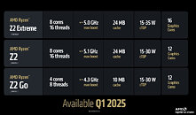
Two Unannounced AMD Ryzen Z2 APU Models Leaked, Flagship Could be "AI Z2 Extreme"

Three months ago, AMD unveiled its Ryzen Z2 APU series at CES 2025—purpose made for deployment in next-gen handheld gaming PCs. The officially announced flagship—Ryzen Z2 Extreme "Strix Point," utilizing Zen 5 and RDNA 3.5 technologies—was previously alluded to by leakers in late 2024; albeit with some curious claims regarding an "odd 3+5 core configuration." Last week, Hoang Anh Phu (@AnhPhuH) presented an alleged expanded lineup of Ryzen Z2 processors—headlined by a mysterious "Ryzen AI Z2 Extreme" SKU.

PC hardware watchdogs believe that this speculative variant will eventually arrive with an enabled XDNA 2 NPU (a first for the series); likely readied to take on Intel's Core Ultra 200V "Lunar Lake" processor family. MSI's Core Ultra 7 258V-powered Claw 8 AI+ and Claw 7 AI+ handhelds launched not too long ago, boasting all sorts of Microsoft Copilot+ capabilities. Mid-way through March, an Xbox executive introduced "Copilot for Gaming." Team Red and manufacturing partners are likely jumping onto this "AI gaming" bandwagon with the aforementioned "AI Ryzen Z2 Extreme" chip, as well as Phu's fanciful "Ryzen Z2 A" model. The latter could be a spin-off of AMD's vanilla Ryzen Z2 "Hawk Point" design, with a "switched on" XDNA NPU.

China Develops HDMI Alternative: 192 Gbps Speeds and 480 W Power Delivery

A consortium of over 50 Chinese companies, including names like Huawei, Hisense, and TCL, has unveiled a domestic alternative to HDMI that offers up to 192 Gbps bandwidth and 480 W of power delivery. This new standard, the General Purpose Media Interface (GPMI), supports next-generation multimedia devices, meeting the growing demands of 8K resolution, higher refresh rates, and simplified connectivity. There are two variants available: a smaller Type-C model providing 96 Gbps and 240 W and a larger Type-B model delivering the full 192 Gbps and 480 W. Developed as a third-generation audio and video interface, GPMI addresses the limitations of older standards such as DVI and VGA while vastly outperforming HDMI 2.1's 48 Gbps and DisplayPort 2.1's 80 Gbps in data throughput. Its design enables bidirectional communication, seamlessly transmitting video, audio, data, and power over a single cable.

The standard's architecture includes a primary data link that can be split into various configurations—such as 6+2 or 1+7 channels—to adapt to different usage scenarios. In addition to its high-bandwidth data channels, GPMI features auxiliary links for device management, cable information, and a limited USB 2.0 connection. The Type-C variant, which has received approval from the USB Association, ensures compatibility with the USB-C ecosystem, helping with the integration for smart TVs and other connected devices. Primarily developed for the domestic market, GPMI also aims to reduce China's dependence on Western-controlled standards and licensing regimes.

Tokyo Electron & IBM Renew Collaboration for Advanced Semiconductor Technology

This week, IBM and Tokyo Electron (TEL) announced an extension of their agreement for the joint research and development of advanced semiconductor technologies. The new 5-year agreement will focus on the continued advancement of technology for next-generation semiconductor nodes and architectures to power the age of generative AI. This agreement builds on a more than two-decade partnership between IBM and TEL for joint research and development. Previously, the two companies have achieved several breakthroughs, including the development of a new laser debonding process for producing 300 mm silicon chip wafers for 3D chip stacking technology.

Now, bringing together IBM's expertise in semiconductor process integration and TEL's leading-edge equipment, they will explore technology for smaller nodes and chiplet architectures to achieve the performance and energy efficiency requirements for the future of generative AI. "The work IBM and TEL have done together over the last 20 years has helped to push the semiconductor technology innovation to provide many generations of chip performance and energy efficiency to the semiconductor industry," said Mukesh Khare, GM of IBM Semiconductors and VP of Hybrid Cloud, IBM. "We are thrilled to be continuing our work together at this critical time to accelerate chip innovations that can fuel the era of generative AI."

Samsung's "All-Solid State" Battery Tech Reportedly Coming to Next-Gen Wearables, No Mention of Deployment in Smartphones

According to a fresh Money Today SK news article, Samsung is expected to launch a next-generation Galaxy Ring model later this year—this tiny wearable device is touted to operate with a "dream battery" design. The South Korean giant's Electro-Mechanics division is reportedly tasked with the challenging development of "all-solid-state" batteries for all manner of ultraportable products. Yesterday's report suggests that Samsung's upcoming Galaxy Ring sequel—apparently scheduled for launch within Q4'25—will be driven by the Electro-Mechanics team's pioneering effort. The production of all-solid-state battery units is an expensive endeavor, so industry watchdogs have predicted tough retail conditions for the forthcoming "Galaxy Ring 2" rollout—the original unit was not exactly a "hot property" in terms of sales figures.

Money Today's inside sources reckon that the Electro-Mechanics branch will—eventually—fit all-solid-state battery designs inside new-gen earphones (aka Galaxy Buds) by Q4 2026, and very futuristic smartwatches by the end of 2027. Given cost considerations, larger all-solid-state solutions—potentially for usage in smartphones—are not in the pipeline. Around early February of this year, the development of Samsung's (inevitable) "Galaxy S26" mobile series was linked to alleged 6000+ mAh silicon-carbon battery units. The South Korean's smartphone engineering team is reportedly trying to play catch up with more advanced solutions, as devised by competitors in China. The status of Samsung's proprietary silicon-carbon prototype is the subject of much online debate, but certain insiders believe that employees are still working hard on the perfection of an ideal "battery formula."

Apple Reportedly Eyeing Late 2025 Launch of M5 MacBook Pro Series, M5 MacBook Air Tipped for 2026

Mark Gurman—Bloomberg's resident soothsayer of Apple inside track info—has disclosed predictive outlooks for next-generation M5 chip-based MacBooks. Early last month, we experienced the launch of the Northern Californian company's M4 MacBook Air series—starting at $999; also available in a refreshing metallic blue finish. The latest iteration of Apple's signature "extra slim" notebook family arrived with decent performance figures. As per usual, press and community attention has turned to a potential successor. Gurman's (March 30) Power On newsletter posited that engineers are already working on M5-powered super slim sequels—he believes that these offerings will arrive early next year, potentially reusing the current generation's 15-inch and 13-inch fanless chassis designs.

In a mid-February predictive report, Gurman theorized that Apple was planning a major overhaul of the MacBook Pro design. A radical reimagining of the long-running notebook series—that reportedly utilizes M6 chipsets and OLED panels—is a distant prospect; perhaps later on in 2026. The Cupertino-headquartered megacorp is expected to stick with its traditional release cadence, so 2025's "M5" refresh of MacBook Pro models could trickle out by October. Insiders believe that Apple will reuse existing MacBook Pro shells—the last major redesign occurred back in 2021. According to early February reportage, mass production of the much-rumored M5 chip started at some point earlier in the year. Industry moles posit that a 3 nm (N3P) node process was on the order books, chez TSMC foundries.

SMIC Reportedly On Track to Finalize 5 nm Process in 2025, Projected to Cost 40-50% More Than TSMC Equivalent

According to a report produced by semiconductor industry analysts at Kiwoom Securities—a South Korean financial services firm—Semiconductor Manufacturing International Corporation (SMIC) is expected to complete the development of a 5 nm process at some point in 2025. Jukanlosreve summarized this projection in a recent social media post. SMIC is often considered to be China's flagship foundry business; the partially state-owned organization seems to heavily involved in the production of (rumored) next-gen Huawei Ascend 910 AI accelerators. SMIC foundry employees have reportedly struggled to break beyond a 7 nm manufacturing barrier, due to lack of readily accessible cutting-edge EUV equipment. As covered on TechPowerUp last month, leading lights within China's semiconductor industry are (allegedly) developing lithography solutions for cutting-edge 5 nm and 3 nm wafer production.

Huawei is reportedly evaluating an in-house developed laser-induced discharge plasma (LDP)-based machine, but finalized equipment will not be ready until 2026—at least for mass production purposes. Jukanlosreve's short interpretation of Kiwoom's report reads as follows: (SMIC) achieved mass production of the 7 nm (N+2) process without EUV and completed the development of the 5 nm process to support the mass production of the Huawei Ascend 910C. The cost of SMIC's 5 nm process is 40-50% higher than TSMC's, and its yield is roughly one-third." The nation's foundries are reliant on older ASML equipment, thus are unable to produce products that can compete with the advanced (volume and quality) output of "global" TSMC and Samsung chip manufacturing facilities. The fresh unveiling of SiCarrier's Color Mountain series has signalled a promising new era for China's foundry industry.

"GFX1153" Target Spotted in AMDGPU Library Amendment, RDNA 3.5 Again Linked to "Medusa Point" APU

At the tail end of 2024, AMD technical staffers added the "GFX1153" target to their first-party GPU supported chip list. Almost three months later, PC hardware news outlets and online enthusiasts have just picked up on this development. "GFX1150" family IPs were previously linked to Team Red's RDNA 3.5 architecture. This graphics technology debuted with the launch of Ryzen AI "Strix Halo," "Strix Point" and "Krackan Point" mobile processors. Recent leaks have suggested that Team Red is satisfied with the performance of RDNA 3.5-based Radeon iGPUs; warranting a rumored repeat rollout with next-gen "Medusa Point" APU designs.

Both "Medusa Point" and "Gorgon Point" mobile CPU families are expected to launch next year, with leaks pointing to the utilization of "Zen 6" and "Zen 5" processor cores (respectively) and RDNA 3.5 graphics architecture. RDNA 4 seems to be a strictly desktop-oriented generation. AMD could be reserving the "further out" UDNA tech for truly next-generation integrated graphics solutions. In the interim, Team Red's "GFX1153" IP will likely serve as "Medusa Point's" onboard GPU, according to the latest logical theories. Last year, the "GFX1152" target was associated with Ryzen AI 7 300-series "Krackan Point" APUs.

NVMe Hard Drives: Seagate's Answer to Growing AI Storage Demands

Seagate is advancing in NVMe technology for large-capacity hard drives as the growing storage needs in AI systems and apps continue to rise. Old and current storage setups struggle to handle the huge datasets needed for machine learning, which now reach petabyte and even exabyte sizes. Today's storage options have many drawbacks for AI tasks. SSD-based systems offer the needed speed however it is not cost-effective for storing large AI training data. SAS/SATA hard drives are cheaper however, the interfaces rely on proprietary silicon, host bus adapters (HBAs), and controller architectures that struggle with the high-throughput, low-latency needs of AI's high data flow.

Seagate's "new idea" is to use NVMe technology in large-capacity hard drives. This creates a solution that keeps hard drives cost-effective and dense while boosting performance for AI apps. NVMe hard drives will not need HBAs, protocol bridges, and additional SAS infrastructure, allowing seamless scalability by integrating high-density hard drive storage with high-speed SSD caching in a unified NVMe architecture.

Leak Indicates Nintendo Switch 2 Utilizing 120 Hz LCD Screen with VRR & HD Capabilities

As expected, Nintendo has kept quiet about the upcoming Switch 2 hybrid console's feature set and internal makeup. The next-gen portable gaming system's debut presentation served as a mostly surface-level teaser. News outlets have relied heavily on leaks for "insider" reportage, going back to the early 2020s—starting off with kopite7kimi's discovery of a mysterious NVIDIA "T239" chipset. As reported last week, Famiboards—a Nintendo-centric online forum—has served as a somewhat reliable source of inside track information. Earlier in the year, one member started to share NDA-busting details about Switch 2's display technology: "I've heard that the screen supports 120 Hz and VRR, which should help a lot in handheld." Weeks later, SecretBoy elaborated on the benefits of this setup: "developers can optimize the handheld profiles of their games with VRR and 40 FPS in mind."

The GamingLeaksAndRumours subreddit views SecretBoy's leaks as being fairly accurate/legitimate: "(they) called out the GPU performance before the clock speeds were leaked; 10 days later back in January (3 TFLOPS docked, 1.4/1.5 TFLOPS handheld)." Earlier today, the tipster's latest musings were compiled into a Reddit summary—another set of quotes reads as follows (in condensed form): "I will reiterate that the screen is 120 Hz with HDR and VRR support. That's what I'm personally most excited for...No idea about the actual quality of the screen, but I think OLED was always going to be too expensive for this feature set, which they needed to get into the first iteration of the hardware so that developers could optimize their games around it (speculation)." Screen technology connoisseurs have expressed much disappointment about Nintendo's alleged selection of an "inferior" panel—many will point out that Valve was inspired by the Switch OLED model (2021); their Steam Deck handheld was famously upgraded/refreshed in 2023 with a fancier screen. Invited guests will get to experience Switch 2's "hugely revelatory" LCD tech at various Nintendo-hosted international preview events in April.

Leak Suggests Recent Arrival of Significant Nintendo Switch 2 Shipments on US Shores

Nintendo seems to readying a speculated mid-2025 launch of the much-anticipated Nintendo Switch 2 hybrid games console, according to industry watchdogs. International preview events are scheduled to happen throughout April, so online theories have settled on potential May or June release windows. Members of Famiboards—a Nintendo discussion forum—have kept tabs on a wide variety of pre-launch information outlets, going back to 2021. Their latest tracking activities—with eyes firmly trained on shipping manifests—have produced compelling evidence of Switch 2 materials turning up on North American shores in the recent past. A Famiboards detective detailed their discoveries: "so, it finally happened. HVBG exported 383,000 units of the completed console set between January 17th and January 22nd. They were all shipped to the US, and all were of the USZ (US/Canada) region code. 41,598 units of the charging grip were also shipped to the US, confirming that HGU0620 is the charging grip with a product code of BEE-A-ESSKA, which matches the Switch 1 charging grip's HAC-A-ESSKA."

Nintendo's mid-January unveiling of Switch 2 served as a refreshing break from the norm; the Japanese gaming giant operates under very secretive conditions. Their early 2025 teaser showcased a device that seemed to recycle its predecessor's feature set, but the CGI trailer implied mouse-like functionality. Patent leaks have provided further insight into the design of Nintendo's next-gen Joy-Con. Last month, Shuntaro Furukawa—the company's president—disclosed that his team was taking "all possible measures" to provide sufficient stock for Switch 2's launch window. This week's insider investigation paints a promising picture, at least for potential North American buyers: "383k is a decent-sized shipment, but I wouldn't be surprised if the numbers increase. HVBG had received 1.2 million units of one-per-system parts like the SoC and screen as of December, and 1.7 million as of January, and we can expect 100% of those to end up in units shipped to the US. One thing we can learn from the shipments is that the console set is not a bundle."

Samsung Reportedly Planning Mass Production of "Exynos 2600" Prototypes in May

Late last month, industry insiders posited that pleasing progress was being made with Samsung's cutting-edge 2 nm Gate-All-Around (GAA) node process. The rumored abandonment of an older 3 nm GAA-based project—in late 2024—has likely sent the South Korean foundry team into overdrive. A speculated Exynos 2500 flagship mobile processor was previously linked to said 3 nm node, but industry watchdogs believe that company engineers are experimenting with a 2 nm GAA manufacturing process. According to the latest insider report—from FN News SK—Samsung Foundry (SF) has assembled a special "task force (TF)." Allegedly, this elite team will be dedicated to getting a newer "Exynos 2600 chip" over the finish line—suggesting an abandonment of the older "2500" design, or a simple renaming.

Samsung's recent launch of Galaxy S25 series smartphones was reportedly viewed as a disappointing compromise—with all models being powered by Qualcomm's "first-of-its-kind customized Snapdragon 8 Elite Mobile Platform," instead of in-house devised chipsets. According to industry moles, one of the SF task force's main goals is a boosting of 2 nm GAA production yields up to "economically viable" levels (roughly 60-70%)—apparently last month's best result was ~30%. Mass production of prototype chipsets is tipped to start by May. Samsung's reported target of "stabilizing their Exynos 2600" SoC design will ensure that "Galaxy S26 series" devices will not become reliant on Qualcomm internals. Additionally, FN News proposes a bigger picture scenario: "the stabilization of 2 nm (SF2/GAA) products, is expected to speed up the acquisition of customers for Samsung Electronics' foundry division, which is thirsty for leading-edge process customers." A forthcoming rival next-gen mobile chip—Snapdragon 8 Elite Gen 2—is supposedly in the pipeline. The smartphone industry inside track reckons that Qualcomm has signed up with TSMC; with a 2 nm manufacturing process in mind.

Physical SIM Support Reportedly in the Balance for Ultra-thin Smartphones w/ Snapdragon 8 Elite Gen 2 SoCs

According to Digital Chat Station—a repeat leaker of unannounced Qualcomm hardware—unnamed Android smartphone manufacturers are considering an eSIM-only operating model for future flagship devices. Starting with the iPhone 14 generation (2022), Apple has continued to deliver gadgets that are not reliant on "slotted-in" physical SIM cards. According to industry insiders, competitors could copy the market leader's homework—Digital Chat Station's latest Weibo blog post discusses the space-saving benefits of eSIM operation; being "conducive to lightweight and integrated design." Forthcoming top-tier slimline Android mobile devices are tipped to utilize Qualcomm's rumored second-generation "Snapdragon 8 Elite Gen 2" (SM8850) chipset.

Digital Chat Station reckons that: "SM8850 series phones at the end of the year are testing eSIM. Whether they can be implemented in China is still a question mark. Let's wait and see the iPhone 17 Air. In order to have an ultra-thin body, this phone directly cancels the physical SIM card slot. Either it will be a special phone for the domestic market, or it will get eSIM." The phasing out of physical SIM cards within the Chinese mobile market could be a tricky prospect for local OEMs, but reports suggest that "traditionally-dimensioned" flagship offerings will continue to support the familiar subscriber identity module standard. Physical SIM card purists often point out that the format still provides superior network support range.

Insiders Cast Doubt on Finalization of Apple M4 Ultra Chip, Cite Production & Cost Challenges

Apple's recent unveiling of refreshed Mac Studio models—in "mismatched" M3 Ultra and M4 Max forms—was greeted with a lukewarm reception from press and public. The absence of an M4 Ultra option has disappointed many folks within the high-end Mac buying populace—rumors of a delayed development of Apple's "Mac Studio M4 Ultra model" emerged online last October. The M3 Ultra processor serves as a somewhat dissatisfying stopgap—prior to last week's official announcement, insiders were still actively questioning the existence of said chip. Last week, Apple representatives reportedly informed Ars Technica and Numerama about their "Ultra" tier not reaching "every chip generation." Follow-up articles have suggested that the M4 Max chip design does not feature an UltraFusion connector; thus cutting off a main path to potential M4 Ultra routes.

Based on previous-gen history, Mac-specialist news sites propose the upcoming M3 Ultra chipset being—in effect—the result of two M3 Max chips joined together via Apple's UltraFusion connection system. Further speculation points to the company's engineering department having to start with a blank canvas; involving a speculative monolithic die design. Noted Apple leaker—Mark Gurman—has disclosed additional theories via his paywalled Bloomberg "Power On" newsletter. As interpreted by MacRumors: "Apple is reluctant to develop an M4 Ultra chip from scratch due to production challenges, costs, and the relatively small sales volume of its desktop computers, like the Mac Studio. So, that seems to rule out the only other way in which Apple could have released an M4 Ultra chip." Several media outlets posit that Apple will skip a generation, and instead focus on getting UltraFusion connections working with next-gen "M5" processors. A refreshed Mac Pro lineup is reportedly on the cards; mid-January reports linked the next-gen workstation series to a very powerful "Hidra" chip design.

MiTAC Computing Showcases Cutting-Edge AI and HPC Servers at Supercomputing Asia 2025

MiTAC Computing Technology Corp., a subsidiary of MiTAC Holdings Corp. and a global leader in server design and manufacturing, will showcase its latest AI and HPC innovations at Supercomputing Asia 2025, taking place from March 11 at Booth #B10. The event highlights MiTAC's commitment to delivering cutting-edge technology with the introduction of the G4520G6 AI server and the TN85-B8261 HPC server—both engineered to meet the growing demands of artificial intelligence, machine learning, and high-performance computing (HPC) applications.

G4520G6 AI Server: Performance, Scalability, and Efficiency Redefined
The G4520G6AI server redefines computing performance with an advanced architecture tailored for intensive workloads. Key features include:
  • Exceptional Compute Power- Supports dual Intel Xeon 6 Processors with TDP up to 350 W, delivering high-performance multicore processing for AI-driven applications.
  • Enhanced Memory Performance- Equipped with 32 DDR5 DIMM slots (16 per CPU) and 8 memory channels, supporting up to 8,192 GB DDR5 RDIMM/3DS RDIMM at 6400 MT/s for superior memory bandwidth.

Intel Panther Lake on Track for H2 2025 Launch, Company Exec Disregards Rumors of 18A Delays

Earlier in the week, online chatter pointed to a possible delay in the production of Panther Lake silicon. Well-known industry analyst—Ming-Chi Kuo—has kept tabs on the inner workings of several big semiconductor players. A previous insider tale revealed NVIDIA's allegedly revised "Blackwell" architecture roadmap. Kuo's latest insight focused on Intel and their 18A node process; rumored setbacks have reportedly pushed the launch of next-gen Panther Lake (PTL) mobile processors into 2026. Team Blue leadership has already reacted to the relatively fresh allegations—earlier in the week, John Pitzer sat down with Morgan Stanley Semiconductor Research's Joe Moore. During their conference fireside chat, Intel's Corporate Vice President of Investor Relations addressed recent internet whispers.

When asked about 18A being developed on schedule, Pitzer responded with: "yes, it is. I mean, I tend to wake up every morning trying to fish through rumors that are coming across on social media about Intel 18A. I want to be very clear. Panther Lake is on track to launch in the second half of this year. That launch date has not changed. We feel really good about the progress that we are making. In fact, if you look at where our yields are on Panther Lake today, they're actually slightly ahead at a similar point in time to Meteor Lake, if you look at the development process for Meteor Lake. I think a couple of weeks ago, there was a technical paper out that actually looked at our SRAM density on Intel 18A that compared well with TSMC's N2. Lots of different metrics you can compare technologies on. I think in general, we think about Intel 18A being an N3 type/N2 sort of comp with the external peers." Panther Lake is set to become the company's first product family that will utilize its own Foundry's 18A node process. Mid-way through February, we heard about the importance of PTL with Intel's portable gaming strategy.

AMD "Medusa Point" Mobile APU Design Linked to RDNA 3.X, Instead of RDNA 4

The "Medusa" or "Medusa Point" codename started to appear online over the past couple of months. These mysterious AMD projects were linked to next-generation "Zen 6" Ryzen desktop and mobile processor families (respectively). Initially, insiders reckoned that Team Red had selected an RDNA 4-based graphics solution for integration their futuristic new-gen laptop APU design. Two days ago, Golden Pig Upgrade weighed in with a different theory—the veteran leaker believes that provisions have regressed on the "Medusa Point" iGPU front.

Previous reports have suggested that the "Medusa Point" processor's iGPU aspect will utilize up to 16 compute units (CU), based on a theorized count of eight workgroup processors (WGPs) from leaked imagery. The latest insider tip points to the utilization of a non-specific "RDNA 3.x" branch, instead of conjectured RDNA 4 graphics technology. Industry watchdogs hold the belief that AMD will be sticking with RDNA 3.5 for a while—as featured on their current-gen "Zen 5" mobile-oriented Strix Point, Strix Halo and Krackan Point chips. As pointed out by Notebookcheck, Team Red leadership disclosed that RDNA 4 is exclusive to discrete card families (for the time being). RDNA 3.5-equipped APUs have—so far—received a warm welcome; AMD engineers could be reserving development resources for a distant future project.

SoftBank, ZutaCore and Foxconn Collaborate on Development of Rack-Integrated Solution

SoftBank Corp., ZutaCore and Hon Hai Technology Group ("Foxconn") today announced they implemented ZutaCore's two-phase DLC (Direct Liquid Cooling) technology in an AI server using NVIDIA accelerated computing, making it the world's first implementation of ZutaCore's two-phase DLC (Direct Liquid Cooling) technology using NVIDIA H200 GPUs. In addition, SoftBank designed and developed a rack-integrated solution that integrates each component of the server, including cooling equipment with two-phase DLC technology, on a rack scale, and conducted an operational demonstration and performance evaluation at its data center in February 2025. The demonstration results indicated the solution passed NVIDIA's temperature test (NVQual), thereby confirming the compatibility, stability and reliability of this rack-integrated solution. The solution also achieved pPUE (partial Power Usage Effectiveness) of 1.03 (actual measured value) per rack for cooling efficiency

With the spread and increased adoption of AI, demand for AI servers and other computing resources is expected to expand significantly, further increasing power consumption at data centers. At the same time, reducing power consumption from the perspective of reducing carbon dioxide (CO2) emissions has become a pressing issue worldwide, requiring data centers to become more efficient, consume less power, and introduce innovative heat removal solutions. Since May 2024, SoftBank has been collaborating with ZutaCore, a global leader in the development and business deployment of two-phase DLC technology, to develop solutions optimized for low power consumption at AI data centers.

AMD Debuted Radeon RX 9070 Series MSRPs in China, 12 Hours Ahead of Global Event

International corporate entities have to deal with global time differences; causing uncountable logistical headaches. As evidenced by local reports; AMD and board partner representatives decided to debut their next-gen Radeon RX 9070 Series in front of a (mostly) Chinese audience. The much earlier than anticipated presentation took place well in advance of the "main event," with Jack Huynh and other Team Red big brass showcasing brand-new products to regional distributors and media outlets. VideoCardz believes that this "surprise" press mini-junket occurred—roughly—twelve hours ahead of the officially scheduled international "special broacast."

Baseline price points—VAT included—of 4999 RMB (~$686 USD) and 4499 RMB (~$617 USD) were announced, for the incoming Radeon RX 9070 XT and RX 9070 models (respectively). We now know that North American MSRPs (excluding tax) are $599 and $549 (respectively). AMD's presentation slides included more shots of their reference designs (MBA), in triple or dual-fan configurations. Earlier in the week, industry watchdogs proposed that the Radeon RX 9070 Series would launch with an all-custom card lineup; with no AMD-built options. Attendees noted several on-stage board partner company reps, including Jack Yu (ASUS China). ASRock, GIGABYTE, PowerColor, VASTARMOR, XFX and Yeston were the other participants; with demonstration hardware in their hands.

Samsung Display's OCF Leadership Takes Center Stage at MWC25

Samsung Display today revealed plans to exhibit its next-generation OLED technology, boasting an impressive maximum brightness of 5,000 nits, at the Mobile World Congress 2025 (MWC25) on March 3.

The ultra-high brightness OLED was developed based on the polarizer-less display, also known as on-cell film (OCF) technology, which Samsung Display was the first to commercialize. This innovation not only enhances outdoor visibility but also reduces power consumption, paving the way for significant design flexibility. OCF technology is being applied to a bar-type smartphone and a rollable laptop, following its success in foldable smartphones, and is being recognized by customers as a high-value display technology.

AMD to Discuss Advancing of AI "From the Enterprise to the Edge" at MWC 2025

GSMA MWC Barcelona, runs from March 3 to 6, 2025 at the Fira Barcelona Gran Via in Barcelona, Spain. AMD is proud to participate in forward-thinking discussions and demos around AI, edge and cloud computing, the long-term revolutionary potential of moonshot technologies like quantum processing, and more. Check out the AMD hospitality suite in Hall 2 (Stand 2M61) and explore our demos and system design wins. Attendees are welcome to stop by informally or schedule a time slot with us.

As modern networks evolve, high-performance computing, energy efficiency, and AI acceleration are becoming just as critical as connectivity itself. AMD is at the forefront of this transformation, delivering solutions that power next-generation cloud, AI, and networking infrastructure. Our demos this year showcase AMD EPYC, AMD Instinct, and AMD Ryzen AI processors, as well as AMD Versal adaptive SoC and Zynq UltraScale+ RFSoC devices.
Return to Keyword Browsing
Apr 17th, 2025 09:48 EDT change timezone

New Forum Posts

Popular Reviews

Controversial News Posts