Apr 16th, 2025 13:03 EDT
change timezone
Latest GPU Drivers
New Forum Posts
- The TPU UK Clubhouse (26127)
- What's your latest tech purchase? (23561)
- Tried installing 576.02 - installer window disappears (1)
- Need advice RAM for Asus Maximus hero z890 + core ultra 7 265k (4)
- i9-14900HX Running Hot — FIVR Undervolting Locked (3)
- How to relubricate a fan and/or service a troublesome/noisy fan. (233)
- 5070 Ti power limit questions (34)
- RX 9000 series GPU Owners Club (332)
- DTS DCH Driver for Realtek HDA [DTS:X APO4 + DTS Interactive] (2143)
- How to modify the laptop BIOS to allow it to recognize larger onboard memory (2)
Popular Reviews
- G.SKILL Trident Z5 NEO RGB DDR5-6000 32 GB CL26 Review - AMD EXPO
- ASUS GeForce RTX 5080 TUF OC Review
- ASUS GeForce RTX 5060 Ti TUF OC 16 GB Review
- DAREU A950 Wing Review
- The Last Of Us Part 2 Performance Benchmark Review - 30 GPUs Compared
- Sapphire Radeon RX 9070 XT Pulse Review
- Sapphire Radeon RX 9070 XT Nitro+ Review - Beating NVIDIA
- Upcoming Hardware Launches 2025 (Updated Apr 2025)
- Zotac GeForce RTX 5070 Ti Amp Extreme Review
- Thermaltake TR100 Review
Controversial News Posts
- NVIDIA GeForce RTX 5060 Ti 16 GB SKU Likely Launching at $499, According to Supply Chain Leak (182)
- NVIDIA Sends MSRP Numbers to Partners: GeForce RTX 5060 Ti 8 GB at $379, RTX 5060 Ti 16 GB at $429 (126)
- Nintendo Confirms That Switch 2 Joy-Cons Will Not Utilize Hall Effect Stick Technology (105)
- Over 200,000 Sold Radeon RX 9070 and RX 9070 XT GPUs? AMD Says No Number was Given (100)
- Nintendo Switch 2 Launches June 5 at $449.99 with New Hardware and Games (99)
- Sony Increases the PS5 Pricing in EMEA and ANZ by Around 25 Percent (85)
- NVIDIA Pushes GeForce RTX 5060 Ti Launch to Mid-April, RTX 5060 to May (77)
- NVIDIA PhysX and Flow Made Fully Open-Source (77)
News Posts matching #substrate
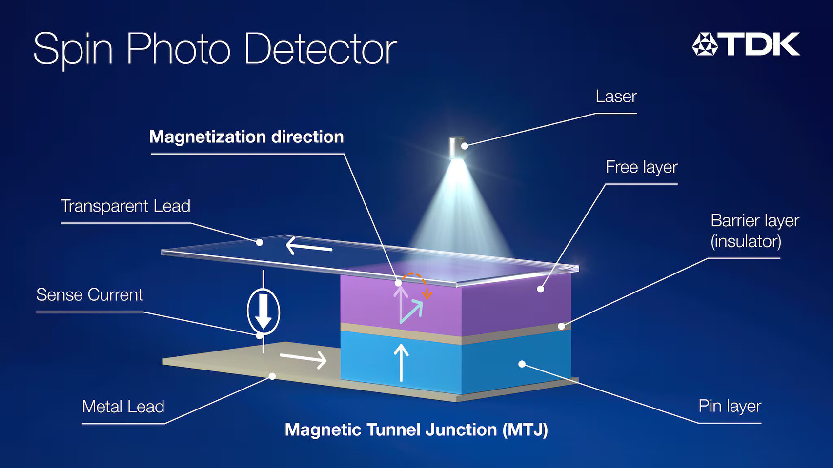
Return to Keyword BrowsingTDK Demonstrates the World's First "Spin Photo Detector" Capable of 10X Data Transmission Speeds
TDK Corporation announces that it has developed the world's first "Spin Photo Detector," a photo-spintronic conversion element combining optical, electronic, and magnetic elements that can respond at an ultra-high speed of 20 picoseconds (20 × 10⁻¹² s) using light with a wavelength of 800 nm - more than 10X faster than conventional semiconductor-based photo detectors. This new device is expected to be a key driver for implementing photoelectric conversion technology that boosts data transmission and data processing speed, particularly in AI applications, while simultaneously reducing power consumption.
Transferring mass amounts of data at higher speeds and with lower power consumption is an inevitable need as AI evolves. To process data and make calculations, data is currently transferred between CPU/GPU chips as well as from and to memory by electrical signals. Therefore, there is an increasing need for optical communication and optical interconnects, which offer high speeds that do not decrease with interconnect distance. Photoelectronic conversion technology is also gaining global interest as a very compact fusion of both optical and electronic elements.
Transferring mass amounts of data at higher speeds and with lower power consumption is an inevitable need as AI evolves. To process data and make calculations, data is currently transferred between CPU/GPU chips as well as from and to memory by electrical signals. Therefore, there is an increasing need for optical communication and optical interconnects, which offer high speeds that do not decrease with interconnect distance. Photoelectronic conversion technology is also gaining global interest as a very compact fusion of both optical and electronic elements.

Open Compute Project Foundation and JEDEC Announce New Chiplet Design Kits
Today, the Open Compute Project Foundation (OCP), the nonprofit organization bringing hyperscale innovations to all, and JEDEC Solid State Technology Association, the global leader in the development of standards for the microelectronics industry, announce the availability of new Chiplet Design Kits for use with today's EDA tools covering Assembly, Substrate, Material and Test developed in collaboration within the OCP Open Chiplet Economy Project. Leveraging the alliance between OCP and JEDEC, these design kits are now part of the Global Worldwide Standard JEDEC JEP30: Part Model Guidelines.
The release of the Assembly, Substrate, Material, and Test Design Kits build on earlier joint efforts between the OCP and JEDEC integrating OCP Chiplet Data Extensible Markup Language (CDXML) specification into JEDEC JEP30: Part Model Guidelines, enabling Chiplet builders to provide electronically a standardized Chiplet part description to their customers, paving the way for automating System-in-Package (SiP) design and build using Chiplets.

The release of the Assembly, Substrate, Material, and Test Design Kits build on earlier joint efforts between the OCP and JEDEC integrating OCP Chiplet Data Extensible Markup Language (CDXML) specification into JEDEC JEP30: Part Model Guidelines, enabling Chiplet builders to provide electronically a standardized Chiplet part description to their customers, paving the way for automating System-in-Package (SiP) design and build using Chiplets.


IBM Develops Co-Packaged Optical Interconnect for Data Center
IBM Research has unveiled a significant advancement in optical interconnect technology for advanced data center communications. The breakthrough centers on a novel co-packaged optics (CPO) system featuring a sophisticated Polymer Optical Waveguide (PWG) design, marking a potential shift from traditional copper-based interconnects. The innovation introduces a Photonic Integrated Circuit (PIC) measuring 8x10mm, mounted on a 17x17mm substrate, capable of converting electrical signals to optical ones and vice versa. The system's waveguide, spanning 12 mm in width, efficiently channels light waves through precisely engineered pathways, with channels converging from 250 to 50 micrometers.
While current copper-based solutions like NVIDIA's NVLink offer impressive 1.8 TB/s bandwidth rates, and Intel's Optical Compute Interconnect achieves 4 TBit/s bidirectional throughput, IBM's technology focuses on scalability and efficiency. The company plans to implement 12 carrier waves initially, with the potential to accommodate up to 32 waves by reducing spacing to 18 micrometers. Furthermore, the design allows for vertical stacking of up to four PWGs, potentially enabling 128 transmission channels. The technology has undergone rigorous JEDEC-standard testing, including 1,000 cycles of thermal stress between -40°C and 125°C, and extended exposure to extreme conditions including 85% humidity at 85°C. The components have also proven reliable during thousand-hour storage tests at various temperature extremes. The bandwidth of the CPO is currently unknown, but we expect it to surpass current solutions.

While current copper-based solutions like NVIDIA's NVLink offer impressive 1.8 TB/s bandwidth rates, and Intel's Optical Compute Interconnect achieves 4 TBit/s bidirectional throughput, IBM's technology focuses on scalability and efficiency. The company plans to implement 12 carrier waves initially, with the potential to accommodate up to 32 waves by reducing spacing to 18 micrometers. Furthermore, the design allows for vertical stacking of up to four PWGs, potentially enabling 128 transmission channels. The technology has undergone rigorous JEDEC-standard testing, including 1,000 cycles of thermal stress between -40°C and 125°C, and extended exposure to extreme conditions including 85% humidity at 85°C. The components have also proven reliable during thousand-hour storage tests at various temperature extremes. The bandwidth of the CPO is currently unknown, but we expect it to surpass current solutions.


Intel Foundry Unveils Technology Advancements at IEDM 2024
Today at the IEEE International Electron Devices Meeting (IEDM) 2024, Intel Foundry unveiled new breakthroughs to help drive the semiconductor industry forward into the next decade and beyond. Intel Foundry showcased new material advancements that help improve interconnections within a chip, resulting in up to 25% capacitance by using subtractive ruthenium. Intel Foundry also was first to report a 100x throughput improvement using a heterogeneous integration solution for advanced packaging to enable ultra-fast chip-to-chip assembly. And to further drive gate-all-around (GAA) scaling, Intel Foundry demonstrated work with silicon RibbonFET CMOS and with gate oxide module for scaled 2D FETs for improved device performance.
"Intel Foundry continues to help define and shape the roadmap for the semiconductor industry. Our latest breakthroughs underscore the company's commitment to delivering cutting-edge technology developed in the U.S., positioning us well to help balance the global supply chain and restore domestic manufacturing and technology leadership with the support of the U.S. CHIPS Act," says Sanjay Natarajan, Intel senior vice president and general manager of Intel Foundry Technology Research.
"Intel Foundry continues to help define and shape the roadmap for the semiconductor industry. Our latest breakthroughs underscore the company's commitment to delivering cutting-edge technology developed in the U.S., positioning us well to help balance the global supply chain and restore domestic manufacturing and technology leadership with the support of the U.S. CHIPS Act," says Sanjay Natarajan, Intel senior vice president and general manager of Intel Foundry Technology Research.

Smartkem and AUO Partner to Develop a New Generation of Rollable, Transparent MicroLED Displays
Smartkem, positioned to power the next generation of displays using its disruptive organic thin-film transistors (OTFTs), has partnered with AUO, the largest display manufacturer in Taiwan, to jointly develop the world's first advanced rollable, transparent microLED display using Smartkem's technology.
"We believe that collaborating with global display industry leader AUO to develop a novel microLED display puts Smartkem's technology on the frontier of microLED display commercialization. Our unique transistor technology is expected to enable display manufacturers to efficiently produce microLED displays, making mass production commercially viable. Smartkem's technology has the potential to take today's microLED TVs from high end market prices of $100,000 down to mass market prices," stated Ian Jenks, Smartkem Chairman and CEO.
"We believe that collaborating with global display industry leader AUO to develop a novel microLED display puts Smartkem's technology on the frontier of microLED display commercialization. Our unique transistor technology is expected to enable display manufacturers to efficiently produce microLED displays, making mass production commercially viable. Smartkem's technology has the potential to take today's microLED TVs from high end market prices of $100,000 down to mass market prices," stated Ian Jenks, Smartkem Chairman and CEO.

Applied Materials Breakthrough To Bring OLED Displays to Tablets, PCs and TVs
Applied Materials, Inc. today introduced the MAX OLED solution, a patented OLED pixel architecture and revolutionary display manufacturing technology designed to bring the superior OLED displays found in high-end smartphones to tablets, PCs and eventually TVs.
OLED is the display technology of choice for the world's leading smartphone manufacturers because it offers superior display quality, light and flexible form factors, and durability. However, until today, it has proven challenging to scale OLED display manufacturing to the larger glass panels used to make displays for tablets, PCs and TVs.
OLED is the display technology of choice for the world's leading smartphone manufacturers because it offers superior display quality, light and flexible form factors, and durability. However, until today, it has proven challenging to scale OLED display manufacturing to the larger glass panels used to make displays for tablets, PCs and TVs.

TCL Launches Inkjet-Printed OLED Display: 21.6-Inch 4K Panel with 99% DCI-P3 Coverage
Chinese giant TCL has officially begun mass production of inkjet-printed OLED displays. The company's subsidiary, TCL CSOT, is leading this initiative with its first product: a 21.6-inch 4K UHD panel designed for professional monitors. The new display boasts a 204 pixels per inch density and coverage of 99% of the DCI-P3 color space. With a maximum brightness of 350 cd/m², the panel is suited for professional applications, with TCL CSOT targeting the medical sector. Additionally, the firm advertises more than 1,000,000:1 contrast ratio. Using the leftovers from JOLED's closure, a Japanese venture that previously attempted similar technology but filed for bankruptcy in 2023, TCL's approach utilizes Gen 5.5 glass substrates measuring 1,300 × 1,500 mm. Notably, it incorporates other materials from the former Japanese pioneer.
Printed OLED technology promises more cost-effective display production compared to traditional methods. Unlike traditional evaporation methods in OLED production that use shadow masks and waste significant amounts of material, inkjet OLED printing allows for precise deposition of organic materials directly onto substrates. This maskless process not only reduces material waste but also minimizes contamination risks, which is crucial given OLEDs' sensitivity to environmental factors. The choice of starting with medical monitors mirrors JOLED's initial strategy from 2017, when they launched a similar 21.6-inch 4K panel for the same market segment. TCL has already announced plans to expand its printed OLED lineup in 2025 with additional display sizes. The success of this venture could potentially revolutionize OLED display manufacturing, making high-quality screens more accessible across various market segments, and we hope, one day, the enthusiast segment. TCL's consumer brand carrying these printed displays will be named APEX.

Printed OLED technology promises more cost-effective display production compared to traditional methods. Unlike traditional evaporation methods in OLED production that use shadow masks and waste significant amounts of material, inkjet OLED printing allows for precise deposition of organic materials directly onto substrates. This maskless process not only reduces material waste but also minimizes contamination risks, which is crucial given OLEDs' sensitivity to environmental factors. The choice of starting with medical monitors mirrors JOLED's initial strategy from 2017, when they launched a similar 21.6-inch 4K panel for the same market segment. TCL has already announced plans to expand its printed OLED lineup in 2025 with additional display sizes. The success of this venture could potentially revolutionize OLED display manufacturing, making high-quality screens more accessible across various market segments, and we hope, one day, the enthusiast segment. TCL's consumer brand carrying these printed displays will be named APEX.


LG Display Succeeds in Developing World's First Stretchable Display that Expands by 50 Percent
LG Display, the world's leading innovator of display technologies, announced today its unveiling of the world's first Stretchable display capable of expanding up to 50%, the highest rate of elongation in the industry. At LG Science Park in Seoul on Nov. 8, the company demonstrated the panel at a meeting of more than 100 South Korean industry, academia, and research stakeholders involved in a Stretchable display national project.
Stretchable displays are seen as the ultimate free-form screen technology because they can be freely transformed into any shape, including by stretching, folding, and twisting.

Stretchable displays are seen as the ultimate free-form screen technology because they can be freely transformed into any shape, including by stretching, folding, and twisting.


Infineon Unveils the World's Thinnest Silicon Power Wafer
After announcing the world's first 300-millimeter gallium nitride (GaN) power wafer and opening the world's largest 200-millimeter silicon carbide (SiC) power fab in Kulim, Malaysia, Infineon Technologies AG has unveiled the next milestone in semiconductor manufacturing technology. Infineon has reached a breakthrough in handling and processing the thinnest silicon power wafers ever manufactured, with a thickness of only 20 micrometers and a diameter of 300 millimeters, in a high-scale semiconductor fab. The ultra-thin silicon wafers are only a quarter as thick as a human hair and half as thick as current state-of-the-art wafers of 40-60 micrometers.
"The world's thinnest silicon wafer is proof of our dedication to deliver outstanding customer value by pushing the technical boundaries of power semiconductor technology," said Jochen Hanebeck, CEO at Infineon Technologies. "Infineon's breakthrough in ultra-thin wafer technology marks a significant step forward in energy-efficient power solutions and helps us leverage the full potential of the global trends decarbonization and digitalization. With this technological masterpiece, we are solidifying our position as the industry's innovation leader by mastering all three relevant semiconductor materials: Si, SiC and GaN."

"The world's thinnest silicon wafer is proof of our dedication to deliver outstanding customer value by pushing the technical boundaries of power semiconductor technology," said Jochen Hanebeck, CEO at Infineon Technologies. "Infineon's breakthrough in ultra-thin wafer technology marks a significant step forward in energy-efficient power solutions and helps us leverage the full potential of the global trends decarbonization and digitalization. With this technological masterpiece, we are solidifying our position as the industry's innovation leader by mastering all three relevant semiconductor materials: Si, SiC and GaN."


Social Media Imagines AMD "Navi 48" RDNA 4 to be a Dual-Chiplet GPU
A Chinese tech forum ChipHell user who goes by zcjzcj11111 sprung up a fascinating take on what the next-generation AMD "Navi 48" GPU could be, and put their imagination on a render. Apparently, the "Navi 48," which powers AMD's series-topping performance-segment graphics card, is a dual chiplet-based design, similar to the company's latest Instinct MI300 series AI GPUs. This won't be a disaggregated GPU such as the "Navi 31" and "Navi 32," but rather a scale-out multi-chip module of two GPU dies that can otherwise run on their own in single-die packages. You want to call this a multi-GPU-on-a-stick? Go ahead, but there are a couple of changes.
On AMD's Instinct AI GPUs, the chiplets have full cache coherence with each other, and can address memory controlled by each other. This cache coherence makes the chiplets work like one giant chip. In a multi-GPU-on-a-stick, there would be no cache coherence, the two dies would be mapped by the host machine as two separate devices, and then you'd be at the mercy of implicit or explicit multi-GPU technologies for performance to scale. This isn't what's happening on AI GPUs—despite multiple chiplets, the GPU is seen by the host as a single PCI device with all its cache and memory visible to software as a contiguously addressable block.
On AMD's Instinct AI GPUs, the chiplets have full cache coherence with each other, and can address memory controlled by each other. This cache coherence makes the chiplets work like one giant chip. In a multi-GPU-on-a-stick, there would be no cache coherence, the two dies would be mapped by the host machine as two separate devices, and then you'd be at the mercy of implicit or explicit multi-GPU technologies for performance to scale. This isn't what's happening on AI GPUs—despite multiple chiplets, the GPU is seen by the host as a single PCI device with all its cache and memory visible to software as a contiguously addressable block.

Nikon Announces Development of a Digital Lithography System With 1.0 Micron Resolution
Nikon Corporation (Nikon) is developing a digital lithography system with resolution of one micron (L/S) and high productivity for advanced semiconductor packaging applications. This product is scheduled to be released in Nikon's fiscal year 2026.
The rapid adoption of artificial intelligence (AI) technology is driving demand for integrated circuits (ICs) for data centers. In the field of advanced packaging, including chiplets, the size of packages is increasing with the miniaturization of wiring patterns. This will lead to heightened demand for panel level packages that use glass and other materials suitable for larger packages, requiring exposure equipment that combines high resolution with a large exposure area. To meet these demands, Nikon is developing digital exposure equipment that combines the high-resolution technology of its semiconductor lithography systems, which has been cultivated over many decades, along with the excellent productivity made possible with the multi-lens technology of its FPD lithography systems.
The rapid adoption of artificial intelligence (AI) technology is driving demand for integrated circuits (ICs) for data centers. In the field of advanced packaging, including chiplets, the size of packages is increasing with the miniaturization of wiring patterns. This will lead to heightened demand for panel level packages that use glass and other materials suitable for larger packages, requiring exposure equipment that combines high resolution with a large exposure area. To meet these demands, Nikon is developing digital exposure equipment that combines the high-resolution technology of its semiconductor lithography systems, which has been cultivated over many decades, along with the excellent productivity made possible with the multi-lens technology of its FPD lithography systems.

Global Silicon Wafer Shipments to Remain Soft in 2024 Before Strong Expected Rebound in 2025, SEMI Reports
Global shipments of silicon wafers are projected to decline 2% in 2024 to 12,174 million square inches (MSI) with a strong rebound of 10% delayed until 2025 to reach 13,328 MSI as wafer demand continues to recover from the downcycle, SEMI reported today in its annual silicon shipment forecast.
Strong silicon wafer shipment growth is expected to continue through 2027 to meet increasing demand related to AI and advanced processing, driving improved fab utilization rate for global semiconductor production capacity. Moreover, new applications in advanced packaging and high-bandwidth memory (HBM) production, which require additional wafers, are contributing to the rising need for silicon wafers. Such applications include temporary or permanent carrier wafers, interposers, device separation into chiplets, and memory/logic array separation.
Strong silicon wafer shipment growth is expected to continue through 2027 to meet increasing demand related to AI and advanced processing, driving improved fab utilization rate for global semiconductor production capacity. Moreover, new applications in advanced packaging and high-bandwidth memory (HBM) production, which require additional wafers, are contributing to the rising need for silicon wafers. Such applications include temporary or permanent carrier wafers, interposers, device separation into chiplets, and memory/logic array separation.

Coalition Formed to Accelerate the Use of Glass Substrates for Advanced Chips and Chiplets
E&R Engineering Corp. hosted an event on August 28, 2024, in Taipei, Taiwan, where they launched the "E-Core System." This initiative, a combination of "E&R" and "Glass Core" inspired by the sound of "Ecosystem," led to the establishment of the "Glass Substrate Supplier E-Core System Alliance." The alliance aims to combine expertise to promote comprehensive solutions, providing equipment and materials for next-generation advanced packaging with glass substrates to both domestic and international customers.
E&R's E-Core Alliance includes Manz AG, Scientech for wet etching, HYAWEI OPTRONICS for AOI optical inspection, Lincotec, STK Corp., Skytech, Group Up for sputtering and ABF lamination equipment, and other key component suppliers such as HIWIN, HIWIN MIKROSYSTEM, Keyence Taiwan, Mirle Group, ACE PILLAR CHYI DING), and Coherent.


E&R's E-Core Alliance includes Manz AG, Scientech for wet etching, HYAWEI OPTRONICS for AOI optical inspection, Lincotec, STK Corp., Skytech, Group Up for sputtering and ABF lamination equipment, and other key component suppliers such as HIWIN, HIWIN MIKROSYSTEM, Keyence Taiwan, Mirle Group, ACE PILLAR CHYI DING), and Coherent.


Epson Introduces its First UV Flatbed Desktop Printer
Epson today introduced an expansion to its SureColor V-Series UV printer line and its first UV desktop printer - the SureColor V1070. Designed to bring the power of UV printing to small businesses for an exceptional value - at less than half the cost of comparable desktop flatbed UV printers - the new A4 desktop printer is easy to use and maintain, features a compact, space-saving design and prints high quality output on a variety of materials.
"Epson is dedicated to making cutting-edge UV printing technology accessible to everyone and simplifying the process for customers starting their own business or just beginning to explore the possibilities of UV printing," said David Lopez, product manager, Professional Imaging, Epson America, Inc. "This powerful, yet affordable, desktop UV printer brings all the incredible technology of Epson's large format UV printer into a compact design that can fit into most places, allowing for high quality printing on almost anything from virtually anywhere."


"Epson is dedicated to making cutting-edge UV printing technology accessible to everyone and simplifying the process for customers starting their own business or just beginning to explore the possibilities of UV printing," said David Lopez, product manager, Professional Imaging, Epson America, Inc. "This powerful, yet affordable, desktop UV printer brings all the incredible technology of Epson's large format UV printer into a compact design that can fit into most places, allowing for high quality printing on almost anything from virtually anywhere."


Samsung Electro-Mechanics Collaborates with AMD to Supply High-Performance Substrates for Hyperscale Data Center Computing
Samsung Electro-Mechanics (SEMCO) today announced a collaboration with AMD to supply high-performance substrates for hyperscale data center compute applications. These substrates are made in SEMCO's key the technology hub in Busan and the newly built state of the art factory in Vietnam. Market research firm Prismark predicts that the semiconductor substrate market will grow at an average annual rate of about 7%, increasing from 15.2 trillion KRW in 2024 to 20 trillion KRW in 2028. SEMCO's substantial investment of 1.9 trillion KRW in the FCBGA factory underscores its commitment to advancing substrate technology and manufacturing capabilities to meet the highest industry standards and the future technology needs.
SEMCO's collaboration with AMD focuses on meeting the unique challenges of integrating multiple semiconductor chips (Chiplets) on a single large substrate. These high-performance substrates, essential for CPU/GPU applications, offer significantly larger surface areas and higher layer counts, providing the dense interconnections required for today's advanced data centers. Compared to standard computer substrates, data center substrates are ten times larger and feature three times more layers, ensuring efficient power delivery and lossless signal integrity between chips. Addressing these challenges, SEMCO's innovative manufacturing processes mitigate issues like warpage to ensure high yields during chip mounting.
SEMCO's collaboration with AMD focuses on meeting the unique challenges of integrating multiple semiconductor chips (Chiplets) on a single large substrate. These high-performance substrates, essential for CPU/GPU applications, offer significantly larger surface areas and higher layer counts, providing the dense interconnections required for today's advanced data centers. Compared to standard computer substrates, data center substrates are ten times larger and feature three times more layers, ensuring efficient power delivery and lossless signal integrity between chips. Addressing these challenges, SEMCO's innovative manufacturing processes mitigate issues like warpage to ensure high yields during chip mounting.

NGK Insulators and PanelSemi Collaborate on Advanced Hybrid Ceramic Substrate
PanelSemi, a developer of ultra-thin flexible LED displays and semiconductor substrates, has partnered with NGK Insulators to create high-performance hybrid packaging solutions. Leveraging its tiled thin-film transistor (TFT) circuit fabrication technology, PanelSemi is developing a hybrid circuit board that combines fine wiring and functional circuits on polyimide film with a ceramic substrate. The company is expanding into high-performance circuit boards for semiconductor modules, targeting large-scale panel manufacturing for wireless communications and opto-electronic integration. The collaboration with NGK extends the application of ceramic substrates to higher power and thermal scenarios.
NGK aims to integrate PanelSemi's circuit fabrication technology with its own products, including the ultra-compact EnerCera lithium-ion rechargeable battery, ceramic substrates, and ceramic packages. PanelSemi's HyBrid Substrate (HBS) technology platform features ultra-fine line width and spacing achieved through Thin Film (TF) and Panel Level Packaging (PLP) processes. HBS enables high-density interconnection, functioning as both an interposer and package substrate in advanced packaging, with the top die directly bonded to the HBS.
NGK aims to integrate PanelSemi's circuit fabrication technology with its own products, including the ultra-compact EnerCera lithium-ion rechargeable battery, ceramic substrates, and ceramic packages. PanelSemi's HyBrid Substrate (HBS) technology platform features ultra-fine line width and spacing achieved through Thin Film (TF) and Panel Level Packaging (PLP) processes. HBS enables high-density interconnection, functioning as both an interposer and package substrate in advanced packaging, with the top die directly bonded to the HBS.

Bump Pitch Transformers Will Revolutionize Advanced 2.5D IC Packaging
Dr. Larry Zu, Founder and CEO of Sarcina Technology, the Application Specific Advanced Packaging (ASAP) Design Service and Production leader, predicted that recent Bump Pitch Transformer (BPT) designs will speed 2.5D IC advanced packaging adoption to meet the red-hot demand for AI innovation. In remarks made in the Keysight Theater at the 61st Design Automation Conference, he envisioned new BPT technology paving the way for new artificial intelligence computing opportunities.
"We believe that the Bump Pitch Transformer architecture will accelerate the growth rate of 2.5D semiconductor packages that are key to meeting the explosive demand for AI-driven computing capabilities," Dr. Zu said during his address in the Keysight Theater.
"We believe that the Bump Pitch Transformer architecture will accelerate the growth rate of 2.5D semiconductor packages that are key to meeting the explosive demand for AI-driven computing capabilities," Dr. Zu said during his address in the Keysight Theater.


TSMC Begins Experimenting with Rectangular Panel-Like Chip Packaging
TSMC is working on a new advanced chip packaging technology that uses rectangular panel-like substrates instead of the traditional circular wafers, according to a Nikkei report citing sources. This new approach would allow more chips to be placed on a single substrate. TSMC is reportedly experimenting with rectangular substrates measuring 515 mm by 510 mm, providing more than three times the usable area compared to current 12-inch wafers. Using a rectangular-shaped wafer can potentially eliminate more of the incomplete chips found on the edges of current circular ones. While this may sound simple, it would actually require a radical change to the entire manufacturing process.
While the research is still in its early stages and may take several years to reach mass production, it represents a major technological shift for TSMC. The company has responded to Nikkei's inquiry by stating that they are closely monitoring advancements in advanced packaging technologies, including panel-level packaging. This development could potentially give TSMC an edge in meeting future chip demands, however, Intel and Samsung are also testing this new approach.
While the research is still in its early stages and may take several years to reach mass production, it represents a major technological shift for TSMC. The company has responded to Nikkei's inquiry by stating that they are closely monitoring advancements in advanced packaging technologies, including panel-level packaging. This development could potentially give TSMC an edge in meeting future chip demands, however, Intel and Samsung are also testing this new approach.
Samsung Accelerates R&D of Glass Substrate Chip Packaging
The Samsung Group has formed a new cross-department alliance—according to South Korea's Sedaily—this joint operation will concentrate on the research and development of a "dream substrate." The company's Electronics, Electrical Engineering, and Display divisions are collaborating in order to accelerate commercialization of "glass substrate" chip packaging. Last September, Intel revealed its intention to become an industry leader in "glass substrate production for next-generation advanced packaging." Team Blue's shiny new Arizona fabrication site will be taking on this challenge, following ten years of internal R&D work. Industry watchdogs reckon that mass production—in North America—is not expected to kick off anytime soon. Sensible guesstimates suggest a start date somewhere in 2030.
The Sedaily article states that Samsung's triple department alliance will target "commercialization faster than Intel." Company representatives—in attendance at CES 2024—set a 2026 window as their commencement goal for advanced glass substrate chip package mass production. An unnamed South Korean industry watcher has welcomed a new entrant on the field: "as each company possesses the world's best technology, synergies will be maximized in glass substrate research, which is a promising field...it is also important to watch how the glass substrate ecosystem of Samsung's joint venture will be established." Glass substrate packaging is ideal for "large-area and high-performance chip combinations" due to inherent heat-resistant properties and material strength. So far, the semiconductor industry has struggled with its development—hence the continued reliance on plastic boards and organic materials.


The Sedaily article states that Samsung's triple department alliance will target "commercialization faster than Intel." Company representatives—in attendance at CES 2024—set a 2026 window as their commencement goal for advanced glass substrate chip package mass production. An unnamed South Korean industry watcher has welcomed a new entrant on the field: "as each company possesses the world's best technology, synergies will be maximized in glass substrate research, which is a promising field...it is also important to watch how the glass substrate ecosystem of Samsung's joint venture will be established." Glass substrate packaging is ideal for "large-area and high-performance chip combinations" due to inherent heat-resistant properties and material strength. So far, the semiconductor industry has struggled with its development—hence the continued reliance on plastic boards and organic materials.


Intel Unveils Industry-Leading Glass Substrates to Meet Demand for More Powerful Compute
What's New: Intel today announced one of the industry's first glass substrates for next-generation advanced packaging, planned for the latter part of this decade. This breakthrough achievement will enable the continued scaling of transistors in a package and advance Moore's Law to deliver data-centric applications.
"After a decade of research, Intel has achieved industry-leading glass substrates for advanced packaging. We look forward to delivering these cutting-edge technologies that will benefit our key players and foundry customers for decades to come."
-Babak Sabi, Intel senior vice president and general manager of Assembly and Test Development


Samsung Electronics Unveils Foundry Vision in the AI Era
Samsung Electronics, a world leader in advanced semiconductor technology, today announced its latest foundry technology innovations and business strategy at the 7th annual Samsung Foundry Forum (SFF) 2023. Under the theme "Innovation Beyond Boundaries," this year's forum delved into Samsung Foundry's mission to address customer needs in the artificial intelligence (AI) era through advanced semiconductor technology.
Over 700 guests, from customers and partners of Samsung Foundry, attended this year's event, of which 38 companies hosted their own booths to share the latest technology trends in the foundry industry.
Over 700 guests, from customers and partners of Samsung Foundry, attended this year's event, of which 38 companies hosted their own booths to share the latest technology trends in the foundry industry.

Legislation Introduced to Restore America's Printed Circuit Board Industry after Two Decades of Decline
The bipartisan Protecting Circuit Boards and Substrates Act of 2023 introduced by Representatives Blake Moore (R-UT-1) and Anna Eshoo (D-CA-16) finishes the job the CHIPS Act began by incentivizing investment in the domestic printed circuit board (PCB) industry. This bill is a necessary follow-on to the CHIPS Act: without a trusted, reliable domestic source of PCBs and substrates, computer chips don't connect to end use electronic devices.
Domestic PCB production shrunk over the past 20 years, falling from 30% to barely 4% of the world's supply. Ninety percent of the world's supply now comes from Asia…56% in China alone.
Domestic PCB production shrunk over the past 20 years, falling from 30% to barely 4% of the world's supply. Ninety percent of the world's supply now comes from Asia…56% in China alone.

DNP Develops TGV Glass Core Substrate for Semiconductor Packages
Dai Nippon Printing Co., Ltd. (DNP) has developed a Glass Core Substrate (GCS) targeting next-generation semiconductor packages. The new product replaces conventional resin substrates (ex. FC-BGA: Flip Chip-Ball Grid Array) with a glass substrate. Through the use of high-density Through Glass Via (TGV), it is now possible to provide a higher performance semiconductor package than that based on currently available technology. In addition, by adapting our panel manufacturing process, the new product can also support demands for high efficiency and large-scale substrate.
Features
Fine pitch and high reliability
The newly developed GCS includes a TGV necessary for electrically connecting the fine metal wiring configured on the front and back of the glass. It is a Conformal Type glass substrate in which a metal layer is adhered to the side walls of the via. Our new proprietary manufacturing method enhances the adhesion between glass and metal, which was difficult to achieve with conventional technology, to realize fine pitch and high reliability.


Apr 16th, 2025 13:03 EDT
change timezone
Latest GPU Drivers
New Forum Posts
- The TPU UK Clubhouse (26127)
- What's your latest tech purchase? (23561)
- Tried installing 576.02 - installer window disappears (1)
- Need advice RAM for Asus Maximus hero z890 + core ultra 7 265k (4)
- i9-14900HX Running Hot — FIVR Undervolting Locked (3)
- How to relubricate a fan and/or service a troublesome/noisy fan. (233)
- 5070 Ti power limit questions (34)
- RX 9000 series GPU Owners Club (332)
- DTS DCH Driver for Realtek HDA [DTS:X APO4 + DTS Interactive] (2143)
- How to modify the laptop BIOS to allow it to recognize larger onboard memory (2)
Popular Reviews
- G.SKILL Trident Z5 NEO RGB DDR5-6000 32 GB CL26 Review - AMD EXPO
- ASUS GeForce RTX 5080 TUF OC Review
- ASUS GeForce RTX 5060 Ti TUF OC 16 GB Review
- DAREU A950 Wing Review
- The Last Of Us Part 2 Performance Benchmark Review - 30 GPUs Compared
- Sapphire Radeon RX 9070 XT Pulse Review
- Sapphire Radeon RX 9070 XT Nitro+ Review - Beating NVIDIA
- Upcoming Hardware Launches 2025 (Updated Apr 2025)
- Zotac GeForce RTX 5070 Ti Amp Extreme Review
- Thermaltake TR100 Review
Controversial News Posts
- NVIDIA GeForce RTX 5060 Ti 16 GB SKU Likely Launching at $499, According to Supply Chain Leak (182)
- NVIDIA Sends MSRP Numbers to Partners: GeForce RTX 5060 Ti 8 GB at $379, RTX 5060 Ti 16 GB at $429 (126)
- Nintendo Confirms That Switch 2 Joy-Cons Will Not Utilize Hall Effect Stick Technology (105)
- Over 200,000 Sold Radeon RX 9070 and RX 9070 XT GPUs? AMD Says No Number was Given (100)
- Nintendo Switch 2 Launches June 5 at $449.99 with New Hardware and Games (99)
- Sony Increases the PS5 Pricing in EMEA and ANZ by Around 25 Percent (85)
- NVIDIA Pushes GeForce RTX 5060 Ti Launch to Mid-April, RTX 5060 to May (77)
- NVIDIA PhysX and Flow Made Fully Open-Source (77)