Thursday, June 20th 2024

TSMC Begins Experimenting with Rectangular Panel-Like Chip Packaging

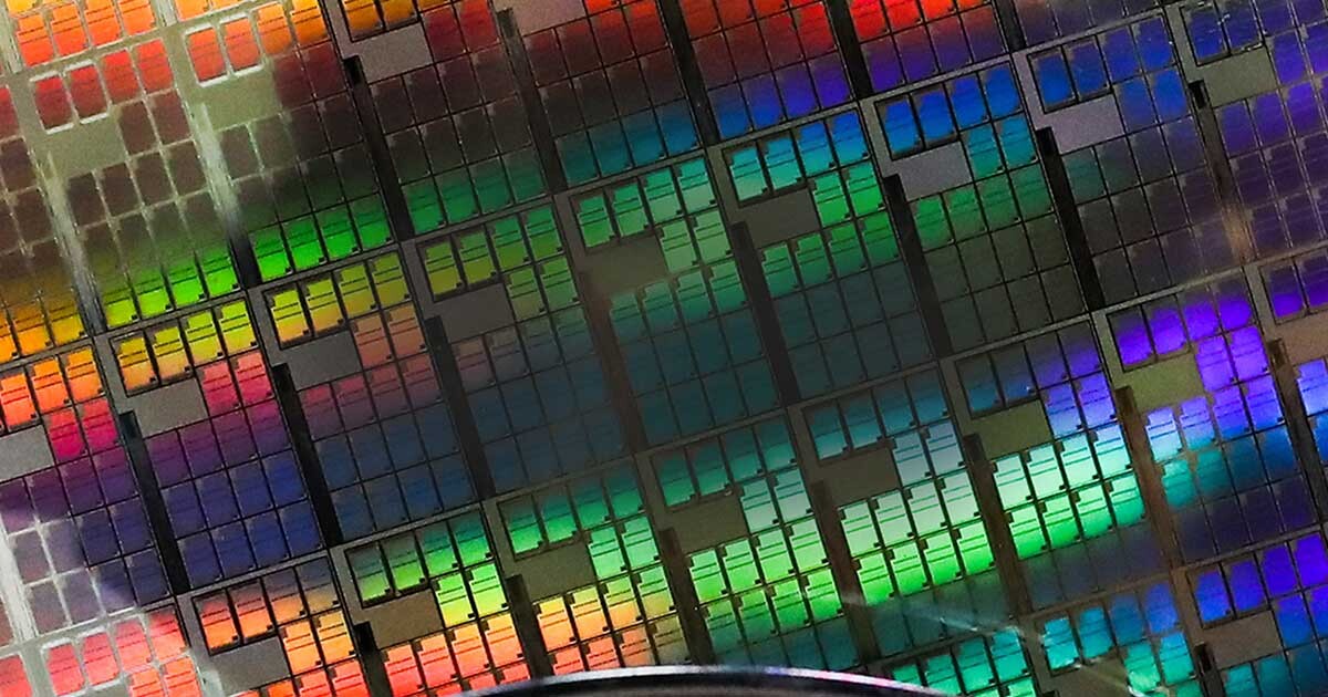
TSMC is working on a new advanced chip packaging technology that uses rectangular panel-like substrates instead of the traditional circular wafers, according to a Nikkei report citing sources. This new approach would allow more chips to be placed on a single substrate. TSMC is reportedly experimenting with rectangular substrates measuring 515 mm by 510 mm, providing more than three times the usable area compared to current 12-inch wafers. Using a rectangular-shaped wafer can potentially eliminate more of the incomplete chips found on the edges of current circular ones. While this may sound simple, it would actually require a radical change to the entire manufacturing process.

While the research is still in its early stages and may take several years to reach mass production, it represents a major technological shift for TSMC. The company has responded to Nikkei's inquiry by stating that they are closely monitoring advancements in advanced packaging technologies, including panel-level packaging. This development could potentially give TSMC an edge in meeting future chip demands, however, Intel and Samsung are also testing this new approach.
Sources: TrendForce, Nikkei
Add your own comment

25 Comments on TSMC Begins Experimenting with Rectangular Panel-Like Chip Packaging

#1
ARF
I guess the principle is simple - better late than never... But why ?
Posted on Reply
#2
Kasy21
ARFI guess the principle is simple - better late than never... But why ?
producing the waffers requiere the formation of a cilinder of perfect silicon oxide, it has to be atomically perfect and the easiest way of doing it is to make a cilinder and then cut it into waffers, growing a crystal in a rectangular way is more difficult and may lead to more inperfections, but now with the incrising price of semiconductors it may be profitable to doit this way
Posted on Reply
#3
DemonicRyzen666
ARFI guess the principle is simple - better late than never... But why ?
Edges lasers are recyclable.
Kasy21producing the waffers requiere the formation of a cilinder of perfect silicon oxide, it has to be atomically perfect and the easiest way of doing it is to make a cilinder and then cut it into waffers, growing a crystal in a rectangular way is more difficult and may lead to more inperfections, but now with the incrising price of semiconductors it may be profitable to doit this way
I was pretty sure the reason why they call it a "new spin" for lithography is because they spin it around when doing the lasering so, being a cylinder helps keep it balanced.
Posted on Reply
#4
Panther_Seraphin
Kasy21producing the waffers requiere the formation of a cilinder of perfect silicon oxide, it has to be atomically perfect and the easiest way of doing it is to make a cilinder and then cut it into waffers, growing a crystal in a rectangular way is more difficult and may lead to more inperfections, but now with the incrising price of semiconductors it may be profitable to doit this way
Looking at something like an H100 on a "modern" 12inch/300mm wafer your getting about 69 complete dies minus any defects. Same die on the new manufacturing setup would mean over 320 available minus defects. So if they can get the raw material cost down to a sensible level and with the movement from DUV to EUV you can experiment/invest heavily in that transition as the core machines have to be replaced/redesigned so adding the cost to work with the larger wafers makes logical sense.

Something like AMDs CCD on the current standard is getting ~900 dies on a standard wafer. Hits nearly 4000 on the new standard.

It would also be a lot more attractive to people like AMD/nVidia if they can do agreements on a per wafer basis as well
Posted on Reply
#5
Wirko
The news is about wafers for packaging, not active silicon chips. There's a big push and need to make silicon substrates bigger, several times as big than chips by surface area. If wafer remains round at 300 mm diameter, very few substrates would fit on it.
Kasy21producing the waffers requiere the formation of a cilinder of perfect silicon oxide, it has to be atomically perfect and the easiest way of doing it is to make a cilinder and then cut it into waffers, growing a crystal in a rectangular way is more difficult and may lead to more inperfections, but now with the incrising price of semiconductors it may be profitable to doit this way
I think that silicon ingots will continue to be made as cylinders. The technology is well established, although a significantly larger diameter of ~720 mm will be a large hurdle to overcome. They will be cut into rectangles after slicing into wafers, or maybe before that.
DemonicRyzen666they spin it around when doing the lasering
What do you mean by "lasering" here?
Posted on Reply
#6
Bones
WirkoThe news is about wafers for packaging, not active silicon chips. There's a big push and need to make silicon substrates bigger, several times as big than chips by surface area. If wafer remains round at 300 mm diameter, very few substrates would fit on it.


I think that silicon ingots will continue to be made as cylinders. The technology is well established, although a significantly larger diameter of ~720 mm will be a large hurdle to overcome. They will be cut into rectangles after slicing into wafers, or maybe before that.


What do you mean by "lasering" here?
Lithography of the chip.
That's what used to make all the little circuits, transistors and so on in silicon so it works.
Posted on Reply
#7
kondamin
So gas deposition on a square substrate like they grow diamonds?
Posted on Reply
#9
Tomorrow
About time. This has been asked many time before. Clearly rectangular chips are most efficient. Only wafers themselves are circular.
Actually you can already see rectangular wafers from the Cerebras wafer scale chip. Im not sure if it's cut from a circular one as i haven't looked into it but it should give a visual representation of what a rectangular wafer would look like. It's smaller at 215x215 compared to the 515x510 mentioned in the article.


This coupled with advancements like backside power delivery, High-NA etc should ensure continues yields into the 1.x nm era.
Posted on Reply
#10
ARF
WirkoThe news is about wafers for packaging, not active silicon chips. There's a big push and need to make silicon substrates bigger, several times as big than chips by surface area. If wafer remains round at 300 mm diameter, very few substrates would fit on it.
So, monolithic designs will not benefit from this?
Is the lack of this technology at present the reason for AMD's Navi 4C chiplet design failure?


www.techpowerup.com/312364/amd-navi-4c-gpu-detailed-shader-engines-are-their-own-chiplets?cp=2
Posted on Reply
#11
Nomad76
News Editor
TomorrowAbout time. This has been asked many time before. Clearly rectangular chips are most efficient. Only wafers themselves are circular.
Actually you can already see rectangular wafers from the Cerebras wafer scale chip. Im not sure if it's cut from a circular one as i haven't looked into it but it should give a visual representation of what a rectangular wafer would look like. It's smaller at 215x215 compared to the 515x510 mentioned in the article.
It is cut from a round wafer (www.cerebras.net/blog/cerebras-architecture-deep-dive-first-look-inside-the-hw/sw-co-design-for-deep-learning)
Posted on Reply
#12
Tomorrow
I very much doubt RDNA 4's high end ever run into design problems.
It is far more likely and logical that AMD simply sacrificed high end RDNA 4 design to give the limited CoWoS allocation to MI3XX series.

Once TSMC expands it's capacity and the AI hype dies down RDNA 5 can hopefully use CoWoS again in 2026.
I would hate consumer GPU's to be stuck with monolithic designs the same way they are restricted to GDDR memory with HBM reserved for enterprise use only.
Posted on Reply
#13
ARF
TomorrowI very much doubt RDNA 4's high end ever run into design problems.
It is far more likely and logical that AMD simply sacrificed high end RDNA 4 design to give the limited CoWoS allocation to MI3XX series.
Once TSMC expands it's capacity and the AI hype dies down RDNA 5 can hopefully use CoWoS again in 2026.
Bad forecasting and decision making back when RDNA 4 was first put as a new project.
You know that when you plan such a design, you must be well aware how you will make it in the reality.
TomorrowI would hate consumer GPU's to be stuck with monolithic designs the same way they are restricted to GDDR memory with HBM reserved for enterprise use only.
The thing is that there is no evidence that HBM in any form would help. Actually, there are other solutions - narrow memory buses, with large L3 caches (Infinity Cache), and cheapest available GDDR.
You have a problem with the shaders' utilisation, and the efficient usage of the available memory bandwidth.
You can put a 2-3TB/s memory communication, but if the shaders can feed them to only 30%, then you simply waste resources.
Posted on Reply
#14
Legacy-ZA
And you can be sure, as a custom... consumer* you will see non of those cost savings.
Posted on Reply
#15
user556
Okay, so they're actually talking about low grade wafer production for fabricating silicon interposers. Using the term "substrate" is just confusing as hell because substrate now has three different meanings within popular news of chip production.
Posted on Reply
#16
kondamin
Legacy-ZAAnd you can be sure, as a custom... consumer* you will see non of those cost savings.
Yes you will prices won't go up as much.

OTH, most consumers would be fine on 10 year old hardware, and a chip specked like those now costs $50 (intel n100)
Posted on Reply
#17
Noci
This tech level is way over my head and this may sound stupid, but why dont they use hexavalent chips to maximize the surface of circular wafers, it would make more sense to me than developing a whole new wafer design manufactering procedure with all of it's developing problems.

Anyway if this new technique does work and makes it into mass production, competition will make the prices fluctuate in comsumers benefit after a while for sure it's just market forces.
Posted on Reply
#18
Kasy21
NociThis tech level is way over my head and this may sound stupid, but why dont they use hexavalent chips to maximize the surface of circular wafers, it would make more sense to me than developing a whole new wafer design manufactering procedure with all of it's developing problems.

Anyway if this new technique does work and makes it into mass production, competition will make the prices fluctuate in comsumers benefit after a while for sure it's just market forces.
probably because it would be cheaper to change the waffer and not the chip desings, it would mean that every desingner would have to make from then on hexagonal chips so they would have to develope a new architecture from the gound up, and still they would have some loses, even if they made it hexagonal, you would also have to redesing the chip making machine, and that is always a big no no in this industry
Posted on Reply
#19
kondamin
NociThis tech level is way over my head and this may sound stupid, but why dont they use hexavalent chips to maximize the surface of circular wafers, it would make more sense to me than developing a whole new wafer design manufactering procedure with all of it's developing problems.

Anyway if this new technique does work and makes it into mass production, competition will make the prices fluctuate in comsumers benefit after a while for sure it's just market forces.
try cutting a number of hexagons out of a parent shape without damaging the hexagons.
compare that to cutting out squares of equal size
Posted on Reply
#20
Wirko
kondamintry cutting a number of hexagons out of a parent shape without damaging the hexagons.
compare that to cutting out squares of equal size
What would be the parent shape here? It's not like wafers are made from panes similar to LCD display glass.
user556Okay, so they're actually talking about low grade wafer production for fabricating silicon interposers. Using the term "substrate" is just confusing as hell because substrate now has three different meanings within popular news of chip production.
Yeah, true. I too said substrate, and I consider a substrate to be passive, while an interposer can be either passive or active.
To make things more complicated, even a Si interposer has its own substrate (the word means "bottom layer"), upon which layers with wires are built.
ARFThe thing is that there is no evidence that HBM in any form would help. Actually, there are other solutions - narrow memory buses, with large L3 caches (Infinity Cache), and cheapest available GDDR.
Agreed. HBM is for those who need, and can pay for, very high density and lower consumption (in joules/bit). That's how you stuff 100 or 200 AMD or NV accelerators in a single rack.
Nomad76I can be way-off so I'm just assuming they may also switch from the Czochralski process (resulting in cylindrical silicon ingots) to the Bridgman-Stockbarger horizontal method that produced some D-shaped ingots. Rectangular wafers are used mainly for solar panels..
Hm, that's possible, yes, as Si substrates without transistors don't demand the highest purity crystals or best uniformity.
Posted on Reply
#21
kondamin
WirkoWhat would be the parent shape here? It's not like wafers are made from panes similar to LCD display glass.
Doesn't matter what shape it's cut from, slicing them out is a lot harder than it is doing the same with rectangular chips
*first wafer i found googling no clue what's on it.


you would need a very precise cutting machine to not damage the other tiles as the cutting thing would have to go right over them
Posted on Reply
#22
Wirko
kondaminDoesn't matter what shape it's cut from, slicing them out is a lot harder than it is doing the same with rectangular chips
*first wafer i found googling no clue what's on it.


you would need a very precise cutting machine to not damage the other tiles as the cutting thing would have to go right over them
I misunderstood the idea, it was about making hexagonal chips from round wafers, not hexagonal wafers from a giant pane.

But whatever the process is, the cost of the discarded, unexposed parts of the wafer should be vastly lower than the cost of fully processed parts, that is, the dice, or dies. Semianalysis had an article with costs breakdown but I can't find it right now.

So maybe the waste is a small issue really - until your substrates become very big compared to 300 mm.
Posted on Reply
#23
Xajel
DemonicRyzen666Edges lasers are recyclable.


I was pretty sure the reason why they call it a "new spin" for lithography is because they spin it around when doing the lasering so, being a cylinder helps keep it balanced.
True, but the original silicon ingot that wafers are sliced from is cylindrical, this is how it was manufactured in the first place, doing it in a rectangular shape not only means different manufacturing but different processing in the whole chip-making process, including different machines and robots.

This is how the silicon ingot looks, and after being sliced.

Posted on Reply
#24
user556
I'm pretty certain this news item is about packaging alone - making interposers in particular. ie: The rectangular wafers are not for making dies.
Posted on Reply
#25
Chrispy_
user556I'm pretty certain this news item is about packaging alone - making interposers in particular. ie: The rectangular wafers are not for making dies.
Yeah, that's how I interpret it too.

The actual die wafers are still going to be round, because they're sliced pure silicon crystals. You don't get to choose the shape of the crystals, that's predetermined by the polarity and bond arrangement of silicon atoms.
Posted on Reply
Add your own comment
Jun 29th, 2024 22:45 EDT change timezone

New Forum Posts

Popular Reviews

Controversial News Posts