 348
348
AMD Radeon R9 Fury X 4 GB Review
Test Setup »A Closer Look
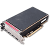
AMD's cooling solution is a little technology marvel. It is made by Cooler Master and integrates waterblock, pump, and VRM cooling circuitry in one piece.
The next piece that goes off is the metal backplate, which helps protect the card against damage during handling, while adding to the product's visuals.
After removing the Radeon shroud (which is lit, by the way), we get to take a closer look at the watercooling components.
Note the piece of copper tubing that runs along the right side of the GPU. It cools the voltage regulation circuitry below it, an elegant solution. Other designs use a fan for that, which would add extra noise.
With the waterblock removed, we can finally get a first glimpse of the GPU, which is still covered by A LOT of thermal paste. The waterblock uses a copper baseplate with a milled-out section for the GPU; there is no additional milling for the HBM chips.
The radiator is your typical 120 mm variant, with a very quiet fan made by Nidec.
A row of LEDs will indicate the GPU's power draw, acting as the GPU's activity indicator. The left-most LED is green and will light up when the card is running in ZeroCore power mode (the pump and fan will not turn off in ZeroCore). You may change the color using the DIP switches to the left.
Like on most recent AMD Radeon products, a dual-BIOS switch is included, which serves as a fail-safe in case a BIOS flash goes wrong. The two BIOSes are identical.
Power delivery requires two 8-pin PCI-Express power connectors. This configuration is specified for up to 375 W power draw.
We've seen the IR 3567 voltage controller on the R9 390x/290X before. It supports software voltage control and monitoring via I2C and is well supported in overclocking software.
The HBM memory chips are by Hynix. They are specified to run at 500 MHz. The two stacks pictured in the photo are each comprised of five stacked silicon dies, four DRAM and one controller. A total of four stacks are installed, sitting on the silicon interposer (the colorful parts), together with the large GPU die.
AMD's Fiji graphics processor uses the GCN shader architecture. It is produced on a 28 nm process at TSMC, Taiwan, with 8.9 billion transistors on a 596 mm² die.
May 5th, 2025 04:20 EDT
change timezone
Latest GPU Drivers
New Forum Posts
- Best USB 3 hub chipsets (22)
- [AV1, AV2, AV3 codecs...] Have they given up on the AOMedia project? (16)
- RX 9000 series GPU Owners Club (640)
- Low budget psu for medium high loads (under 400 watt usage) (22)
- HP laptop upgrade ZBook G2 k4100 to Nvidia GTX 1070m and EliteBook 8770 (a few laptops) (33)
- (Mis)adventures in Storage Benchmarking (NVMe, Optane, Thunderbolt) (4)
- Choosing an Internal HDD (61)
- Asus motherboard AM5 safe to buy in 2025? (15)
- Post your Speedtest.net Speeds! (2360)
- It's happening again, melting 12v high pwr connectors (1053)
Popular Reviews
- ASUS ROG Maximus Z890 Hero Review
- ASUS Radeon RX 9070 XT TUF OC Review
- Clair Obscur: Expedition 33 Performance Benchmark Review - 33 GPUs Tested
- Montech HS02 PRO Review
- NVIDIA GeForce RTX 5060 Ti 8 GB Review - So Many Compromises
- Seasonic Vertex GX 850 W Review
- Upcoming Hardware Launches 2025 (Updated Apr 2025)
- ASUS GeForce RTX 5090 Astral Liquid OC Review - The Most Expensive GPU I've Ever Tested
- Sapphire Radeon RX 9070 XT Nitro+ Review - Beating NVIDIA
- AMD Ryzen 7 9800X3D Review - The Best Gaming Processor
Controversial News Posts
- AMD Radeon RX 9060 XT to Roll Out 8 GB GDDR6 Edition, Despite Rumors (129)
- NVIDIA Sends MSRP Numbers to Partners: GeForce RTX 5060 Ti 8 GB at $379, RTX 5060 Ti 16 GB at $429 (128)
- NVIDIA Launches GeForce RTX 5060 Series, Beginning with RTX 5060 Ti This Week (115)
- Nintendo Confirms That Switch 2 Joy-Cons Will Not Utilize Hall Effect Stick Technology (105)
- NVIDIA PhysX and Flow Made Fully Open-Source (95)
- Sony Increases the PS5 Pricing in EMEA and ANZ by Around 25 Percent (84)
- Parts of NVIDIA GeForce RTX 50 Series GPU PCB Reach Over 100°C: Report (78)
- Intel "Bartlett Lake-S" Gaming CPU is Possible, More Hints Appear for a 12 P-Core SKU (77)


