 348
348
AMD Radeon R9 Fury X 4 GB Review
(348 Comments) »Introduction
To say that AMD is at the forefront of new technology in the PC-graphics field is an understatement. The company rigorously pursues and in many cases introduces new technology into the PC consumer-graphics space. AMD's past two memorable technological breakthroughs in this space were Graphics CoreNext, a powerful new number-crunching machinery for the GPU, which made not just AMD, but also a lot of crypto-currency enthusiasts a lot of money, and the first GPU with GDDR5 memory in their giant-killing Radeon HD 4870. The past year hasn't been kind to AMD in terms of GPU-market share, which is partly because the company didn't introduce anything major since 2013; all due to competition from NVIDIA with its "Maxwell" architecture and probably also because the company is focusing on high-volume ISV deals, such as new-generation game consoles, and the development of the chip we're reviewing today, the Radeon R9 Fury X.
The R9 Fury X is not a case of AMD taking its existing tech and up-scaling it. The company probably can't do that anymore. AMD and NVIDIA's common foundry partner for GPUs, TSMC, has seen major setbacks in implementing its next silicon fabrication tech, which threw both companies' product-development cycles off the track. While it hit NVIDIA hard, which had to rework its "Maxwell" architecture for the existing 28 nm process, it hit AMD harder. The company was already hitting 275W TBP (typical board power) with its previous-gen high-end chip, the R9 290X, and making the kind of SIMD increase that it did with its new chip could have adversely affected TBP. The card has the same exact TBP as the R9 290X at 275W, but at a whopping 45% increase in its number-crunching machinery. So AMD has obviously done something very big with the physically very small R9 Fury X - High Bandwidth Memory (HBM).
Stacked High Bandwidth Memory (HBM) is the biggest innovation in video card memory since GDDR5 (circa summer 2008). It is complemented by a transfer of video memory from physical chips surrounding the GPU package - over 32-bit-wide data paths, each. More on this later.
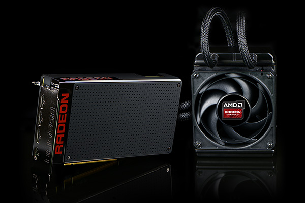
The Radeon R9 290 and R9 290X hit NVIDIA's high-end GPU lineup back in fall-2013. The $399 R9 290 was faster than the $999 GTX TITAN and the $650 GTX 780; while the R9 290X held out on its own until NVIDIA made a product intervention with the GTX 780 Ti and GTX TITAN Black to reclaim those two price points. That didn't affect AMD's competitiveness until NVIDIA launched the "Maxwell" based GTX 970 and GTX 980. Some of the major complaints with the R9 290/X were that it was very hot and noisy. We dreaded the prospect of a dual-GPU card based on the "Hawaii" silicon, but were pleasantly surprised when the dual-GPU R9 295X2 turned out to be cooler and quieter than single-GPU NVIDIA chips. It could do so because AMD tapped into liquid cooling. The card shipped with a factory-fitted, close-loop liquid cooler. Close-loop liquid coolers for CPUs were taking off around the same time, and so the two-piece contraption strung together by coolant tubes didn't really affect the product's standing with buyers. NVIDIA launching a prohibitively expensive GTX TITAN-Z helped too. Given the Radeon Fury X has the same board-power rating as the R9 290X, AMD also gave it a liquid-cooling solution in an effort to clinch the heat-and-noise game against NVIDIA's high-end "Maxwell" GPUs, including the GTX Titan X and the more recently launched GTX 980 Ti.
AMD is pricing the Radeon Fury X at US $650. This and $550 have traditionally been the price-points at which AMD launches its high-end, single-GPU products. NVIDIA prepared for this product launch by introducing the GTX 980 Ti at $650, based on the same silicon as the GTX Titan X, and cutting pricing of the $550 GTX 980 down to $500. The Radeon R9 Fury X has its task cut out for itself in repeating the R9 290 series launch in which the biggest winner was the consumer.
| Radeon R9 390X | GeForce GTX 780 Ti | GeForce GTX 980 | Radeon Fury X | GeForce GTX 980 Ti | GeForce GTX Titan X | Radeon R9 295X2 | |
|---|---|---|---|---|---|---|---|
| Shader Units | 2816 | 2880 | 2048 | 4096 | 2816 | 3072 | 2x 2816 |
| ROPs | 64 | 48 | 64 | 64 | 96 | 96 | 2x 64 |
| Graphics Processor | Hawaii | GK110 | GM204 | Fiji | GM200 | GM200 | 2x Hawaii |
| Transistors | 6200M | 7100M | 5200M | 8900M | 8000M | 8000M | 2x 6200M |
| Memory Size | 8192 MB | 3072 MB | 4096 MB | 4096 MB | 6144 MB | 12288 MB | 2x 4096 MB |
| Memory Bus Width | 512 bit | 384 bit | 256 bit | 4096 bit | 384 bit | 384 bit | 2x 512 bit |
| Core Clock | 1050 MHz | 876 MHz+ | 1126 MHz+ | 1050 MHz | 1000 MHz+ | 1000 MHz+ | 1018 MHz |
| Memory Clock | 1500 MHz | 1750 MHz | 1750 MHz | 500 MHz | 1750 MHz | 1750 MHz | 1250 MHz |
| Price | $430 | $390 | $480 | $650 | $650 | $1050 | $620 |
Architecture
At the heart of the Radeon R9 Fury X is the most talked about GPU of the season, codenamed "Fiji." It is a multi-chip module of three important components - the GPU die itself, built on TSMC's 28 nm process, a specially designed silicon substrate layer that seats and connects the GPU die with the HBM memory stacks, called interposer and built by UMC on its 65 nm process, and four 1 GB HBM stacks made by SK Hynix on a 20 nm-class node. AMD had technical assistance from some of the industry's brightest VLSI teams, including from UMC, Amkor Technology, ASE Group, and SK Hynix.Let's begin with the GPU die itself. It features a familiar component hierarchy to the previous-generation "Hawaii" silicon. The Graphics CoreNext stream processors, however, are of a newer generation, GCN 1.2, which made its debut with the "Tonga" silicon that powers the Radeon R9 380 and R9 285.
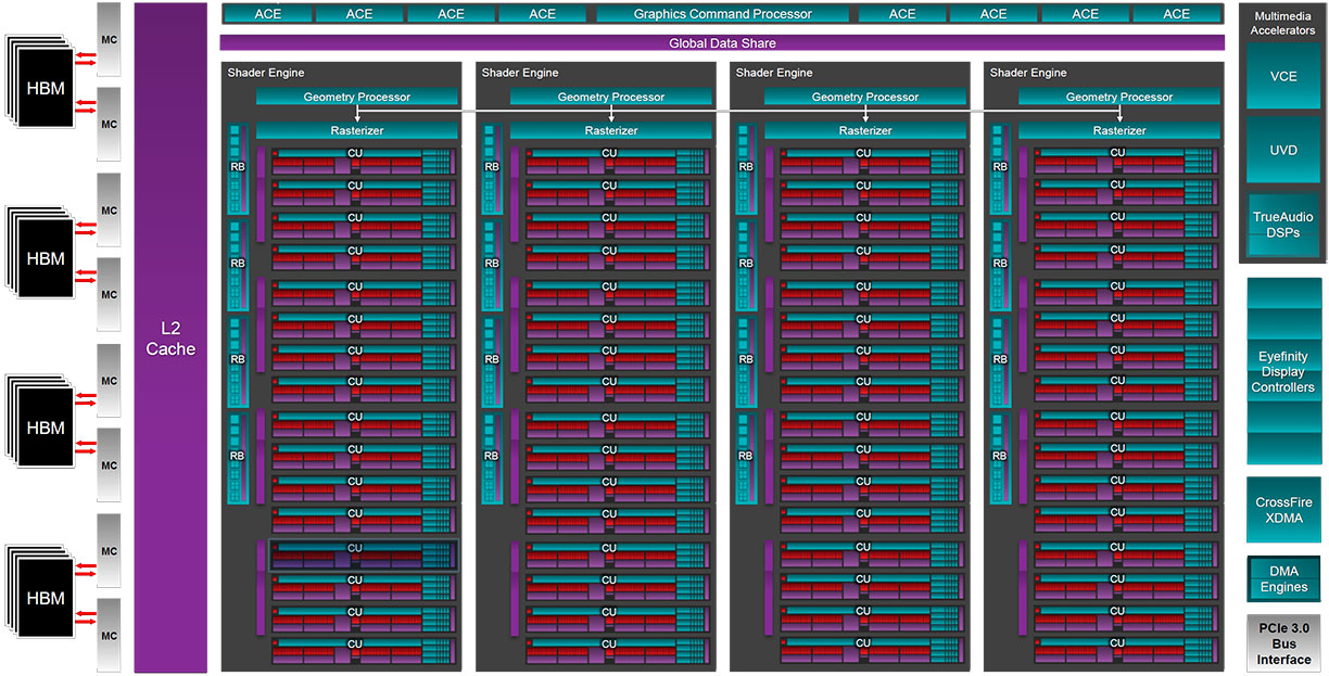
The GPU die features four shader engines, just like "Hawaii," but the compute unit (CU) count per shader engine has been increased to 16 from the 11 on "Hawaii." Each CU packs 64 stream processors, so there are 1,024 stream processors per engine and 4,096 on the chip in total. There are 16 render back-ends, which is the same as in "Hawaii," so the ROP count remains the same at 64. The higher CU count, however, means that the TMU count is at 256 instead of the 176 on "Hawaii." The biggest change, however, is the 4096-bit wide HBM interface which wires out to four 8 Gigabit HBM stacks.
AMD didn't announce any changes to the ancillaries - the multimedia engine, XDMA CrossFire (no bridge cables required), display controllers with support for DisplayPort 1.2a and HDMI 1.4a, and PCI-Express gen 3.0 x16 host interface remain the same as on "Hawaii." There is one notable change, though, since the reference design card lacks DVI connectors. It features three DP 1.2a and one HDMI ports. All ports are on the first slot elevation, making this card truly single-slot capable with aftermarket liquid-cooling blocks (the piggybacked DVI connector that extends into the second slot denies NVIDIA cards this cool feature unless you're skillful enough to solder out the DVI connector without accidentally shorting any pins).
High Bandwidth Memory and Interposer
With Windows 10 and its companion DirectX 12 API on the horizon, and high display resolutions such as 1440p and 4K Ultra HD getting increasingly more affordable - 1440p displays start at $250 and 4K starts at $400 if you know where to look - the demands on video memory to catch up have never been higher. GDDR5 served the industry well since its debut in 2008. It has driven five generations of GPUs since, but is approaching its design limitation for performance upscaling through clock-speed increases.
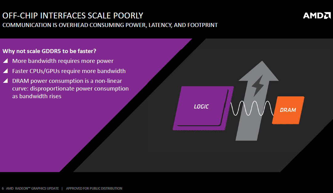
For any memory standard (including HBM), memory speed/bandwidth and power draw don't scale linearly. Beyond a point, the equation tapers too much in favor of power requirements, and so, an increasingly disproportionate amount of power is required to achieve higher clocks. This is what necessitates a new memory standard. HBM is just starting out on that same curve, and hence, has much better energy efficiency than GDDR5. HBM trades frequency for bus-width and offers vertical stacking of DRAM dies. This generation of HBM allows vertical stacking of up to four DRAM dies, with a fifth logic die holding the PHY and connections out of the stack.
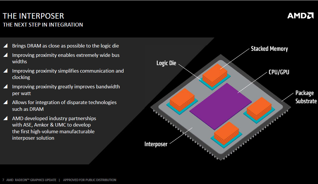
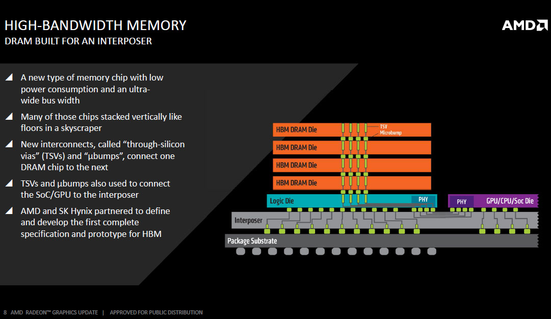
The Fiji package features four 8 Gb HBM stacks, each with 1,024-bit wide memory bus. Since such a wide bus per stack would take up an obscene number of pins on a standalone memory chip package, AMD decided to integrate it into the GPU package, using a specially designed substrate called the interposer to deal with the wiring problem.
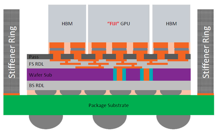
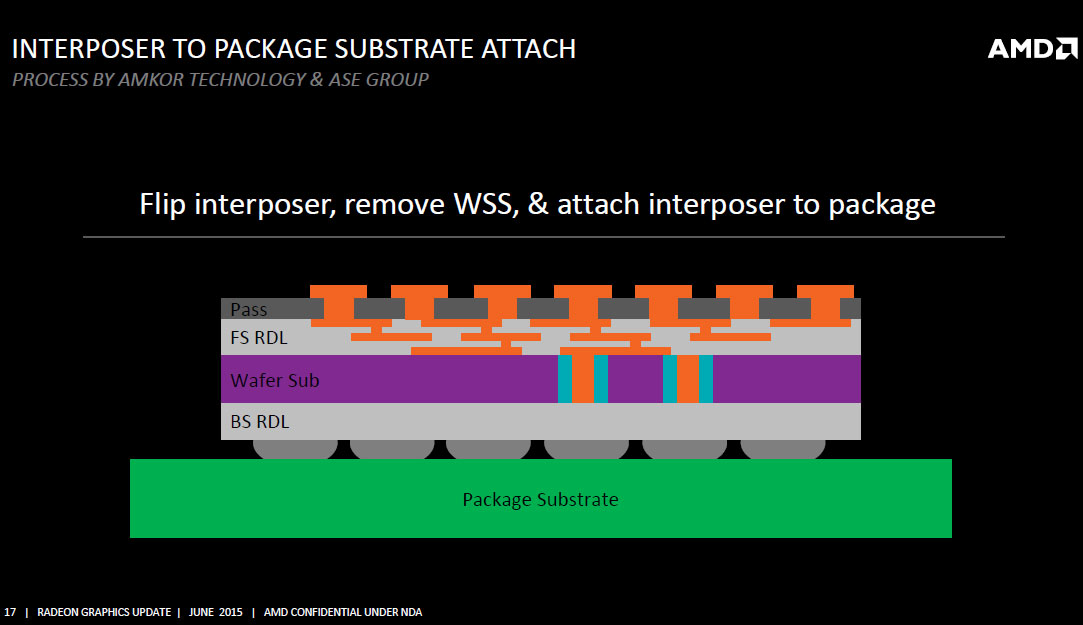
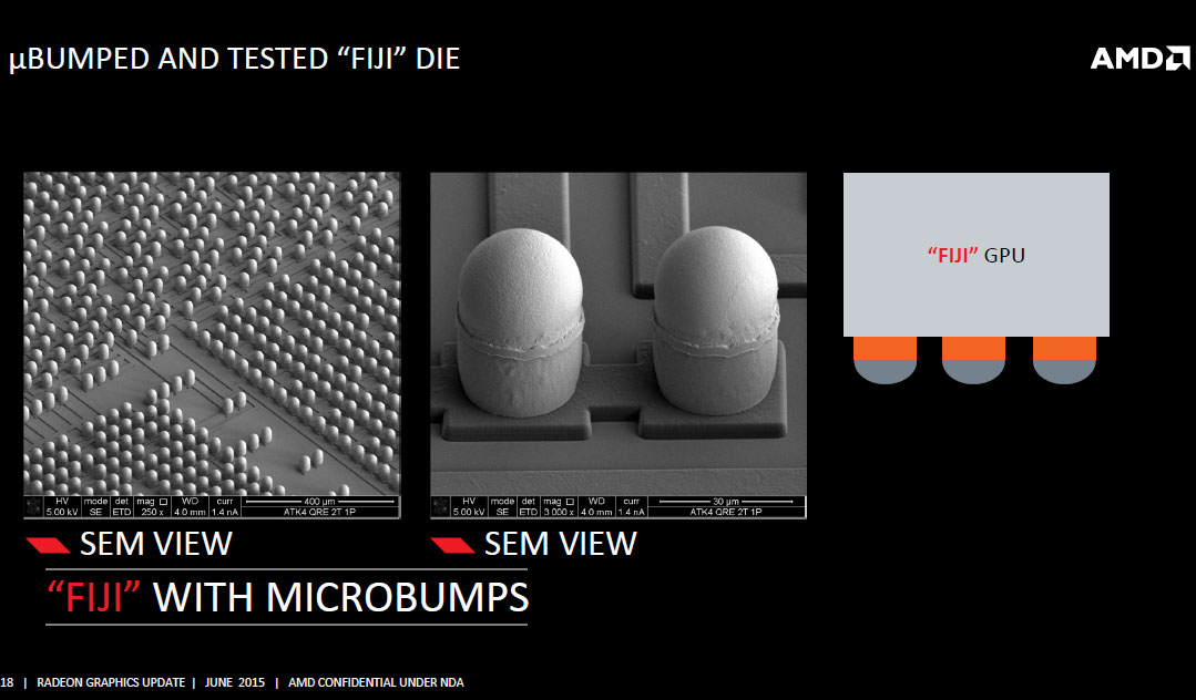
The interposer is essentially a very large silicon die that acts as a substrate for other dies. There's no number crunching or storage happening here as there is just a vast network of microscopic wires running between the HBM stacks and the GPU die. The interposer is built on a 65 nanometer silicon fab node. It may not sound like much in the 20 nm-class era, but compared to conventional fiberglass PCB wiring, wires on the 65 nm node are infinitesimally smaller, as are bumps, points of contact between two dies or between a die and a substrate. AMD innovated microscopic bumps specifically for contact between the GPU die and the interposer because wiring between the GPU and the memory is just so dense.
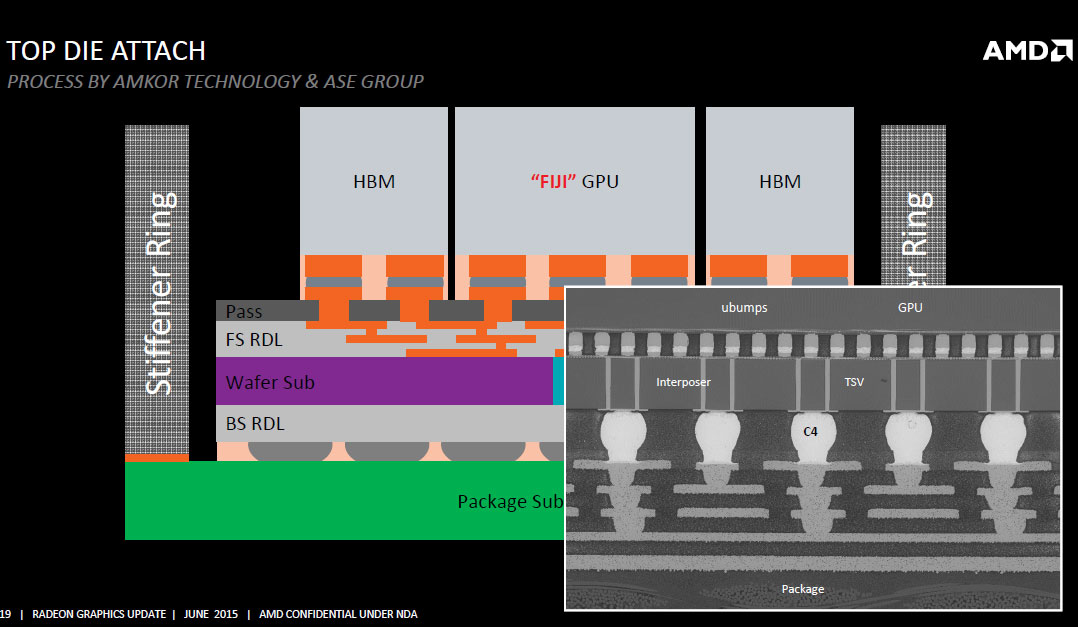
The interposer has microscopic bumps on the side that faces toward the GPU die and HBM stacks and conventional bumps, also on the side, that face toward the main fiberglass substrate of the GPU package. With the memory moved to the GPU package, and more importantly, the most sensitive wiring of the video card (that between the memory and GPU) moved to the GPU package, there's not much action on the PCB. The pins on the package are for power, system bus, and display I/O, which gives AMD greater quality control.

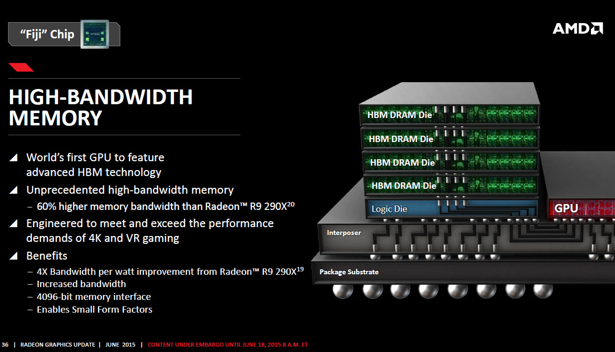
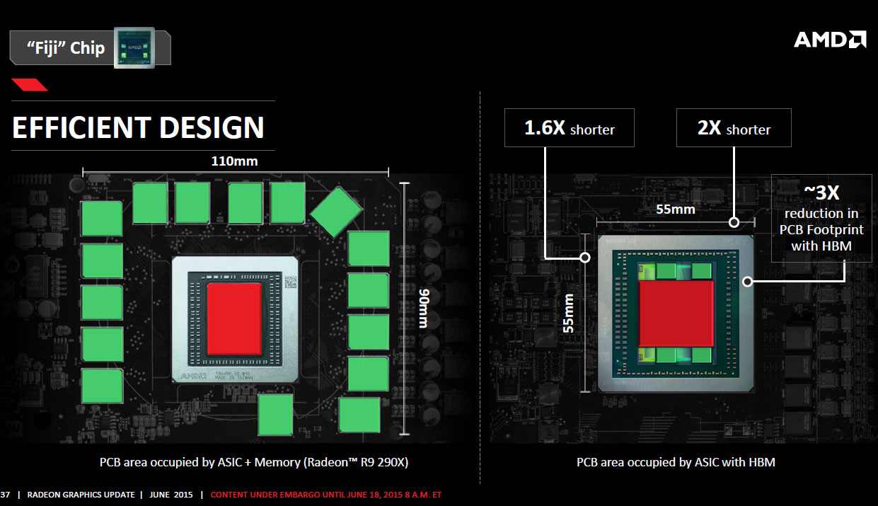
Another major benefit of moving the memory to the GPU package, however, is the savings in PCB real-estate. Sure, the package in itself is bigger than "Hawaii" or any GPU ever made, but since there are no memory chips surrounding it, all that's left on the video card's PCB are the GPU package, VRM, and display I/O. This allows AMD to create some extremely compact products. The reference PCB of the Radeon R9 Fury X is just 19 cm long. Dual GPU video card PCBs made using this chip will be smaller than even single-GPU cards made using "Hawaii," which should also benefit notebook MXM designers.
Packaging
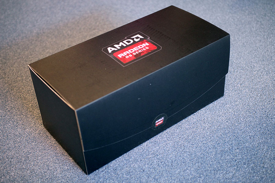
We've received our sample in a box specifically crafted by AMD for review purposes.
Final retail cards will come with the usual accessories, like driver CD, adapters, and power cables.
Our Patreon Silver Supporters can read articles in single-page format.
Apr 13th, 2025 19:19 EDT
change timezone
Latest GPU Drivers
New Forum Posts
- GCN less stable on AM4 than 2011-3? (2)
- Gigabyte 5090 Aorus Master VRM Specs (20)
- What is going to be your next tech upgrade? just curious :) (40)
- AMD Radeon RX 7900 XTX overclocking (0)
- What local LLM-s you use? (157)
- Why PC Gaming rocks (11)
- Radeon RX 6700, 6700 XT & 6750 XT users club (1130)
- Lian Li O11 Dynamic XL ROG. (11)
- Regarding fan noise (10)
- Advice on GPU upgrade (12)
Popular Reviews
- Thermaltake TR100 Review
- The Last Of Us Part 2 Performance Benchmark Review - 30 GPUs Compared
- TerraMaster F8 SSD Plus Review - Compact and quiet
- ASUS GeForce RTX 5080 TUF OC Review
- Zotac GeForce RTX 5070 Ti Amp Extreme Review
- Sapphire Radeon RX 9070 XT Pulse Review
- ASRock Z890 Taichi OCF Review
- Sapphire Radeon RX 9070 XT Nitro+ Review - Beating NVIDIA
- Upcoming Hardware Launches 2025 (Updated Apr 2025)
- AMD Ryzen 7 9800X3D Review - The Best Gaming Processor
Controversial News Posts
- NVIDIA GeForce RTX 5060 Ti 16 GB SKU Likely Launching at $499, According to Supply Chain Leak (181)
- MSI Doesn't Plan Radeon RX 9000 Series GPUs, Skips AMD RDNA 4 Generation Entirely (146)
- Microsoft Introduces Copilot for Gaming (124)
- NVIDIA Sends MSRP Numbers to Partners: GeForce RTX 5060 Ti 8 GB at $379, RTX 5060 Ti 16 GB at $429 (124)
- Nintendo Confirms That Switch 2 Joy-Cons Will Not Utilize Hall Effect Stick Technology (105)
- Over 200,000 Sold Radeon RX 9070 and RX 9070 XT GPUs? AMD Says No Number was Given (100)
- Nintendo Switch 2 Launches June 5 at $449.99 with New Hardware and Games (99)
- NVIDIA PhysX and Flow Made Fully Open-Source (77)