 341
341
AMD Radeon RX 7600 Review - For 1080p Gamers
Test Setup »High-resolution PCB Pictures
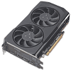
These pictures are for the convenience of volt modders and people who would like to see all the finer details on the PCB. Feel free to link back to us and use these in your articles, videos or forum posts.High-resolution versions are also available (front, back).
Circuit Board (PCB) Analysis
GPU voltage is an 8-phase design, managed by a IRF 35217 controller.
GPU voltage on AMD is two separate rails. On one, OnSemi NCP302155 DrMOS chips with a 55 A rating are used, the other rail uses OnSemi NCP302045 chips with a 45 A rating.
Memory voltage uses a two-phase design and is generated by an NCP81022N controller.
For memory, 45 A OnSemi NCP302045 DrMOS chips are used.
The GDDR6 memory chips are made by Hynix and carry the model number H56G42AS8DX-014. They are specified to run at 2500 MHz (20 Gbps effective).
AMD's new Navi 33 graphics processor is a monolithic design, unlike Navi 31, which powers the RX 7900 Series. It is fabricated on a 6 nm process at TSMC Taiwan with a die size of 204 mm² and 13.3 billion transistors.
Mar 10th, 2025 04:50 EDT
change timezone
Latest GPU Drivers
New Forum Posts
- RTX 5090 ridiculous price! (188)
- Nvidia's GPU market share hits 90% in Q4 2024 (gets closer to full monopoly) (761)
- RX 9070 availability (115)
- What are you playing? (23121)
- RX 9000 series GPU Owners Club (32)
- As we live the age of game remakes, which game you would like to see to have a remake? (356)
- 9070 XT - 2x HDMI high refresh displays (144 and 120 Hz) not working (13)
- *Severe micro stutters* cyberpunk 2077 Please help (57)
- Post your Monster Hunter Wilds benchmark scores (144)
- EVGA RTX 3060 XC 12gb wrong bios device id mismatch (4)
Popular Reviews
- Sapphire Radeon RX 9070 XT Nitro+ Review - Beating NVIDIA
- XFX Radeon RX 9070 XT Mercury OC Magnetic Air Review
- ASUS Radeon RX 9070 TUF OC Review
- MSI MAG B850 Tomahawk Max Wi-Fi Review
- NVIDIA GeForce RTX 5080 Founders Edition Review
- NVIDIA GeForce RTX 5070 Founders Edition Review
- Corsair Vengeance RGB CUDIMM DDR5-8800 48 GB CL42 Review
- AMD Ryzen 7 9800X3D Review - The Best Gaming Processor
- ASUS GeForce RTX 5070 Ti TUF OC Review
- MSI GeForce RTX 5070 Ti Gaming Trio OC+ Review
Controversial News Posts
- NVIDIA GeForce RTX 50 Cards Spotted with Missing ROPs, NVIDIA Confirms the Issue, Multiple Vendors Affected (513)
- AMD Plans Aggressive Price Competition with Radeon RX 9000 Series (277)
- AMD Radeon RX 9070 and 9070 XT Listed On Amazon - One Buyer Snags a Unit (261)
- AMD RDNA 4 and Radeon RX 9070 Series Unveiled: $549 & $599 (260)
- AMD Mentions Sub-$700 Pricing for Radeon RX 9070 GPU Series, Looks Like NV Minus $50 Again (248)
- NVIDIA Investigates GeForce RTX 50 Series "Blackwell" Black Screen and BSOD Issues (244)
- AMD Radeon RX 9070 and 9070 XT Official Performance Metrics Leaked, +42% 4K Performance Over Radeon RX 7900 GRE (195)
- AMD Radeon RX 9070-series Pricing Leaks Courtesy of MicroCenter (158)


