 135
135
AMD Radeon RX 7900 XT Review
Test Setup »High-resolution PCB Pictures
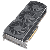
These pictures are for the convenience of volt modders and people who would like to see all the finer details on the PCB. Feel free to link back to us and use these in your articles, videos or forum posts.High-resolution versions are also available (front, back).
Circuit Board (PCB) Analysis
GPU voltage is a 14-phase design, managed by a Monolithic Power Systems MP2857 controller.
Monolithic MP87997 DrMOS components are used for GPU voltage; they are rated for 70 A of current each.
Memory voltage is a three-phase design, managed by a Monolithic Power Systems MP2856 controller.
For memory, Monolithic MP87997 DrMOS with a 70 A rating are used again.
As mentioned before, the card has a USB-C DisplayPort-passthrough output. This chip enables that functionality, it supports USB PD 3.0,
The GDDR6 memory chips are made by Hynix and carry the model number H56G42AS8DX-014. They are specified to run at 2500 MHz (20 Gbps effective).
AMD's new Navi 31 graphics processor is the world's first GPU that uses a chiplet architecture. Note the large die in the center, called "GCD," graphics compute die, which houses the compute units, it is surrounded by six smaller "MCD," memory cache dies, that contain one memory controller interface and one slice of cache each. While they look similar, the MCDs are not HBM memory chips. The MCDs are fabricated on a 6 nm process at TSMC Taiwan with a die size of 36.6 mm² each, the GCD is fabricated using TSMC's 5 nanometer node, with a die size of 300 mm². The combined transistor count of the GPU is 57.7 billion.
As mentioned before, the XT has only five MCDs, the sixth one that you see in the photo above is a non-functional dummy die, used to stabilize and distribute the heatsink pressure.
Apr 17th, 2025 02:48 EDT
change timezone
Latest GPU Drivers
New Forum Posts
- Windows 11 General Discussion (5986)
- Your PC ATM (35358)
- Need advice RAM for Asus Maximus hero z890 + core ultra 7 265k (34)
- Windows 11 fresh install to do list (38)
- RX 9000 series GPU Owners Club (338)
- Advice for DDR5 CU-DIMM 2 x 24gb 8400mhz (32)
- How to relubricate a fan and/or service a troublesome/noisy fan. (241)
- EVGA 3070ti hotspot is too high 107.7° (10)
- Will you buy a RTX 5090? (479)
- 5070 Ti power limit questions (42)
Popular Reviews
- G.SKILL Trident Z5 NEO RGB DDR5-6000 32 GB CL26 Review - AMD EXPO
- ASUS GeForce RTX 5060 Ti TUF OC 16 GB Review
- ASUS GeForce RTX 5080 TUF OC Review
- NVIDIA GeForce RTX 5060 Ti PCI-Express x8 Scaling
- DAREU A950 Wing Review
- Palit GeForce RTX 5060 Ti Infinity 3 16 GB Review
- ASUS GeForce RTX 5060 Ti Prime OC 16 GB Review
- Zotac GeForce RTX 5060 Ti AMP 16 GB Review
- The Last Of Us Part 2 Performance Benchmark Review - 30 GPUs Compared
- Sapphire Radeon RX 9070 XT Pulse Review
Controversial News Posts
- NVIDIA GeForce RTX 5060 Ti 16 GB SKU Likely Launching at $499, According to Supply Chain Leak (182)
- NVIDIA Sends MSRP Numbers to Partners: GeForce RTX 5060 Ti 8 GB at $379, RTX 5060 Ti 16 GB at $429 (127)
- Nintendo Confirms That Switch 2 Joy-Cons Will Not Utilize Hall Effect Stick Technology (105)
- Over 200,000 Sold Radeon RX 9070 and RX 9070 XT GPUs? AMD Says No Number was Given (100)
- Nintendo Switch 2 Launches June 5 at $449.99 with New Hardware and Games (99)
- NVIDIA Launches GeForce RTX 5060 Series, Beginning with RTX 5060 Ti This Week (92)
- Sony Increases the PS5 Pricing in EMEA and ANZ by Around 25 Percent (85)
- NVIDIA PhysX and Flow Made Fully Open-Source (77)


