 228
228
AMD Radeon RX Vega 64 8 GB Review
Test Setup »PCB Analysis
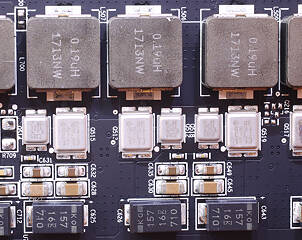
HBM memory integrates tightly with the GPU die, by sitting right next to it on the silicon package. This approach promises smaller PCB real estate usage, but AMD has opted to keep their card full size. Arranged around the GPU is almost nothing but voltage regulation circuitry, probably to keep sufficient space for the heatsink and fan.
The IR35217 voltage controller seems to be a new design for RX Vega. It feeds its six PWM phase signals into six IR 3598 phase doublers on the back side of the PCB. These six chips now drive twelve power phases, each made up of an IR6894 and IR6211.
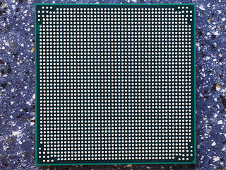
The HBM2 memory chips are made by Samsung. You see two stacks, which add up to a total memory capacity of 8 GB. If you take a closer look at the picture above, you will notice that the space between the GPU and memory chips has been filled up with a clear/gray substance. This is in contrast to the Radeon RX 56 GPU from our other review, which has an empty space here, just like we've seen on the R9 Fury X. A hint to these differences could be the "made in Taiwan" print on the GPU of Vega 64, whereas Vega 56 uses a GPU "made in Korea".
AMD's Vega 10 graphics processor is produced on a 14 nanometer process using 12 billion transistors occupying a die size of 486 mm².
Apr 7th, 2025 22:41 EDT
change timezone
Latest GPU Drivers
New Forum Posts
- is it worth using ssd with usb2? (10)
- Question about Intel Optane SSDs (70)
- USB case with dual USB-C and dual USB-A (6)
- The TPU UK Clubhouse (26058)
- Help me pick a UPS (88)
- Anyone with true HDDs still around here? (336)
- 12v lines 0 reads occansionally (2)
- Someone run games on AMD BC-250 under Linux * Cut down PS5 die to 6 CPU cores 24 GPU cores for use in crypto mining (79)
- RX 9000 series GPU Owners Club (236)
- The coffee and tea drinkers club. (246)
Popular Reviews
- The Last Of Us Part 2 Performance Benchmark Review - 30 GPUs Compared
- UPERFECT UStation Delta Max Review - Two Screens In One
- ASUS Prime X870-P Wi-Fi Review
- PowerColor Radeon RX 9070 Hellhound Review
- Upcoming Hardware Launches 2025 (Updated Apr 2025)
- Sapphire Radeon RX 9070 XT Pulse Review
- MCHOSE L7 Pro Review
- Corsair RM750x Shift 750 W Review
- Sapphire Radeon RX 9070 XT Nitro+ Review - Beating NVIDIA
- DDR5 CUDIMM Explained & Benched - The New Memory Standard
Controversial News Posts
- NVIDIA GeForce RTX 5060 Ti 16 GB SKU Likely Launching at $499, According to Supply Chain Leak (159)
- MSI Doesn't Plan Radeon RX 9000 Series GPUs, Skips AMD RDNA 4 Generation Entirely (146)
- Microsoft Introduces Copilot for Gaming (124)
- AMD Radeon RX 9070 XT Reportedly Outperforms RTX 5080 Through Undervolting (119)
- NVIDIA Reportedly Prepares GeForce RTX 5060 and RTX 5060 Ti Unveil Tomorrow (115)
- Over 200,000 Sold Radeon RX 9070 and RX 9070 XT GPUs? AMD Says No Number was Given (100)
- NVIDIA GeForce RTX 5050, RTX 5060, and RTX 5060 Ti Specifications Leak (97)
- Nintendo Switch 2 Launches June 5 at $449.99 with New Hardware and Games (92)


