 142
142
AMD Ryzen 5 8500G Review - Zen 4 + Zen 4c Tested
Socket AM5 Platform & Chipsets »Architecture
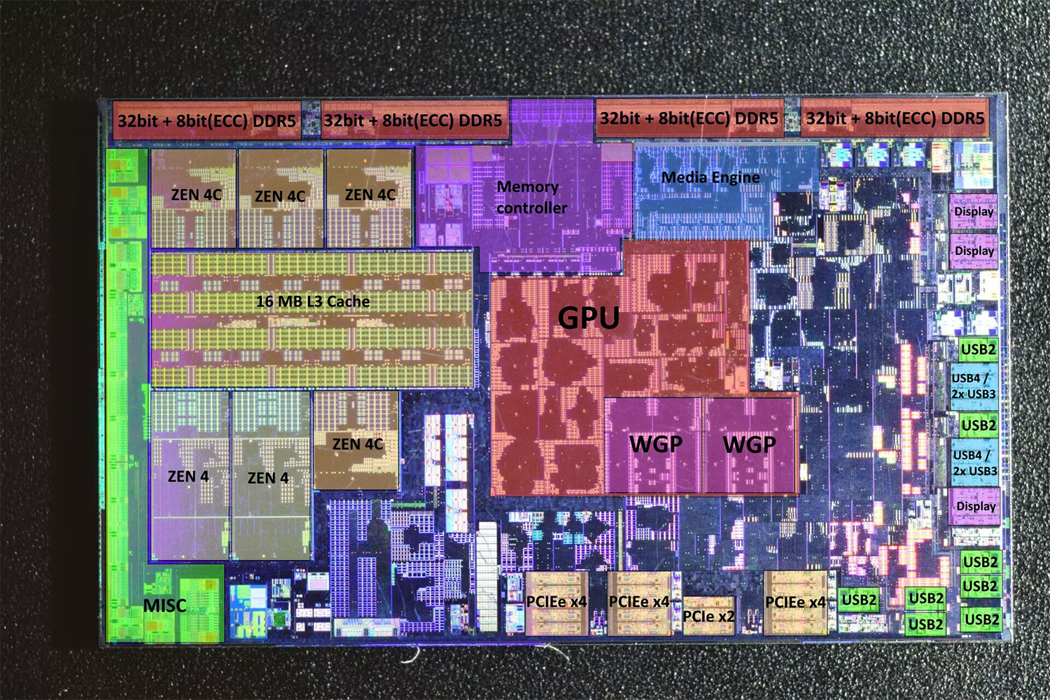
AMD did not release any first-party die shots, renders, or block-diagrams of the Phoenix 2 silicon, but here is a public annotation of the die by BusAlexey on X, which is based on a public die-shot.

AMD Ryzen 5 8500G is based on the 4 nm Phoenix 2 silicon, which is physically smaller than the 4 nm Phoenix silicon driving the Ryzen 5 8600G and Ryzen 7 8700G. This chip comes with a die area of 137 mm², compared to the 178 mm² of Phoenix. AMD was able to make the chip smaller by limiting the CPU to just 6 cores, four of which are the 35% smaller Zen 4c cores, truncating the iGPU to just 4 CU (256 stream processors), removing the XDNA NPU, and reducing the PCI-Express root complex to just 14 Gen 4 lanes, compared to the 20 Gen 4 lanes on Phoenix.
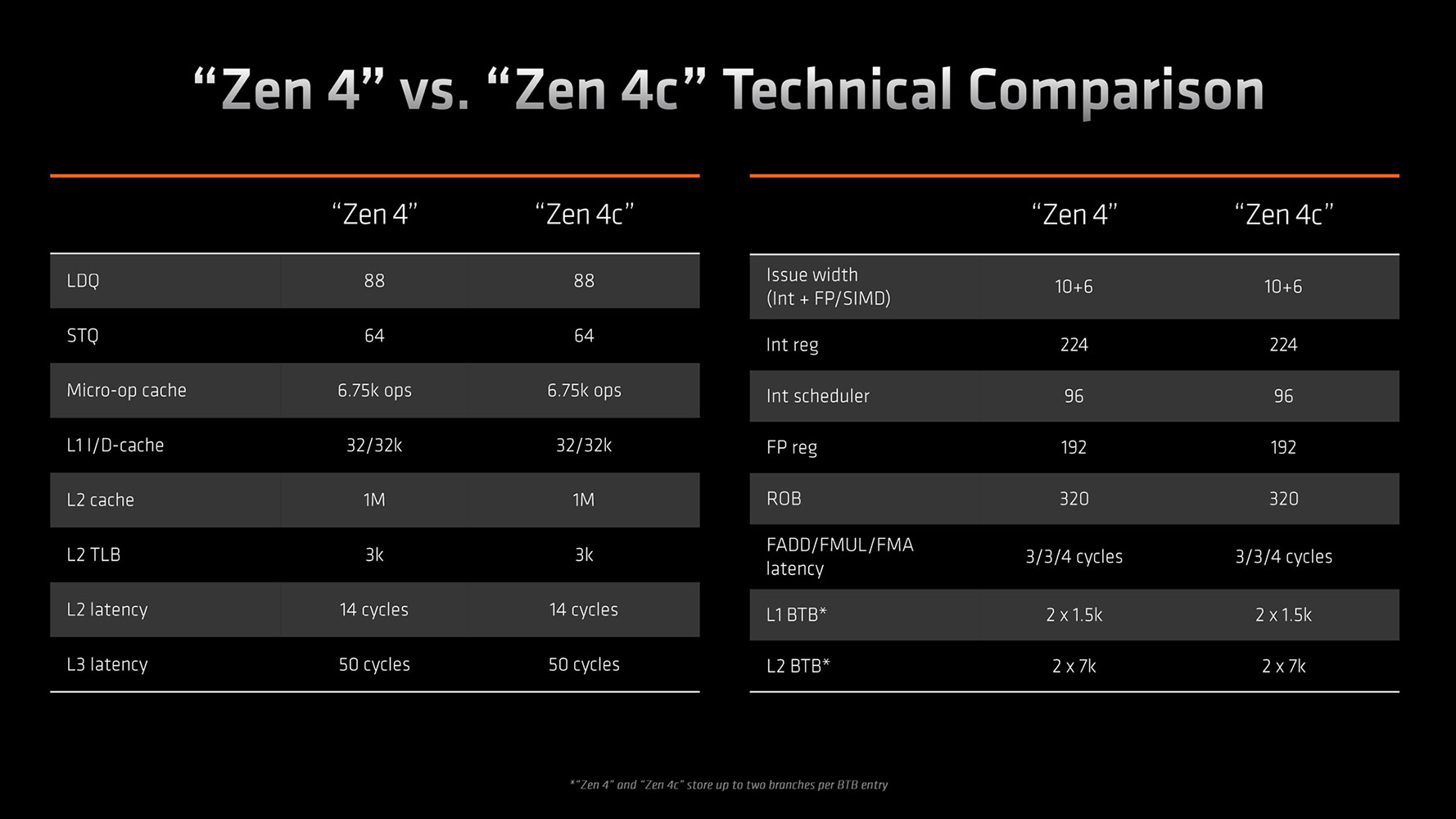
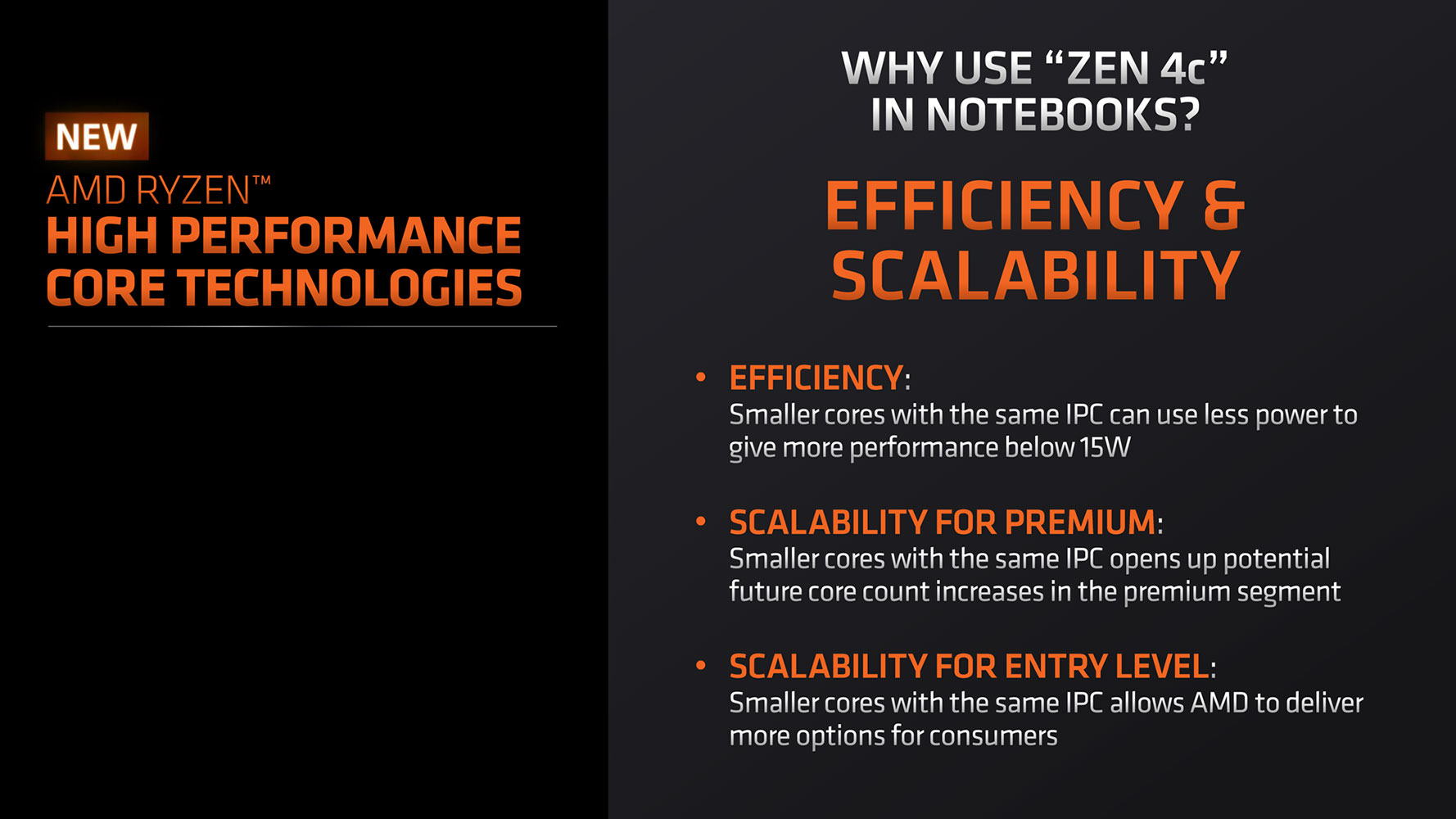
The Zen 4c core is a spatially compacted version of Zen 4. No components are removed, and nothing is truncated. Even the L1 and L2 caches remain the same. What's changed is that AMD has used higher density libraries, and compacted the components at a silicon level. The resulting core offers the same exact IPC as Zen 4, it also supports SMT (two threads per core), and has an identical ISA (instruction sets), which means threads can seamlessly migrate between Zen 4 and Zen 4c cores without an ISA mismatch causing runtime errors.
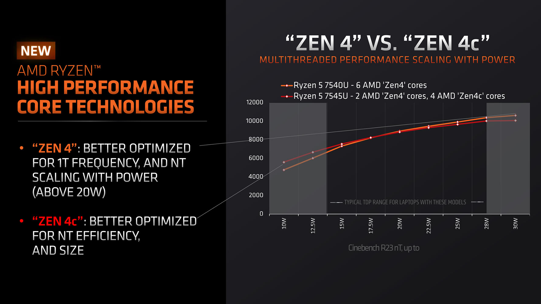
The only trade-off with the Zen 4c engineering effort is performance (not IPC). Zen 4c has much lower voltage limits than Zen 4, which means it has a narrower clock speed band, and so any threads migrating from a Zen 4 core to a Zen 4c core will only experience lower performance, but not the lack of any hardware features. This common IPC and ISA means that the Zen 4 and Zen 4c cores sit in a common core complex (CCX), and share a 16 MB L3 cache, which should greatly benefit thread migration between the two core types.
AMD's approach to heterogeneous multicore is significantly different from that of Intel's. Because the P-core and E-core are significantly different to each other, with different IPC and ISA, Intel relies on a hardware scheduler called Thread Director, which ensures that the right kind of workload is allocated to the right core type. This is not the case with Phoenix 2. AMD is using UEFI CPPC preferred cores mechanism to mark the two Zen 4 cores as preferred cores to the OS, which ensures that most of the workload is sent to them, as they support the highest boost frequencies. Spillover workloads are allocated to the Zen 4c cores.
The platform I/O of the Phoenix 2 silicon is severely truncated from the regular Phoenix silicon powering the 8600G and 8700G. Its PCI-Express interface is limited to 14 lanes of PCI-Express 4.0, compared to the 20 lanes on Phoenix, and the lavish 28 Gen 5 lanes on the Raphael MCM. Socket AM5 motherboards handle the I/O of Phoenix 2 by wiring out just four Gen 4 lanes to the PCI-Express x16 PEG slot (now electrical PCI-Express 4.0 x4), and connecting just one of the two CPU-attached M.2 NVMe slots, which operates at Gen 4 x4. The chipset bus takes away another 4 lanes, leaving 2 lanes that are configurable as 20 Gbps USB 3.2, or to drive other onboard devices. The memory I/O is unchanged, you get two channels of DDR5.
The iGPU of Phoenix 2 is based on the latest RDNA 3 graphics architecture, and uses the latest versions of the Video CoreNext (VCN) media acceleration, as well as the latest Display CoreNext (DCN); but with just two workgroup processors (WGPs), or just 4 CUs, which work out to 256 stream processors, with 8 ROPs. The GPU ticks at 2.80 GHz. AMD has branded this iGPU the Radeon 740M. While it's still not the best fit for any gaming at 1080p, it should play some casual games at 720p, and you should get a fairly decent non-gaming experience, such as rich web rendering or high-resolution video. This should be sufficiently powerful as a HTPC iGPU, provided your motherboard has the right display connectors. The iGPU can decode H.265 4K video at 175 FPS. So there's plenty of heft for a 4K media experience.
The Zen 4 Microarchitecture
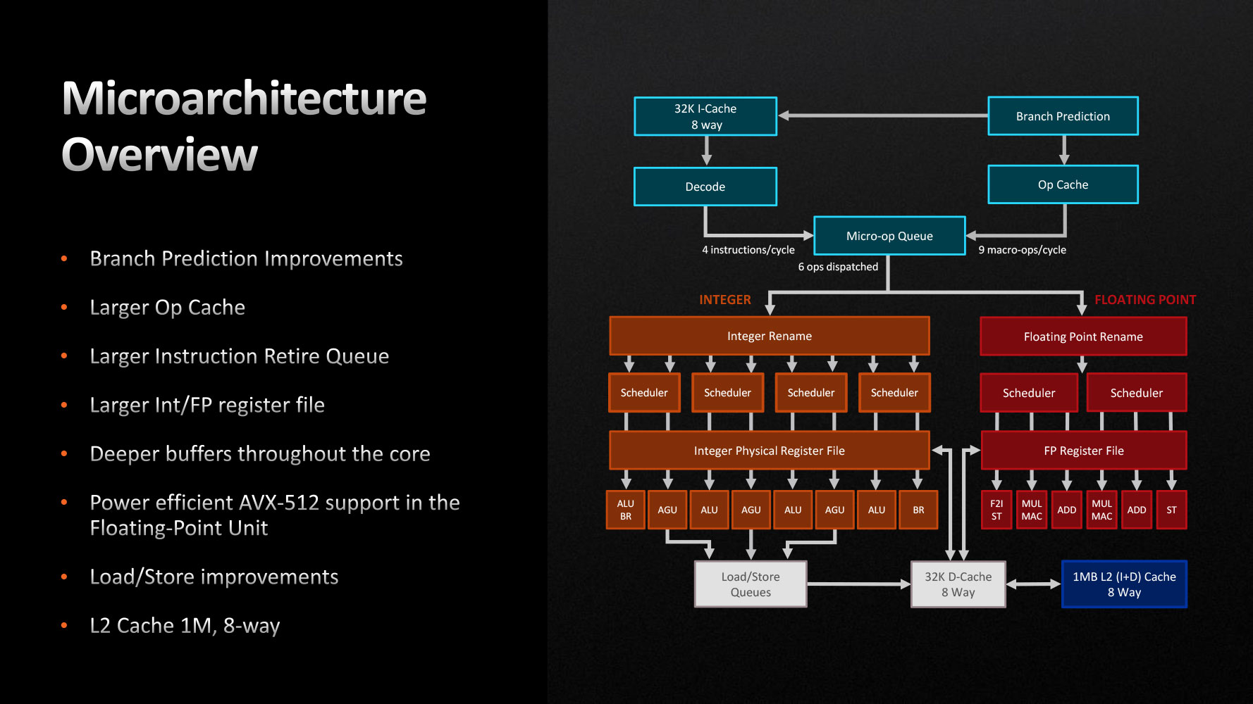
All cores in Ryzen 7000 series processors are of the same kind, what Intel would consider a performance-core, or P-core. AMD has worked on all three key stages of the CPU—the front-end, the execution, and the load/store. The front-end is the "mouth" of the CPU core, and prepares data and instructions for execution. Front-end improvements begin at the Branch Prediction unit, which can now predict 2 taken branches per clock-cycle, and comes with larger L1 and L2 branch-target buffers (BTBs). AMD had for the very first time introduced an op cache with Zen, improving it over time. AMD has increased the size of the op cache by around 68 percent. It can now handle 9 macro-ops per cycle. The micro-op queue dispatch rate to the execution stage is still 6.
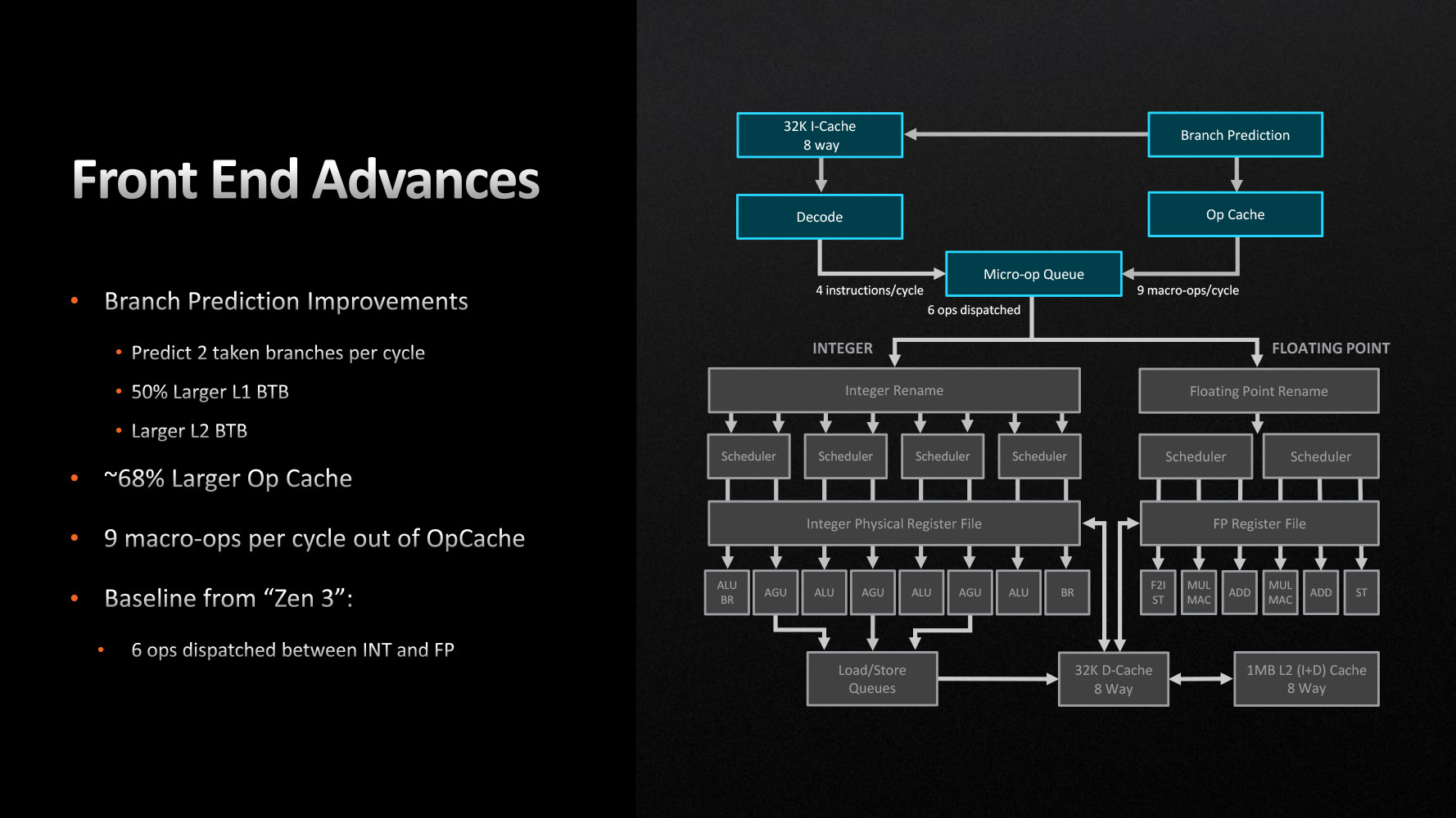
The Execution Stage is the main number-crunching machinery, and broadly features two components for the kind of math workload being executed—Integer and Floating Point. The "Zen 4" execution stage features a 25% larger instruction retire queue, larger register files, and higher buffer queue-depths throughout the core.
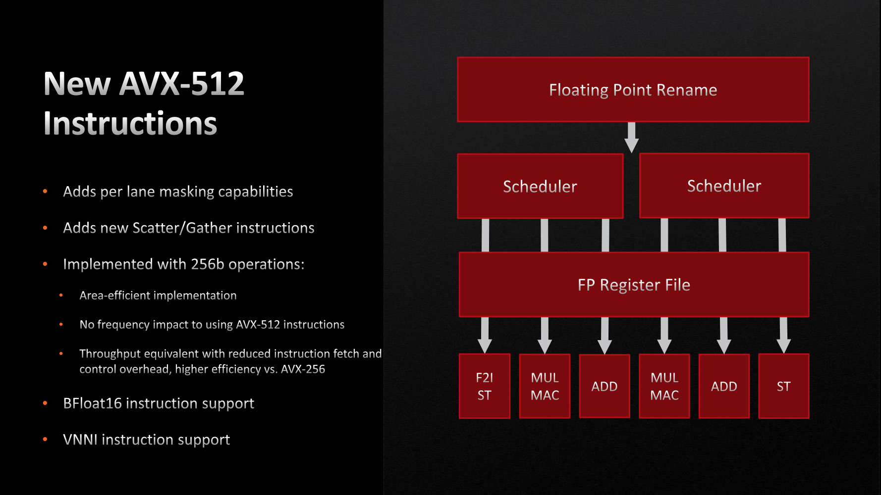
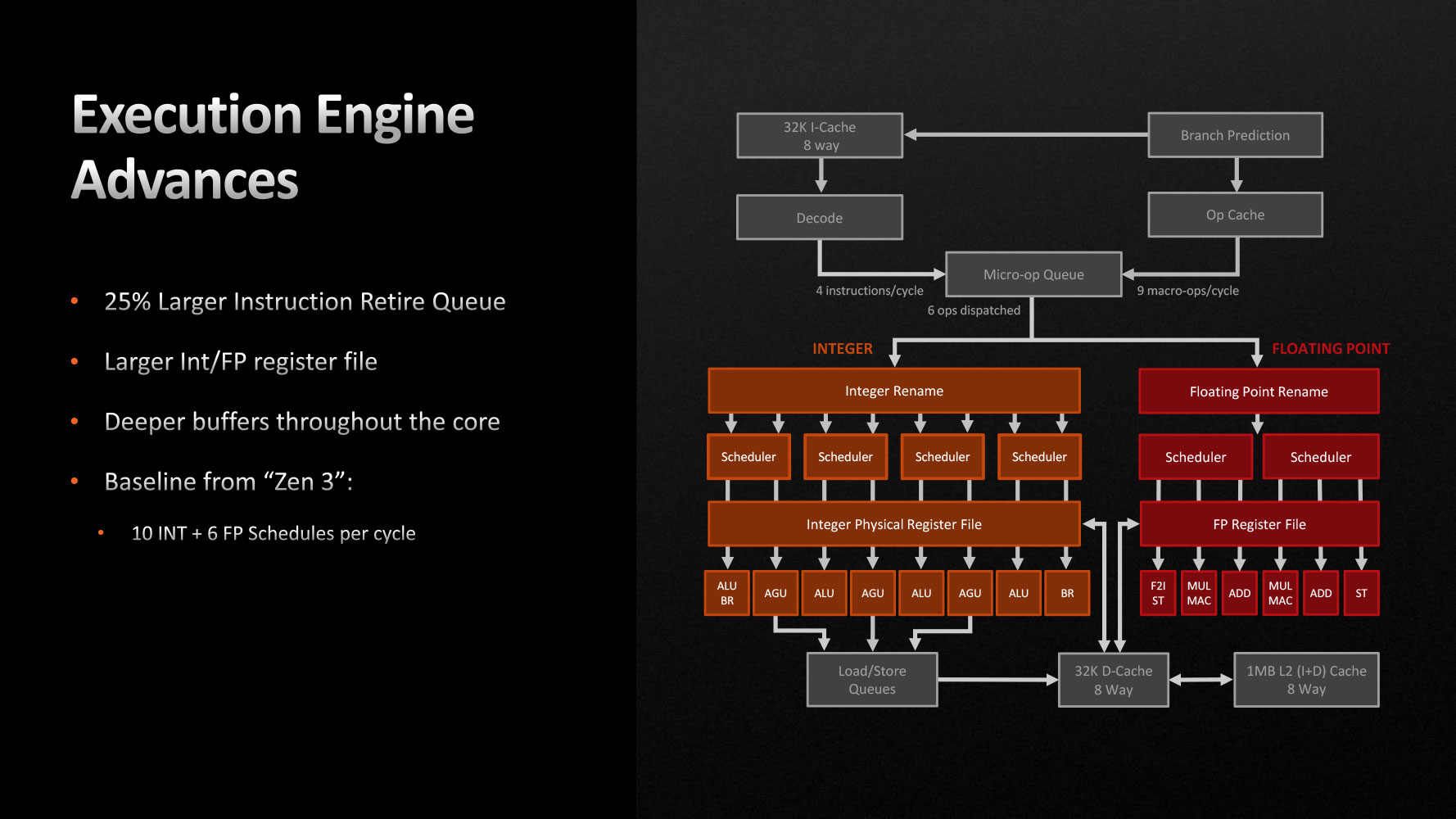
With "Zen 4," AMD is introducing support for AVX-512, in a bid to increase the processor's AI inferencing performance. The company did this in a die-area efficient, and energy-efficient manner, with no impact on CPU core frequency. AVX-512 operations are executed on a dual-pumped 256-bit FPU, rather than building ground-up 512-bit FP machinery. VNNI and Bfloat16 instruction-sets are also added, which mean that "Zen 4" can handle pretty much all of the AVX-512 client-relevant workloads that competing Intel processors can.
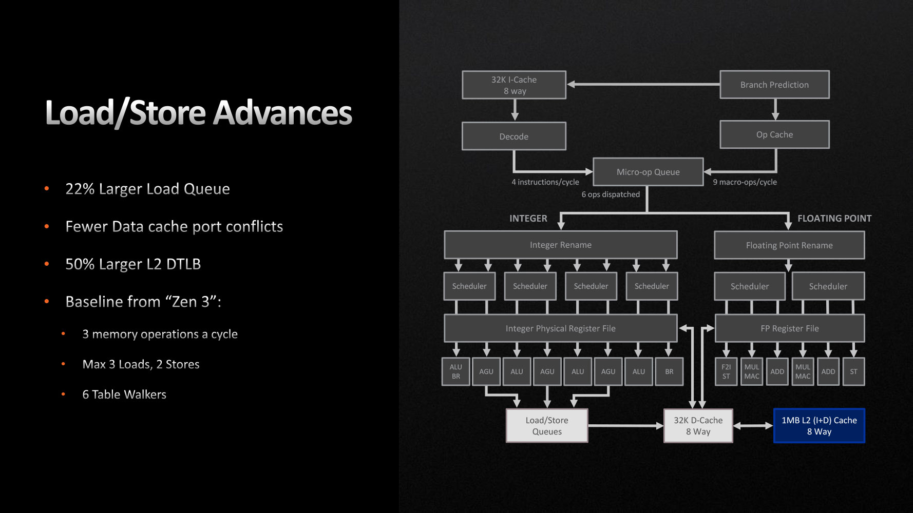
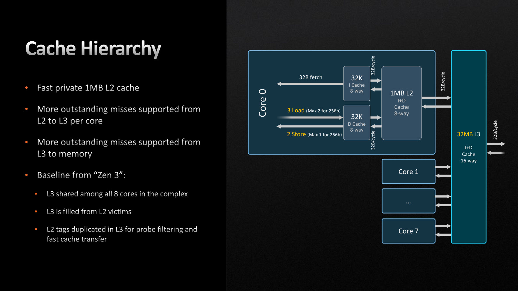
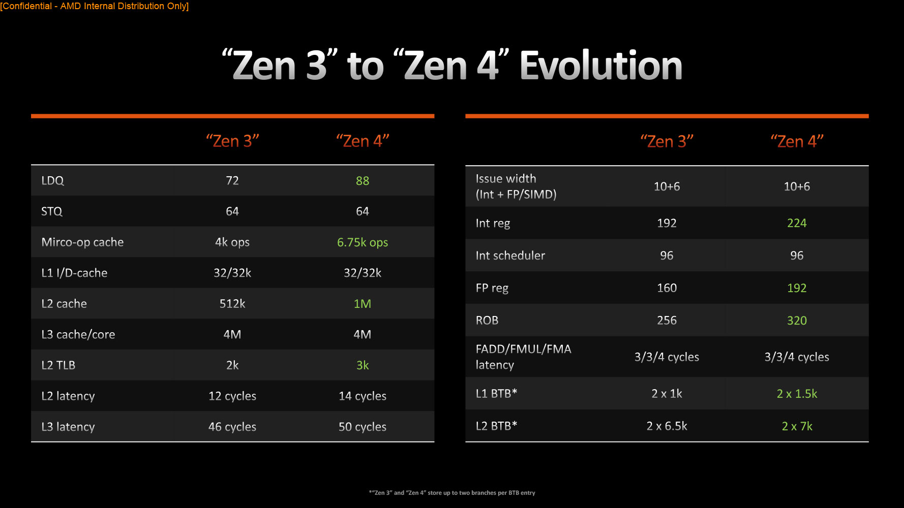
The Load/Store unit is the part of the core that interfaces with the memory sub-system. The "Zen 4" core gets a 22 percent larger Load Queue, with improved data-port conflict-resolution. There's a 50% larger L2 data transition lookaside buffer. The cache-hierarchy of the Ryzen 7000 desktop processor is similar to that of Ryzen 5000, with a few key differences, besides bandwidth/latency improvements—the dedicated L2 cache has been doubled in size to 1 MB per core. The eight CPU cores on a CCD share a monolithic 32 MB L3 cache, with uniform access to each core.
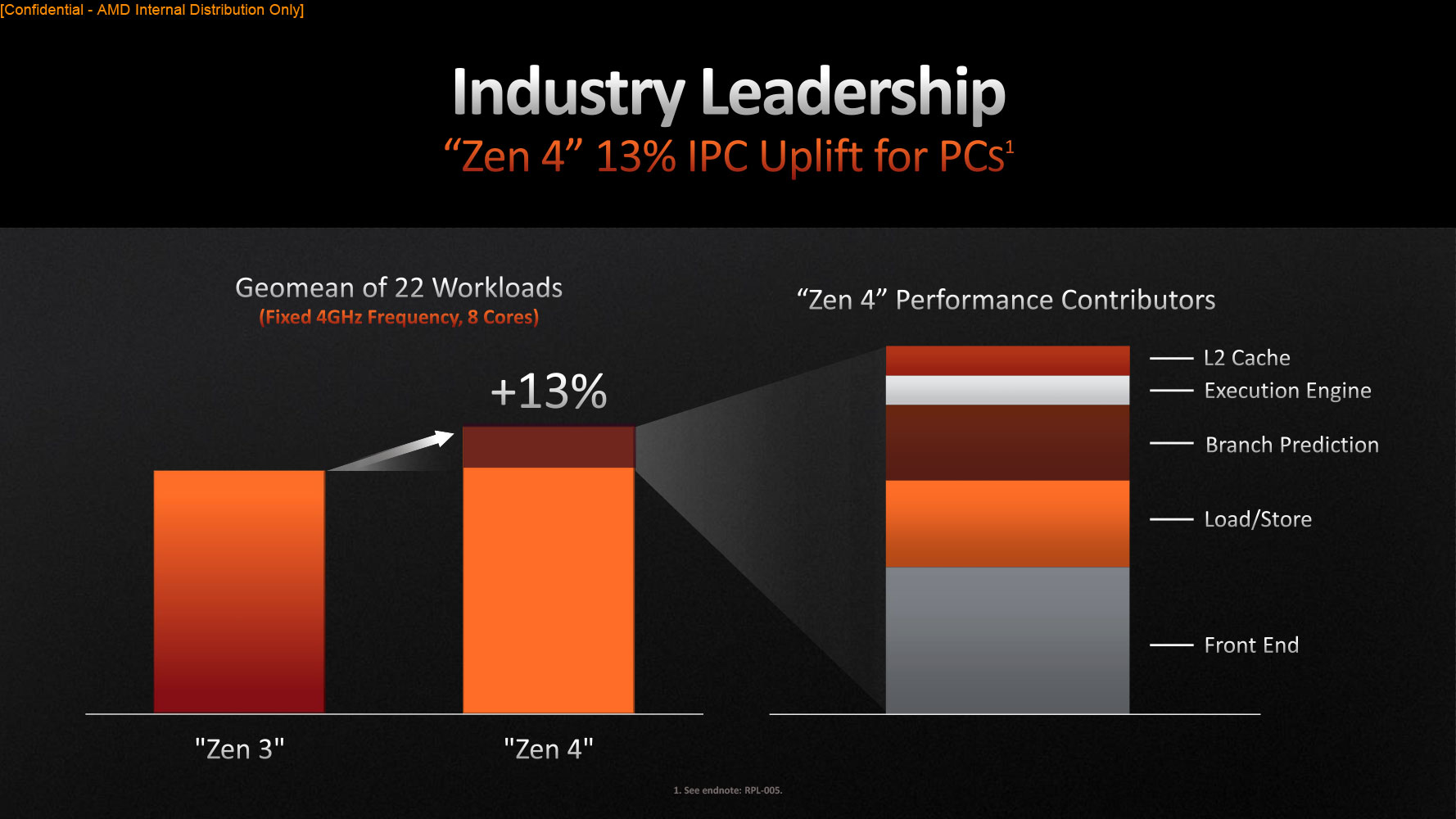
These improvements contribute to a 13 percent IPC improvement over "Zen 3," AMD claims. The company provided a break-up of which components are contributing to the IPC uplift, and we see that close to two-thirds of it are coming from improvements to the front-end and load/store stages. Branch prediction improvements contribute a fifth of this uplift. Interestingly, the L2 cache contributes barely 1/10th of the IPC uplift, in the tested applications—we believe this increase is mostly relevant for server workloads where it should be able to make a difference. Intel's "Golden Cove" P-core comes with 1.25 MB L2 cache, and "Raptor Cove" features 2 MB. Despite the doubling in L2 cache sizes, the resulting increase in cache latency is very well contained (from 12 cycles on the 512 KB L2 of "Zen 3," to just 14 cycles on "Zen 4").
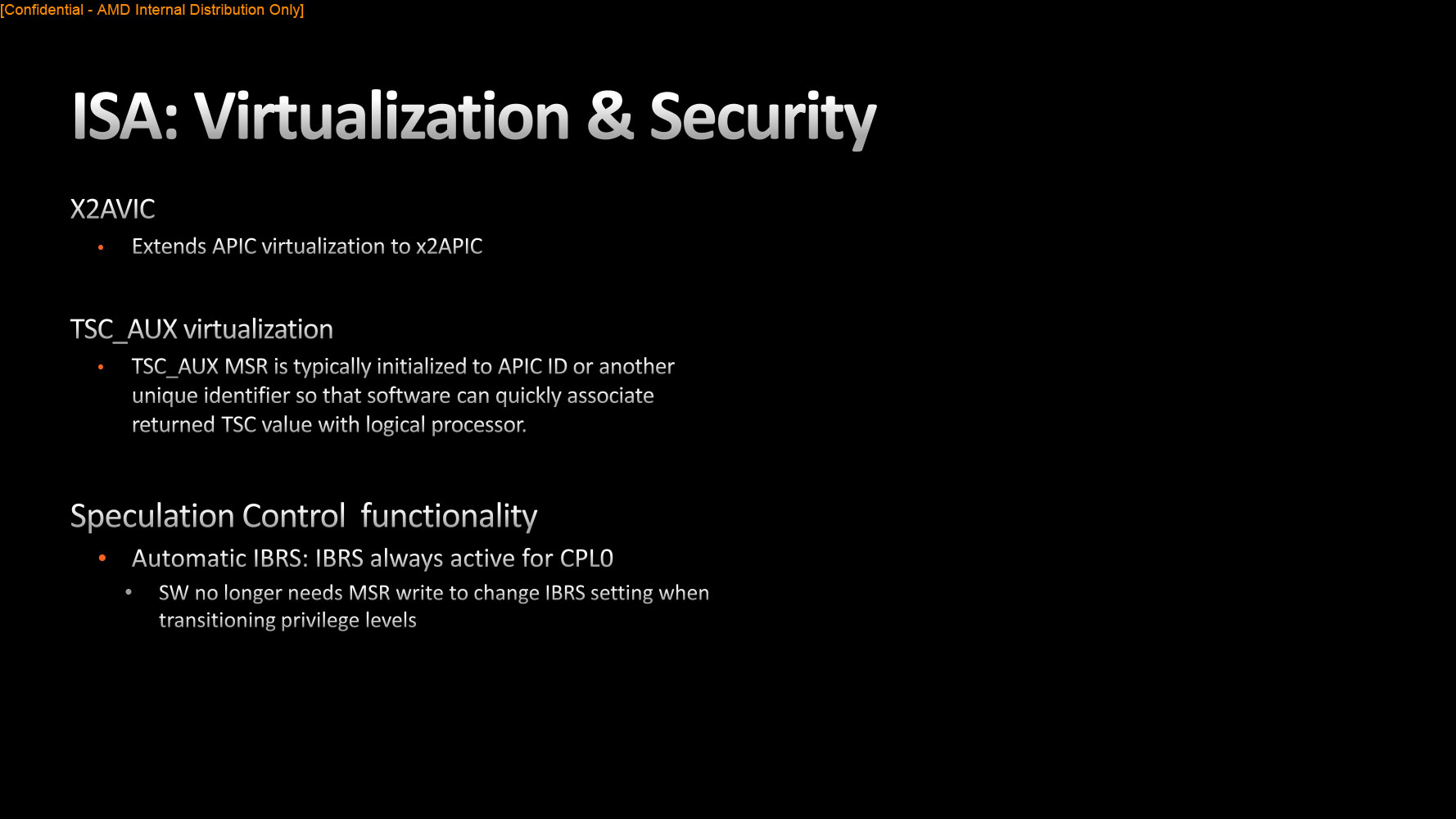
VBS (virtualization-based security) is the standard on new Windows 11 installs and gets activated automatically, unless you specifically disable it. Windows 11 Security Center already flags VBS not being enabled as a warning, similar to the Antivirus being disabled or outdated. AMD made several improvements to the Virtualization feature-set, to reduce its performance impact in a VBS-enabled client environment. This includes speculation control, dual AVIC to go with the physical dual-APIC, and TSC_AUX virtualization.
Jun 30th, 2025 22:41 CDT
change timezone
Latest GPU Drivers
New Forum Posts
- GravityMark v1.89 GPU Benchmark (303)
- Post your Cinebench 2024 score (658)
- GPU PerfCap Reason PWR (8)
- Laptop overclocking adventures (1238)
- [INTEL]-How To Update Your Microcode for Intel HX 13/14th Gen. CPUs Laptops/Mobile Easily. (172)
- Will you buy a RTX 5090? (584)
- The TPU UK Clubhouse (26530)
- Optane and "enable write caching " (27)
- Question about Intel Optane SSDs (87)
- Do you use Linux? (664)
Popular Reviews
- ASUS ROG Crosshair X870E Extreme Review
- Sapphire Radeon RX 9060 XT Pulse OC 16 GB Review - Samsung Memory Tested
- AVerMedia CamStream 4K Review
- Lexar NQ780 4 TB Review
- AMD Ryzen 7 9800X3D Review - The Best Gaming Processor
- Upcoming Hardware Launches 2025 (Updated May 2025)
- Sapphire Radeon RX 9070 XT Nitro+ Review - Beating NVIDIA
- AMD Ryzen 9 9950X3D Review - Great for Gaming and Productivity
- NVIDIA GeForce RTX 5060 8 GB Review
- ASRock Phantom Gaming Z890 Riptide Wi-Fi Review
TPU on YouTube
Controversial News Posts
- Intel's Core Ultra 7 265K and 265KF CPUs Dip Below $250 (288)
- NVIDIA Grabs Market Share, AMD Loses Ground, and Intel Disappears in Latest dGPU Update (204)
- Some Intel Nova Lake CPUs Rumored to Challenge AMD's 3D V-Cache in Desktop Gaming (140)
- NVIDIA Launches GeForce RTX 5050 for Desktops and Laptops, Starts at $249 (105)
- Microsoft Partners with AMD for Next-gen Xbox Hardware (105)
- Intel "Nova Lake‑S" Series: Seven SKUs, Up to 52 Cores and 150 W TDP (100)
- NVIDIA GeForce RTX 5080 SUPER Could Feature 24 GB Memory, Increased Power Limits (94)
- Reviewers Bemused by Restrictive Sampling of RX 9060 XT 8 GB Cards (88)