 53
53
AMD Ryzen 7 3800XT Review
(53 Comments) »Introduction
It's been exactly a year since AMD debuted the Ryzen 3000 "Zen 2" processors, and the company hence decided to refresh their lineup with three new product additions as part of the Ryzen 3000 "XT" series. The company's "Zen 3" architecture will be out later this year, probably near the end of it, and AMD is facing competition from the recently launched 10th Gen Core "Comet Lake" processor family by Intel. Still, the Ryzen 3000 desktop processor family is one of many firsts for AMD, including first to market with 7 nm and PCI-Express gen 4.0, and it is the first core IPC parity with Intel in over 15 years.
AMD's third-generation Ryzen has had a free reign over the market until Intel launched its 10th Gen Core desktop processor family. In the past, AMD based its competitiveness on offering more cores/threads to the dollar. Intel's 9th generation chips still had a slight edge with gaming performance on account of higher clock speeds. With "Comet Lake," Intel decided to unleash the "Skylake" microarchitecture by enabling HyperThreading across the board, increasing clock speeds, introducing new boosting algorithms for its Core i7 and Core i9 processor families, and greatly relaxing power limits for these chips, including giving motherboard designers the freedom to tweak power and thermal values better. These helped Intel restore performance parity with AMD across segments, while increasing its edge in gaming performance.
Intel's heavily marketed performance leadership, particularly in gaming performance, rest on just single-digit percentages, which AMD feels it can easily narrow with its existing "Zen 2" IP, without having to cede the market to Intel for the next few months until "Zen 3" relieves the product stack. This is the sole design goal of the Ryzen 3000XT product family.

Our Ryzen 7 3800XT review takes a look at this 8-core/16-thread processor being launched today at $399—the launch price of the 3800X. The Core i7-10700K has largely eroded the performance leadership of the 3800X, forcing AMD to sell it at prices under $340. The 3800XT is then an attempt by AMD to sell an 8-core part at $399 again. It comes with increased frequencies, featuring the same 3.90 GHz nominal clocks as the 3800X, but maximum boost frequency that have been increased by 200 MHz—now at 4.70 GHz compared to the 4.50 GHz of the 3800X and 4.40 GHz of the 3700X. There is more to the Ryzen 3000XT series than just speed bumps, as we'll explain on the Architecture page.
An interesting product design decision by AMD has been to exclude the box cooler with the Ryzen 3800XT—something that's included on the 3800X and even the 3900X. In their briefings, AMD explained that the target audience of the 3800XT will be using the chip with aftermarket cooling solutions anyway, although we believe the motive to be cost-cutting (a straight $25–$30 saving with no Wraith Prism RGB cooler included). Skipping the cooler puts the onus of having good enough cooling for the processor to hit the maximum boost and overclock well on the user.
In this Ryzen 7 3800XT review, we'll compare it with its "predecessors" and the Intel Core i7-10700K across our entire selection of CPU and gaming benchmarks to see if AMD deserves to sell the processor at its price.
| Price | Cores / Threads | Base Clock | Max. Boost | L3 Cache | TDP | Architecture | Process | Socket | |
|---|---|---|---|---|---|---|---|---|---|
| Ryzen 5 3600X | $205 | 6 / 12 | 3.8 GHz | 4.4 GHz | 32 MB | 95 W | Zen 2 | 7 nm | AM4 |
| Ryzen 5 3600XT | $250 | 6 / 12 | 3.8 GHz | 4.5 GHz | 32 MB | 95 W | Zen 2 | 7 nm | AM4 |
| Ryzen 7 1800X | $250 | 8 / 16 | 3.6 GHz | 4.0 GHz | 16 MB | 95 W | Zen | 14 nm | AM4 |
| Core i7-8700K | $350 | 6 / 12 | 3.7 GHz | 4.7 GHz | 12 MB | 95 W | Coffee Lake | 14 nm | LGA 1151 |
| Core i7-9700K | $380 | 8 / 8 | 3.6 GHz | 4.9 GHz | 12 MB | 95 W | Coffee Lake | 14 nm | LGA 1151 |
| Core i7-10700K | $375 | 8 / 16 | 3.8 GHz | 5.1 GHz | 16 MB | 125 W | Comet Lake | 14 nm | LGA 1200 |
| Ryzen 7 3700X | $275 | 8 / 16 | 3.6 GHz | 4.4 GHz | 32 MB | 65 W | Zen 2 | 7 nm | AM4 |
| Ryzen 7 3800X | $340 | 8 / 16 | 3.9 GHz | 4.5 GHz | 32 MB | 105 W | Zen 2 | 7 nm | AM4 |
| Ryzen 7 3800XT | $400 | 8 / 16 | 3.9 GHz | 4.7 GHz | 32 MB | 105 W | Zen 2 | 7 nm | AM4 |
| Ryzen 9 3900X | $430 | 12 / 24 | 3.8 GHz | 4.6 GHz | 64 MB | 105 W | Zen 2 | 7 nm | AM4 |
| Ryzen 9 3900XT | $500 | 12 / 24 | 3.8 GHz | 4.7 GHz | 64 MB | 105 W | Zen 2 | 7 nm | AM4 |
| Core i9-9900K | $530 | 8 / 16 | 3.6 GHz | 5.0 GHz | 16 MB | 95 W | Coffee Lake | 14 nm | LGA 1151 |
| Core i9-9900KS | $600 | 8 / 16 | 4.0 GHz | 5.0 GHz | 16 MB | 127 W | Coffee Lake | 14 nm | LGA 1151 |
| Core i9-10900K | $500 | 10 / 20 | 3.7 GHz | 5.3 GHz | 20 MB | 125 W | Comet Lake | 14 nm | LGA 1200 |
A Closer Look


The Ryzen 7 3800XT ships in a paperboard box with a cutout showing the processor inside. The box does not include a cooler.


The processor looks like any conventional AMD CPU, with a large IHS dominating the top and a 1,331-pin micro-PGA in the bottom. The "Zen 2" CCD chiplet is made in Taiwan and the I/O die in the US, and the two are put together at a facility in China.
All Ryzen 3000XT series processors are designed to be drop-in compatible with any Socket AM4 motherboard that supports Ryzen 3000 processors.

The Ryzen 7 3800XT can be paired with a fairly big selection of AM4-compatible coolers that have been released since 2017.
Architecture
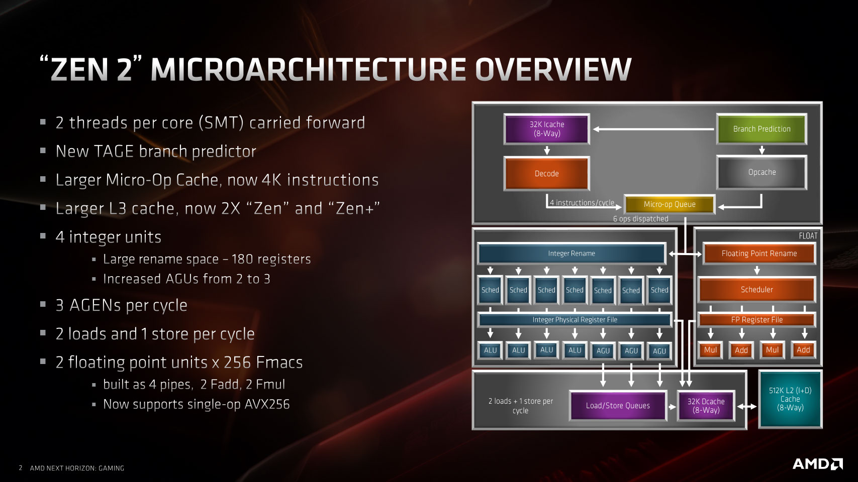
The architecture is no different from the Ryzen 9 3950X or any other "Matisse," so you can click on the button below to read about it, or skip that section if you're familiar with it.
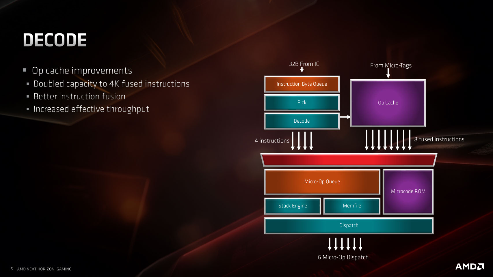


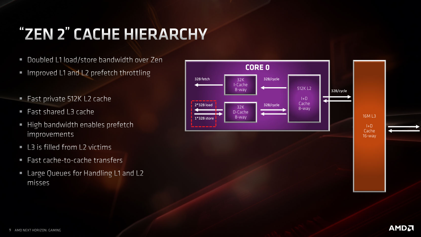

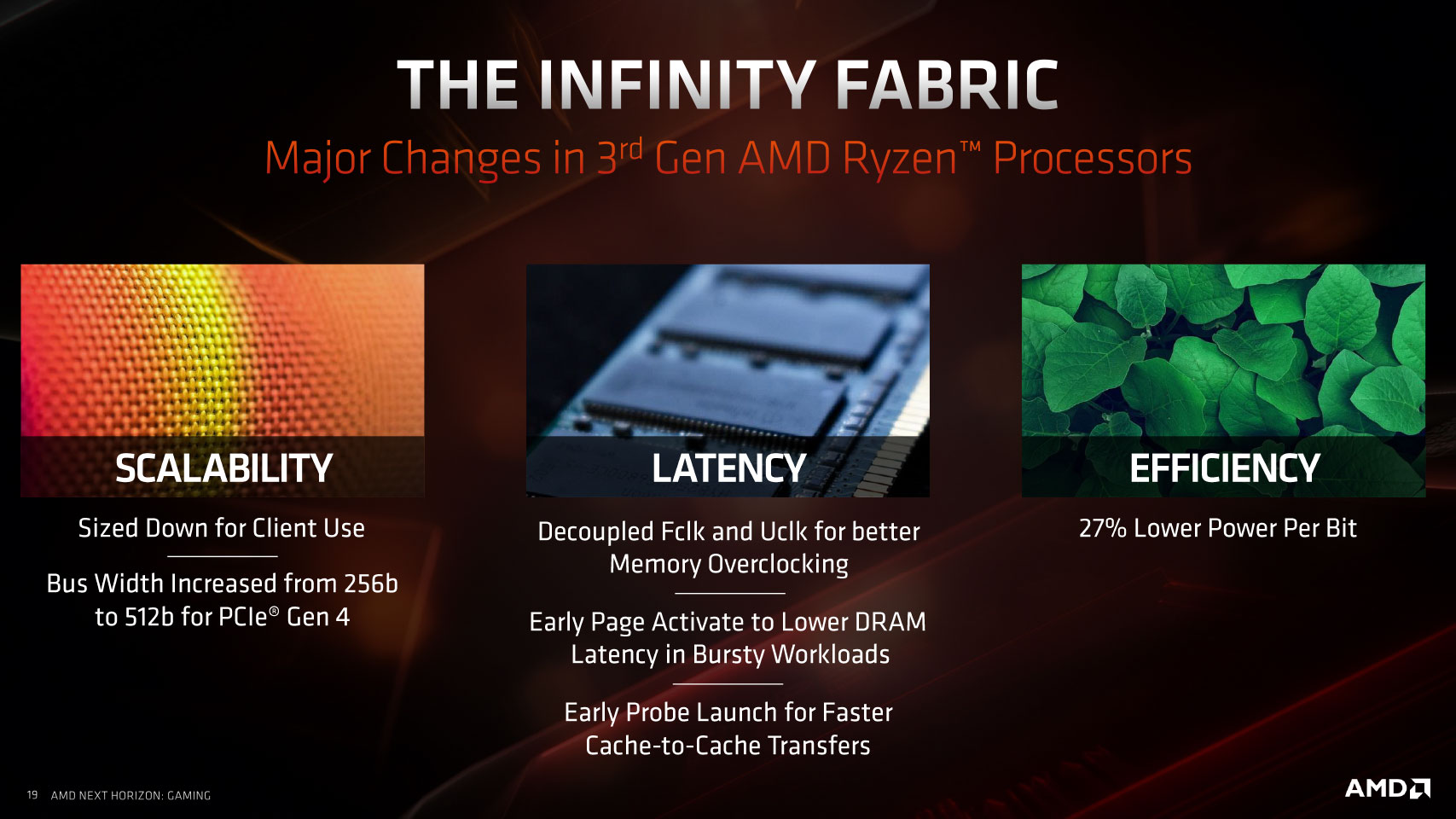
Architectural Innovations Specific to Ryzen 3000XT Series
AMD internally refers to the Ryzen 3000XT family of processors as "Matisse 2." These are almost identical to the original Ryzen 3000 "Matisse" processors based on the "Zen 2" microarchitecture, but AMD has given these processors some physical improvements. To begin with, the 8-core CCDs (compute complex dies) or "Zen 2" chiplets inside the processors are still based on TSMC N7 (the foundry's first 7 nm node), but with certain refinements. AMD claims these yields a single-digit percentage electrical improvement, which AMD uses to achieve up to 200 MHz increments in maximum boost frequencies without it affecting the TDP of these processors.
The TDP of Ryzen 5 3600XT remains at 95 W, just like the 3600X, while both the 3800XT and 3900XT stick with 105 W TDP. AMD's decision not to include cooling solutions with the 3800XT and 3900XT have little to do with the power or thermals of these processors and more with marketing decisions taken by AMD. It certainly reduces AMD's bill of materials for these chips.
AMD categorically stated that this "refined" N7 node is neither N7P nor N7+. The N7P node is the successor to N7 that sticks to DUV (deep ultraviolet) lithography, but innovates in certain other areas to eke out a power improvement. N7+, on the other hand, uses EUV (extreme ultraviolet) lithography that not only yields much higher efficiency, but also over a 20% increase in transistor-density. The node AMD is building "Matisse 2" on is still N7, but with certain refinements AMD didn't elaborate in its product brief.
AMD B550 and X570 Chipsets
With premium AMD X570 chipset-based motherboards starting at $150, it's less likely that someone would pair the third-generation Ryzen 3 with it. Choosing a cheaper B450 motherboard would mean giving up on killer features such as PCIe gen 4.0. AMD hence launched the new B550 mid-range chipset alongside these processors. The B550 chipset lets you have PCI-Express gen 4.0 connectivity from the "Matisse" processor, while limiting general-purpose PCIe downstream connectivity to gen 3.0.
On a typical B550 chipset motherboard, the main PCI-Express x16 slot will be gen 4.0 if paired with a third-generation Ryzen "Matisse" processor, as would one of the board's M.2 NVMe slots that's wired to the processor. All other PCIe or M.2 slots which are wired to the B550 chipset will be gen 3.0. This way, future-proofing of the platform for next-generation graphics cards and SSDs remains intact. The B550 chipset provides up to six SATA 6 Gbps ports with AHCI and RAID capability, up to two 10 Gbps USB 3.1 gen 2 ports (in addition to four such ports put out by the "Matisse" processor), two additional USB 3.1 gen 1 ports, and six USB 2.0 ports. The platform's HDA and LPCIO buses are located on the processor.
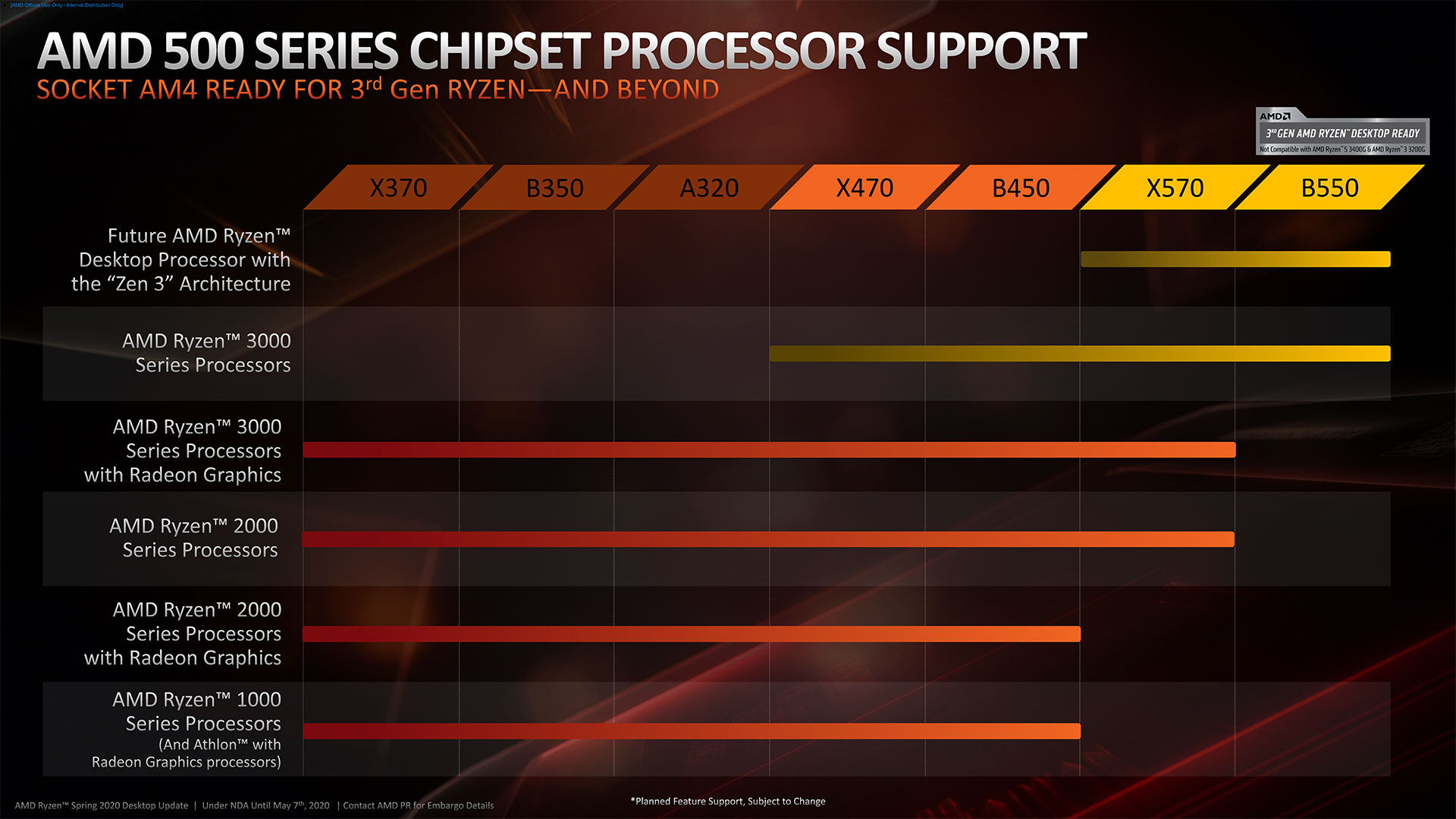
A word on compatibility. The B550 chipset only supports third-generation Ryzen "Matisse" processors as of this writing, and AMD confirmed support for next-generation processors based on the "Zen 3" architecture. You cannot pair a B550 motherboard with older Ryzen 2000/1000 processors or even the 3200G or 3400G APUs based on the older "Zen+" microarchitecture. There will be clear labeling on B550 chipset motherboard boxes to this effect.
What we like most about the B550 is its low TDP, which lets motherboard designers make do with passive heatsinks; unlike X570, which requires active fan heatsinks.
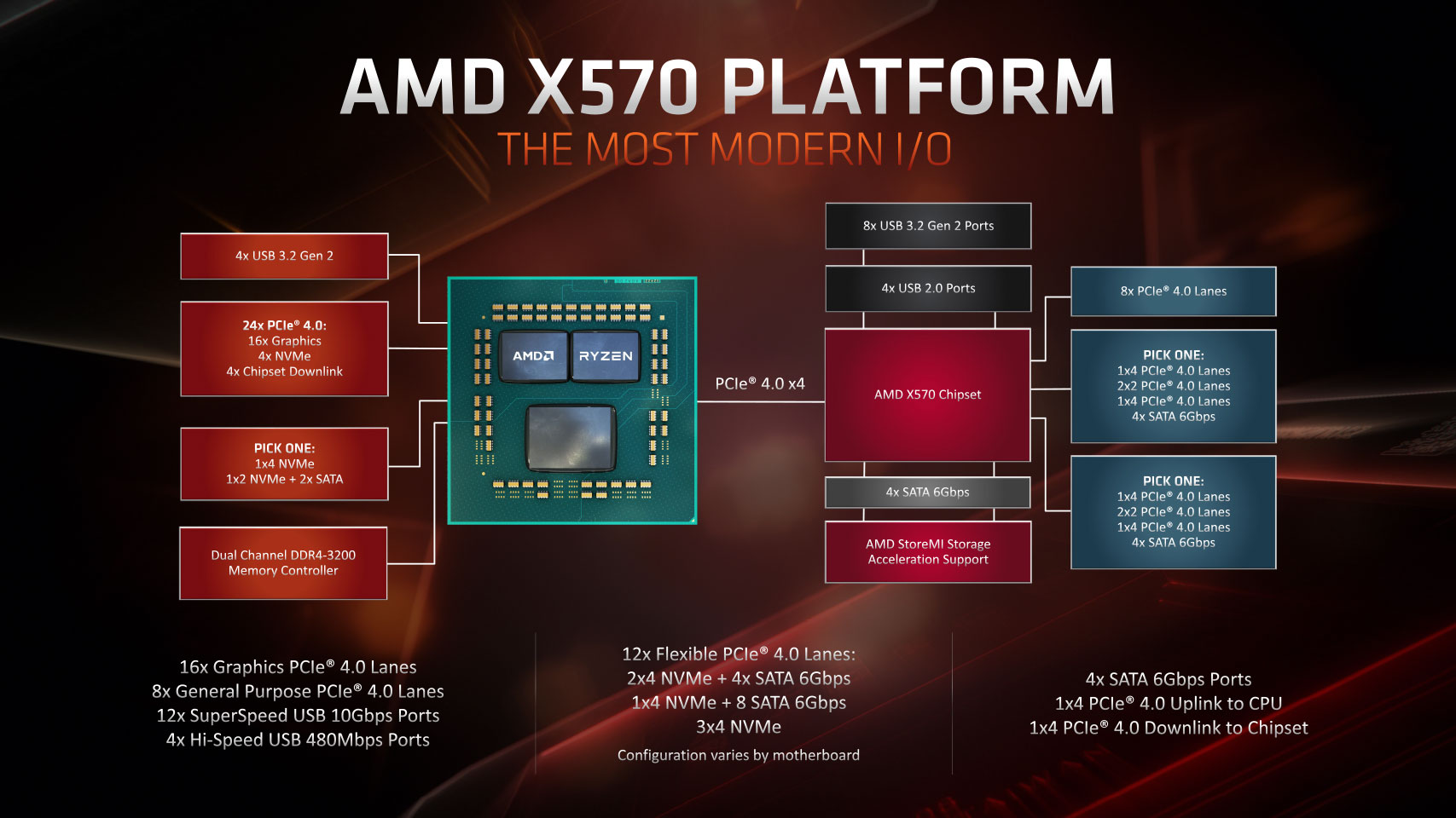
AMD delivered on its promise of third-generation Ryzen "Matisse" processors being backwards compatible with older Socket AM4 motherboards, going all the way back to the AMD 300-series chipset, with a simple BIOS update. To make the most out of Ryzen "Matisse"—namely, PCI-Express gen 4.0 connectivity and increased CPU/memory overclocking headroom, you're expected to use one of the latest motherboards that use the AMD X570 chipset. The X570 is an entirely different chip from X470 and X370. The older chipsets were supplied by ASMedia and were rather slim in their downstream connectivity.
The X470 only puts out 8 PCIe gen 2.0 downstream lanes, for example. The X570 modernizes all I/O by putting out up to 16 PCIe gen 4.0 downstream lanes. This enables additional M.2 PCIe gen 4 slots on your motherboards for the latest SSDs featuring PCIe gen 4 support and creates room for many new bandwidth-hungry onboard devices, such as 10 GbE adapters, next-generation Thunderbolt, 802.11ax controllers, etc. Along with the "Matisse" SoC, the X570 also puts out a number of 10 Gbps USB 3.1 gen 2 ports. Motherboards based on X570 also implement modern network connectivity options, such as 2.5 GbE and 802.11ax WLAN.
Given there are highly capable motherboards based on the B550 chipset with serious VRM solutions and high-end connectivity, it's good enough for any Ryzen 3000XT series processor, including the 3900XT. The B550 chipset also offers multi-GPU support. Your choice between the B550 and X570 should hence boil down to whether you plan to have more than one M.2 NVMe SSD that can take advantage of PCI-Express gen 4.0, or an NVMe RAID setup of 2–3 PCIe gen 4.0-capable M.2 SSDs. Serious overclockers should still consider the X570 since the most beastly VRM setups are still found on boards such as the MSI MEG X570 GODLIKE, ASUS ROG Crosshair VII Formula, and GIGABYTE X570 AORUS Xtreme.
Our Patreon Silver Supporters can read articles in single-page format.
Apr 9th, 2025 03:31 EDT
change timezone
Latest GPU Drivers
New Forum Posts
- 9070XT or 7900XT or 7900XTX (165)
- (Some of) What I'd like to See From a Final Fantasy IX Remake (3)
- ThrottleStop - 14900HX, 4090RTX MSI laptop (9)
- V/F Points not being respected consistantly (3)
- "The system hibernated due to a critical thermal event" - at 54c?! (2)
- Post your cooling. (209)
- PSA: if your 5070 Ti freezes up (even the mouse cursor won't move) with Furmark. Try turning off Gsync to fix it! (1)
- issue with restart after changing throttlestop settings (5)
- Stock PSU with Razer Core X with adapter to 12VHPWR (6)
- Cache Ratio stuck at 600hz lower than Turbo Cores with Ring Down Bin on (1)
Popular Reviews
- The Last Of Us Part 2 Performance Benchmark Review - 30 GPUs Compared
- MCHOSE L7 Pro Review
- UPERFECT UStation Delta Max Review - Two Screens In One
- PowerColor Radeon RX 9070 Hellhound Review
- Sapphire Radeon RX 9070 XT Pulse Review
- Upcoming Hardware Launches 2025 (Updated Apr 2025)
- Sapphire Radeon RX 9070 XT Nitro+ Review - Beating NVIDIA
- ASUS Prime X870-P Wi-Fi Review
- AMD Ryzen 7 9800X3D Review - The Best Gaming Processor
- Acer Predator GM9000 2 TB Review
Controversial News Posts
- NVIDIA GeForce RTX 5060 Ti 16 GB SKU Likely Launching at $499, According to Supply Chain Leak (164)
- MSI Doesn't Plan Radeon RX 9000 Series GPUs, Skips AMD RDNA 4 Generation Entirely (146)
- Microsoft Introduces Copilot for Gaming (124)
- AMD Radeon RX 9070 XT Reportedly Outperforms RTX 5080 Through Undervolting (119)
- NVIDIA Reportedly Prepares GeForce RTX 5060 and RTX 5060 Ti Unveil Tomorrow (115)
- Over 200,000 Sold Radeon RX 9070 and RX 9070 XT GPUs? AMD Says No Number was Given (100)
- Nintendo Switch 2 Launches June 5 at $449.99 with New Hardware and Games (98)
- NVIDIA GeForce RTX 5050, RTX 5060, and RTX 5060 Ti Specifications Leak (97)