 136
136
AMD Ryzen 9 9950X3D Review - Great for Gaming and Productivity
(136 Comments) »Introduction
AMD Ryzen 9 9950X3D is the company's new flagship desktop processor, and looks to round up AMD's leadership with not just gaming performance, but also productivity and content creation. The 9950X3D and 9900X3D are high core-count siblings of the Ryzen 7 9800X3D that launched in November 2024, extending AMD's leadership in gaming performance. AMD rushed the 9800X3D into the market to tap into the Holiday 2024 shopping season as it saw an opening, with Intel's latest Core Ultra 200 Arrow Lake desktop processors falling unexpectedly short in gaming performance, coming in slower than the 14th Gen Core Raptor Lake in gaming workloads, but winning big in energy efficiency. The 9800X3D plowed through gaming benchmarks, ending up double-digit percentages faster than Arrow Lake at gaming, but it's just that—an 8-core processor for strictly gaming workloads, which was overcome by 8P+16E core-count of Arrow Lake in productivity benchmarks, backed by its phenomenal Skymont E-cores. It is to counter exactly this that AMD is launching the Ryzen 9 9000X3D series today.

The new 16-core/32-thread Ryzen 9 9950X3D we are reviewing today, and its 12-core/24-thread sibling, the Ryzen 9 9900X3D, are based on a dual-CCD variant of the Granite Ridge-X package, and is powered by the AMD Zen 5 microarchitecture with 3D V-Cache technology. Much like the Ryzen 9 7000X3D series, stacked 3D V-Cache memory is only present on the first 8-core CCD, while the other is a regular one with just the 32 MB on-die L3 cache. AMD continues to rely on software level OS scheduler optimizations to ensure that gaming workloads are scheduled to the CCD with 3D V-Cache, while multithreaded productivity workloads are allowed to spread evenly among the two CCDs. The company released an update to AMD Chipset Software with a couple of new features that improve software-based scheduling compared to how it was with the Ryzen 9 7000X3D series at launch.
3D V-Cache technology has been the most impactful hardware-level innovation by AMD in recent times, which established the company as the makers of the world's fastest processors for PC gaming for the past three generations of processors. The Ryzen 7 5800X3D was able to match the gaming performance of the Intel Core i9-12900K despite being based on the generation older Zen 3 microarchitecture with slower DDR4 memory. The Ryzen 7 7800X3D dominated gaming performance over both the 13th- and 14th Gen Core Raptor Lake generations, remaining faster than even the latest Core Ultra 200 Arrow Lake. AMD likely anticipated a generational leap in single-threaded performance from the Lion Cove P-core powering the Arrow Lake, and began designing 3D V-Cache variants of its Zen 5 microarchitecture, which it debuted with the Ryzen 7 9800X3D last November, extending the company's gaming performance leadership.
AMD's Ryzen 9000 series powered by the Zen 5 microarchitecture launched back in August 2024, and it was a bit of a disappointment in the gaming performance front, with the Ryzen 7 9700X 8-core processor falling short of the gaming performance of the 7800X3D. The company continued to sell the 7800X3D at its launch price to maintain gaming performance leadership, which endured Intel's Arrow Lake launch. Much to AMD's relief, the 9800X3D was able to extend its gaming performance leadership, thanks to significant increases in clock speeds on top of the modest generational IPC increases posted by Zen 5. Besides increased clock speeds, AMD pulled off a major engineering feat that ensures its Ryzen 9000X3D chips offer superior thermals to the Ryzen 7000X3D series, and overclocking capabilities.
With Zen 5, AMD inverted the way the CPU complex die (CCD) and 3D V-Cache die (L3D) are stacked. On older generations of X3D processors, the CCD would have the L3D stacked on top of it, over the central region that has the on-die 32 MB L3 cache, while structural silicon stacked over the edges of the CCD leveled the L3D. This structural silicon carried with it the crucial task of conducting heat generated from the CPU cores up to the surface, where it's transferred via soldered TIM to the copper IHS, and then onward to the CPU cooler. With Zen 5, AMD inverted this—the CCD is now on top, with the L3D below it. With the CCD on top, the CPU cores directly dissipate heat to the cooling solution over STIM, with no structural silicon in the way, which means it could now have the same thermal and overclocking characteristics as non-X3D processor models. The L3D is peppered with through-silicon vias (TSVs), which connect the CCD to the package substrate below.
The Ryzen 9 9950X3D is designed to offer the gaming performance advantage of 3D V-Cache to the segment of the desktop PC market that wants a large core-count that's not large enough to warrant a workstation processor like the Ryzen Threadripper or the Xeon W. It comes with a core-count of 16-core/32-thread, all of which are full-size Zen 5 cores, and what Intel would classify as "performance cores." Subject to software-level OS scheduler optimizations, threads can migrate between the CCD with the 3D V-Cache and the one without, since the CPU core types and their ISA are identical.
The 9950X3D offers clock speeds of 4.30 GHz base, with up to 5.70 GHz boost. It comes with 144 MB of "total cache," which AMD defines as the sum of all L2 and L3 caches on the package. AMD has given the 9950X3D its highest power headroom, and a TDP of 170 W, along with 230 W package power tracking (PPT). The processor is compatible with all Socket AM5 motherboards, support on AMD 600-series chipset motherboards requires a BIOS update, and while the processor is drop-in compatible with AMD 800-series chipset motherboards, using the latest BIOS update is highly recommended. In any case, almost all Socket AM5 motherboards come with the USB BIOS Flashback feature, which lets you update BIOS even without a compatible processor installed. AMD is pricing the Ryzen 9 9950X3D at $700, which positions it above Intel's flagship, the Core Ultra 9 285K.
| Price | Cores / Threads | Base Clock | Max. Boost | L3 Cache | TDP | Architecture | Process | Socket | |
|---|---|---|---|---|---|---|---|---|---|
| Intel Core i5 | |||||||||
| Core i5-12400F | $110 | 6 / 12 | 2.5 GHz | 4.4 GHz | 18 MB | 65 W | Alder Lake | 10 nm | LGA 1700 |
| Core i5-13400F | $170 | 6+4 / 16 | 2.5 / 1.8 GHz | 4.6 / 3.3 GHz | 20 MB | 65 W | Raptor Lake | 10 nm | LGA 1700 |
| Core i5-12600K | $170 | 6+4 / 16 | 3.7 / 2.8 GHz | 4.9 / 3.6 GHz | 20 MB | 125 W | Alder Lake | 10 nm | LGA 1700 |
| Core i5-13600K | $225 | 6+8 / 20 | 3.5 / 2.6 GHz | 5.1 / 3.9 GHz | 24 MB | 125 W | Raptor Lake | 10 nm | LGA 1700 |
| Core i5-14600K | $260 | 6+8 / 20 | 3.5 / 2.6 GHz | 5.3 / 4.0 GHz | 24 MB | 125 W | Raptor Lake | 10 nm | LGA 1700 |
| Intel Core Ultra 5 | |||||||||
| Core Ultra 5 245K | $310 | 6+8 / 14 | 4.2 / 3.6 GHz | 5.2 / 4.6 GHz | 24 MB | 159 W | Arrow Lake | 3 nm | LGA 1851 |
| AMD Ryzen 5 | |||||||||
| Ryzen 5 8500G | $150 | 6 / 12 | 3.5 GHz | 5.0 GHz | 16 MB | 65 W | Phoenix 2 | 4 nm | AM5 |
| Ryzen 5 5600X | $135 | 6 / 12 | 3.7 GHz | 4.6 GHz | 32 MB | 65 W | Zen 3 | 7 nm | AM4 |
| Ryzen 5 7600 | $185 | 6 / 12 | 3.8 GHz | 5.1 GHz | 32 MB | 65 W | Zen 4 | 5 nm | AM5 |
| Ryzen 5 7600X | $210 | 6 / 12 | 4.7 GHz | 5.3 GHz | 32 MB | 105 W | Zen 4 | 5 nm | AM5 |
| Ryzen 5 9600X | $250 | 6 / 12 | 3.9 GHz | 5.4 GHz | 32 MB | 65 W | Zen 5 | 4 nm | AM5 |
| Intel Core i7 | |||||||||
| Core i7-12700K | $210 | 8+4 / 20 | 3.6 / 2.7 GHz | 5.0 / 3.8 GHz | 25 MB | 125 W | Alder Lake | 10 nm | LGA 1700 |
| Core i7-13700K | $280 | 8+8 / 24 | 3.4 / 2.5 GHz | 5.4 / 4.2 GHz | 30 MB | 125 W | Raptor Lake | 10 nm | LGA 1700 |
| Core i7-14700K | $355 | 8+12 / 28 | 3.4 / 2.5 GHz | 5.6 / 4.3 GHz | 33 MB | 125 W | Raptor Lake | 10 nm | LGA 1700 |
| Intel Core Ultra 7 | |||||||||
| Core Ultra 7 265K | $395 | 8+12 / 20 | 3.9 / 3.3 GHz | 5.5 / 4.6 GHz | 30 MB | 250 W | Arrow Lake | 3 nm | LGA 1851 |
| AMD Ryzen 7 | |||||||||
| Ryzen 7 5700G | $165 | 8 / 16 | 3.8 GHz | 4.6 GHz | 16 MB | 65 W | Zen 3 + Vega | 7 nm | AM4 |
| Ryzen 7 5700X | $160 | 8 / 16 | 3.4 GHz | 4.6 GHz | 32 MB | 65 W | Zen 3 | 7 nm | AM4 |
| Ryzen 7 7700 | $280 | 8 / 16 | 3.8 GHz | 5.3 GHz | 32 MB | 65 W | Zen 4 | 5 nm | AM5 |
| Ryzen 7 7700X | $275 | 8 / 16 | 4.5 GHz | 5.4 GHz | 32 MB | 105 W | Zen 4 | 5 nm | AM5 |
| Ryzen 7 9700X | $330 | 8 / 16 | 3.8 GHz | 5.5 GHz | 32 MB | 65 W | Zen 5 | 4 nm | AM5 |
| Ryzen 7 5800X | $165 | 8 / 16 | 3.8 GHz | 4.7 GHz | 32 MB | 105 W | Zen 3 | 7 nm | AM4 |
| Ryzen 7 5800X3D | $340 | 8 / 16 | 3.4 GHz | 4.5 GHz | 96 MB | 105 W | Zen 3 | 7 nm | AM4 |
| Ryzen 7 7800X3D | $370 | 8 / 16 | 4.2 GHz | 5.0 GHz | 96 MB | 120 W | Zen 4 | 5 nm | AM5 |
| Ryzen 7 9800X3D | $480 | 8 / 16 | 4.7 GHz | 5.2 GHz | 96 MB | 120 W | Zen 5 | 4 nm | AM5 |
| Intel Core i9 | |||||||||
| Core i9-12900K | $280 | 8+8 / 24 | 3.2 / 2.4 GHz | 5.2 / 3.9 GHz | 30 MB | 125 W | Alder Lake | 10 nm | LGA 1700 |
| Core i9-13900K | $415 | 8+16 / 32 | 3.0 / 2.2 GHz | 5.8 / 4.3 GHz | 36 MB | 125 W | Raptor Lake | 10 nm | LGA 1700 |
| Core i9-14900K | $445 | 8+16 / 32 | 3.2 / 2.4 GHz | 6.0 / 4.4 GHz | 36 MB | 125 W | Raptor Lake | 10 nm | LGA 1700 |
| Intel Core Ultra 9 | |||||||||
| Core Ultra 9 285K | $590 | 8+16 / 24 | 3.7 / 3.2 GHz | 5.7 / 4.6 GHz | 36 MB | 250 W | Arrow Lake | 3 nm | LGA 1851 |
| AMD Ryzen 9 | |||||||||
| Ryzen 9 5900X | $265 | 12 / 24 | 3.7 GHz | 4.8 GHz | 64 MB | 105 W | Zen 3 | 7 nm | AM4 |
| Ryzen 9 7900 | $370 | 12 / 24 | 3.7 GHz | 5.4 GHz | 64 MB | 65 W | Zen 4 | 5 nm | AM5 |
| Ryzen 9 7900X | $400 | 12 / 24 | 4.7 GHz | 5.6 GHz | 64 MB | 170 W | Zen 4 | 5 nm | AM5 |
| Ryzen 9 7900X3D | $580 | 12 / 24 | 4.4 GHz | 5.6 GHz | 128 MB | 120 W | Zen 4 | 5 nm | AM5 |
| Ryzen 9 9900X | $430 | 12 / 24 | 4.4 GHz | 5.6 GHz | 64 MB | 120 W | Zen 5 | 4 nm | AM5 |
| Ryzen 9 5950X | $345 | 16 / 32 | 3.4 GHz | 4.9 GHz | 64 MB | 105 W | Zen 3 | 7 nm | AM4 |
| Ryzen 9 7950X | $510 | 16 / 32 | 4.5 GHz | 5.7 GHz | 64 MB | 170 W | Zen 4 | 5 nm | AM5 |
| Ryzen 9 7950X3D | $550 | 16 / 32 | 4.2 GHz | 5.7 GHz | 128 MB | 120 W | Zen 4 | 5 nm | AM5 |
| Ryzen 9 9950X | $545 | 16 / 32 | 4.3 GHz | 5.7 GHz | 64 MB | 170 W | Zen 5 | 4 nm | AM5 |
| Ryzen 9 9950X3D | $700 | 16 / 32 | 4.3 GHz | 5.7 GHz | 128 MB | 170 W | Zen 5 | 4 nm | AM5 |
Architecture

Just like the other Ryzen 9 processors, the Ryzen 9 9950X3D is a chiplet-based processor, with two 8-core Zen 5 chiplets. The 9800X3D, 9700X and 9600X only have one chiplet. This modularity gives AMD finer control over the die size needed to achieve a given core count. Why 8 cores per chiplet? AMD probably can't go more than 80 mm² per chiplet. The smaller the die, the more yields per wafer, so 8 cores seems like an even break.

The Ryzen 9 9950X3D and Ryzen 9 9900X3D launching today, are the second wave of processors from the 9000X3D family that combine the new Zen 5 microarchitecture with 3D V-Cache technology. The 9000X3D series debuts the second generation of 3D V-Cache technology. In past generations of X3D chips, such as the Zen 3-based 5800X3D and the Zen 4-based 7800X3D, the 64 MB 3D V-Cache die (L3D) was stacked on top of the CPU complex die (CCD), over its central region that has the 32 MB on-die cache, with structural silicon being installed over the two ends of the CCD that have the CPU cores. These pieces of structural silicon would handle the all-important task of transferring heat from the CPU cores to the cooling solution above.

With the second generation of 3D V-Cache technology, AMD has inverted the way the L3D and CCD stack up. The Zen 5 CCD is now stacked on top of the L3D using TSMC's direct copper-to-copper die bonding technology. Heat from the CCD now dissipates to the cooling solution like on regular Ryzen 9000 series processors. The L3D, on the other hand, is now a sort of base tile, spanning the entire area underneath the CCD. Its central region has the 64 MB L3 cache, while the entire tile is peppered with TSVs (through-silicon vias) that connect the CCD above to the fiberglass substrate below. This design change not only vastly improves thermals for the CCD, but also makes it possible for these chips to have the same overclocking capabilities as regular Ryzen 9000 series processors, such as the 9950X.

The AMD Ryzen 9000 series desktop processors, including the 9800X3D, 9950X, 9900X, 9700X, 9600X, and the 9950X3D and 9900X3D, are based on the new Granite Ridge chiplet-based solution. The CPU complex dies (CCDs) are where all the innovation is focussed, as this is where the Zen 5 CPU cores are located. The rest of the processor is made up of the client I/O die (cIOD), which is carried over from the previous generation, so AMD could save on development costs. AMD built the new-generation CCD on the 4 nm TSMC N4P foundry node, an upgrade from the 5 nm TSMC N5 node, with over 22% power improvement, and 6% transistor density improvements. The CCDs are roughly the same size as the Zen 4 CCDs, and fit in nicely with the substrate floor-plan of the Granite Ridge package.
AMD has retained the CPU core counts of its previous generation, the company continues to not be baited into a core-count war with Intel, triggered by its pivot to heterogeneous multicore and tiny E-cores of which it can cram many of into its processors. The Ryzen 9 9950X3D is the company's flagship part for this generation, and is a 16-core/32-thread chip, with two CCDs. The 9900X3D is 12-core/24-thread, with two CCDs, and two cores disabled per CCD. The Ryzen 7 9800X3D is a single CCD part.
The Zen 5 Core


With the I/O and packaging aspects of Granite Ridge covered by carrying over the cIOD and existing Socket AM5 infrastructure, all of AMD's engineering attention is on the 4 nm CCD, specifically the Zen 5 CPU cores, since there's not much else on the CCD besides them. It's been AMD's endeavor to give consumers single-thread performance improvements in the form of an IPC uplift, with each new generation of Zen. These generational IPC increases range between 10-19%, and with Zen 5, the company wants you to expect roughly 16% better IPC over Zen 4. AMD designed the Zen 5 core to be "forward-facing" with support for instruction sets that will become more relevant with the advent of AI acceleration into the client space. While the Granite Ridge processor itself lacks an NPU and won't accelerate Copilot+, the Zen 5 cores are designed to improve the working experience of AI software developers and researchers, besides machines that use discrete accelerators, since the CPU-end (software end) of the AI stack can benefit from new capabilities on the cores.

With Zen 5, AMD has updated practically all key areas of the CPU core, including the front-end with its branch prediction unit, the various caches within the core, the fetch/decode pipelines, the execution engine, and the load/store. The front-end sees an updated branch prediction unit. This new BP ensures zero-bubble conditional branches to save clock cycles from mispredictions; a large 16 KB L1 BTB, and a larger tagged-geometric length predictor; a larger 52-entry return address stack, compared to 32-entry on Zen 4; a 16-way Op Cache associativity, compared to 12-way on Zen 4, and a 33% increase in Op Cache and dispatch bandwidth. The BP supports up to 3 prediction windows per cycle, compared to 2 on Zen 4. The L2 and tablewalker latency is obscured with the new aggressive fetch unit. The L2 ITLB supports 2,048 entries, compared to just 512 on the Zen 4 core. The L1 instruction cache gets bandwidth and latency improvements, along with two independent instruction fetch streams.

As with every traditional x86 CPU core, there's a split into Integer and Floating Point units. The Integer engine features an 8-wide dispatch/retire/rename queue depth. The integer scheduler has more "symmetry" to simplify pick operations. It features 6 ALUs with 3 multipliers, and 3 branch units; besides 4 AGUs. The AGU scheduler supports 56 entries, and the ALU scheduler 88, compared to 3x 24-entry ALU+AGU combined scheduling, with a 24-entry dedicated ALU scheduler. The physical register file is up to 240/192 entries from 224/126 on Zen 4. The ROB retire queue buffer holds 448 entries, compared to 320 on Zen 4.


The floating point unit is where Zen 5 seems to have a major design focus. Zen 5 is designed to execute AVX-512 instructions over a full 512-bit data-path, compared to Zen 4, which uses a dual-pumped 256-bit data-path. This should significantly speed up AVX-512, VNNI, and other instructions relevant to AI acceleration on the CPU core. The FPU has four execution pipelines with two LS/integer register pipes. It supports two 512-bit loads, one 512-bit store per cycle, and a 2-cycle FADD. There are updates to the FPU's execution window.

The load/store unit sees several improvements to meet the growth in bandwidth requirements of the execution engine. To begin with, the L1 data cache has been enlarged to 48 KB 12-way, up from 32 KB 8-way on Zen 4. Besides this enlargement, there are improvements to the load/store pipes, with a mix of 4 loads and 2 stores per cycle. Its four integer load pipes can pair into FP pipe. The bandwidth to the L2 cache has been improved.

The core's dedicated L2 cache remains 1 MB in size from the previous generation, but AMD says that it has doubled the associativity and bandwidth of this cache over the one Zen 4 comes with. While AMD has retained 32 MB as the standard on-die L3 cache size, which it shares among the 8 cores on the CCD, it has worked to reduce the cache's latency along with tracking up to 320 L3 in-flight misses.
Granite Ridge SoC Features

Depending on the processor model, the chip features one or two CCDs, each with eight Zen 5 cores, 32 MB of L3 cache, an SMU, and an Infinity Fabric interface, with 32 B/cycle read and 16 B/cycle write bandwidth, to the client I/O die (cIOD). The cIOD uses Infinity Fabric to connect all the various SoC components of the processor, the two most important of which are the dual-channel DDR5 memory controllers (160-bit including ECC), and the 28-lane PCI-Express 5.0 root complex.
AMD provides a basic iGPU with Granite Ridge, just like it did with Raphael. This is based on the older RDNA 2 graphics architecture due to reusing the cIOD from Zen 4, and consists of just one workgroup processor (WGP), or just two compute units (CU), worth 128 stream processors. This iGPU talks to a display controller that supports up to four displays; and a multimedia engine that can accelerate decode of H.265 and AV1.
There's also an integrated USB interface, with support for USB 3.2 (up to two 10 Gbps ports), a couple of USB 2.0 ports, and legacy interfaces, including SPI, eSPI, GPIO, I2C, etc. The client I/O die is built on the 6 nm foundry node, as many of these components don't really benefit from the latest 4 nm node. The cIOD of Granite Ridge is carried over from Raphael, with only some microcode updates that give it native support for DDR5-5600 (Ryzen 7000 natively supported DDR5-5200), various overclocking speeds over AMD EXPO, and support for higher DDR5 overclocking memory speeds using a 1:2 divider between the FCLK and MCLK.
AMD Chipset Software Updates


Alongside the Ryzen 9 9950X3D and 9900X3D processor launches, AMD is releasing an update to its Chipset Software—a collection of drivers for its chipset and processor SoC components, which optimize the software environment to best make use of the dual-CCD layout of these chips. Not only do the 9950X3D and 9900X3D have two CCDs, but also the cache sizes of the two CCDs differ. Only the first CCD has 3D V-Cache memory, which makes up 96 MB of L3 cache; while the other is a regular Zen 5 CCD with just the 32 MB on-die cache. Unlike Intel with its hardware-based Thread Director solution, AMD relies on software to optimize workloads to these processors, ensuring that less parallelized gaming workloads are confined to the CCD with 3D V-Cache, while multithreaded productivity workloads scale normally. AMD introduced the ability for Chipset Software to detect a change in processor, such as an upgrade from an older processor to the 9950X3D, and install the relevant components. Earlier this wasn't the case, and Ryzen 9 X3D processors such as the 7950X3D would run suboptimally until Chipset Software reinstallation.

AMD Application Compatibility Database defines software and games with a high degree of awareness of the way CPU cores and L3 caches are arranged on the Ryzen 9 9950X3D processor, and optimized games tend to offer significantly higher performance.
AMD X870E, X870, B850, and B840 Chipsets

Along with the Ryzen 9000 Granite Ridge series, AMD introduced their 800 series desktop motherboard chipset family. The processors are placed in the existing Socket AM5, and as such are compatible with any AMD 600-series chipset motherboard with a BIOS update. Helping things along is the fact that nearly every AM5 motherboard comes with USB BIOS Flashback, which should let you blind-flash your BIOS even if you have an "incompatible" processor.
AMD hasn't changed the I/O of its processors, as we detailed on the previous page, but identified the reasons why some of its 600-series chipset models were vastly outselling the others. Market studies showed that enthusiasts are drawn to the top X670E, and the rest of the crowd to the well-rounded B650, with no takers for the X670 and B650E. AMD set out to correct these by shuffling up the feature-sets among its 800-series chipset models, while also using the occasion to standardize a few I/O features, such as USB4, and encouraging its motherboard partners to provide new connectivity options, such as Wi-Fi 7.

The AMD X870E chipset leads the pack in terms of connectivity. It is a dual-chip solution, much like X670E and X670. You are assured PCI-Express Gen 5 for the x16 PEG slot, as well as the CPU-attached NVMe slots; while the chipset puts out up to 16 Gen 4 PCIe lanes. Also, motherboard designers are mandated to provide 40 Gbps USB4 connectivity.
The X870 (non-E) is a lite version of this chipset, and is a single-chip solution, much like the B650E. You'll still get PCI-Express Gen 5 x16 for the PEG slot, as well as Gen 5 for the CPU-attached NVMe slots, however the chipset only puts out 8 Gen 4 PCIe lanes for general purpose I/O. Much like X870E, with X870 you are assured of USB4 connectivity.
The B850 is a successor of the B650. It is a single-chip solution just like X870, but here, motherboard vendors are allowed to wire out the PCI-Express x16 PEG slot as Gen 4. The CPU-attached NVMe interfaces, however, should remain Gen 5 capable. Motherboard vendors can still provide Gen 5 x16 PEG if they want to, but it's optional. USB4 isn't mandatory, so a vendor can design an X870 motherboard and simply pull out the USB4 interface to label the board as B850. Like X870E and X870, the B850 chipset supports both CPU and memory overclocking.
Lastly, there's the B840, an entry-level chipset meant to succeed the A620 and A620A. The PCI-Express x16 PEG runs at a primitive Gen 3 speed. The chipset puts out just 8 Gen 3 lanes. There's no CPU overclocking support, only memory. The B840 should hence power the vast majority of entry-level or commercial desktop motherboards.
Overclocking

Curve Shaper is a new feature being introduced with Ryzen 9000 series processors. It's part of the AMD CBS, which means it can be configured in the UEFI setup program, should the motherboard vendor choose to have a GUI there, or using Ryzen Master on Windows. Curve Optimizer enabled PBO and PMF-aware under-volting, while Curve Shaper lets end-users reshape the underlying voltage curves to fine tune voltage control across different workloads and frequencies.

A side effect of giving processor models such as the 9900X (120 W), 9700X (65 W), and 9600X lower TDP than their predecessors, the 7900X (170 W), and 7700X (105 W), is that Precision Boost Overdrive (PBO) now scoops out more performance, as it raises the package power for the processors. AMD claims further performance gains of 6% for the 9900X, and up to 15% for the 9700X (which goes to show that 65 W is quite conservative for this SKU).
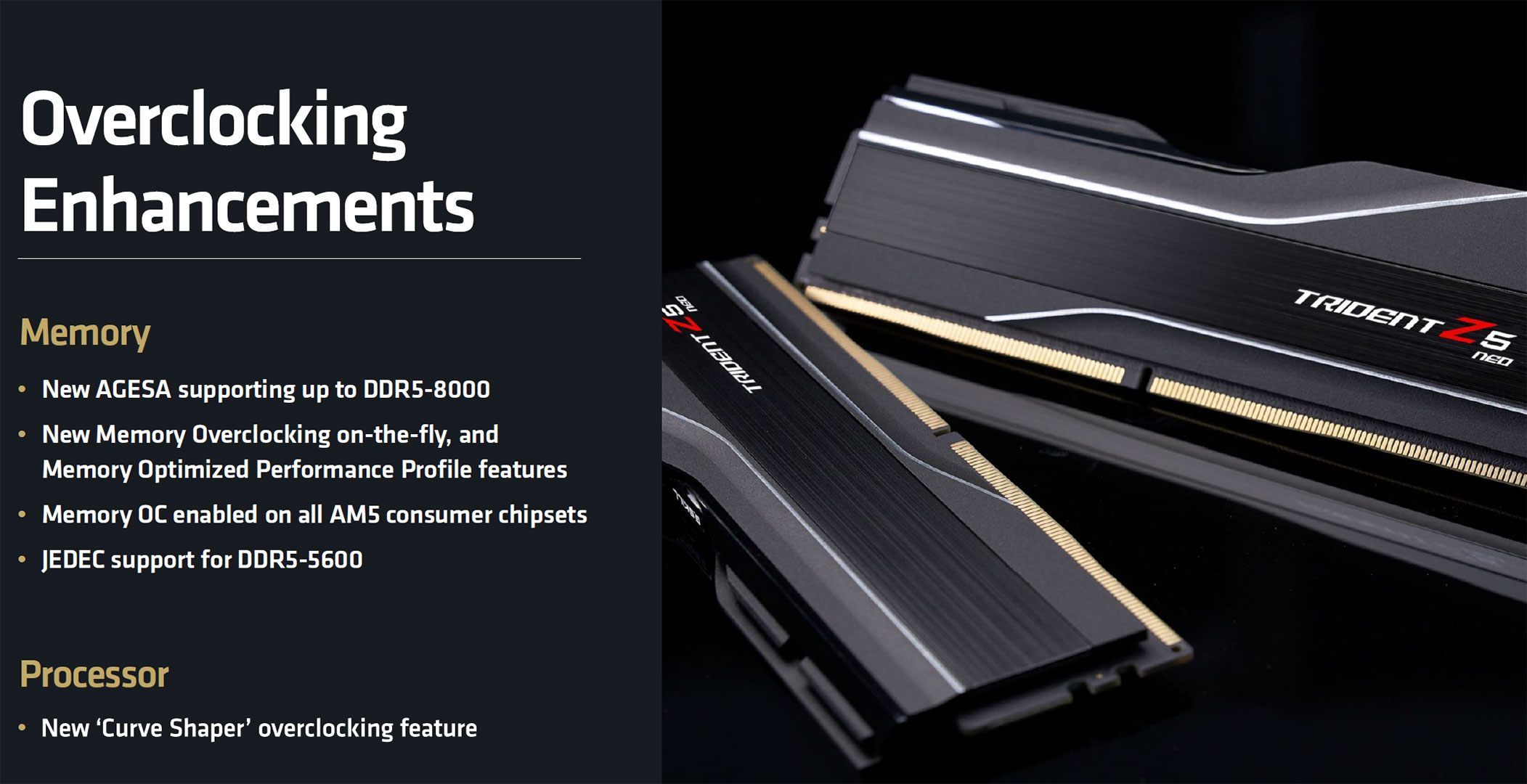
Native DDR5 support has been increased to DDR5-5600, and support has been added for overclocked memory as fast as DDR5-8000. To achieve this, a 1:2 clock divider is engaged between FCLK and MCLK as soon as memory clock is set higher than DDR5-6000. You may manually force a 1:1 divider "and with some luck" you will be able to run DDR5-6400—essentially the same as with Zen 4. DDR5-8000 support has been released by AMD through an update to the AGESA microcode, for motherboard vendors to integrate with even their older AMD 600-series chipset products. There should be a new wave of enthusiast PC memory with AMD EXPO profiles for DDR5-8000 and everything under (such as DDR5-7200, DDR5-6800, etc.). In terms of performance it is interesting to see if DDR5-8000 1:2 can beat DDR5-6000 1:1 in a wide range of scenarios, which could make it a worthwhile investment. TPU has tested Zen 5 memory scaling in a separate article.
Socket AM5


Here are a few pictures of Socket AM5, the star-attraction with this platform. This is a land-grid array (LGA) socket with 1,718 pins.

As with every LGA socket, the pins are on the motherboard, whereas the processor package has contacts that interface with those pins, while a retention brace holds the package in place with a locking lever. Installing a processor on AM5 is similar to doing so on any of the dozens of Intel LGA sockets.


On Socket AM4, removing the four mounting screws resulted in the backplate falling off, which meant you needed three hands when installing a cooler, and several vendors also bundled their own backplates. On Socket AM5 the backplate isn't designed to be removed, which makes cooler installation MUCH easier.

The caps for the socket are not identical to the Intel LGA sockets, so you can't reuse them.
Unboxing and Photography

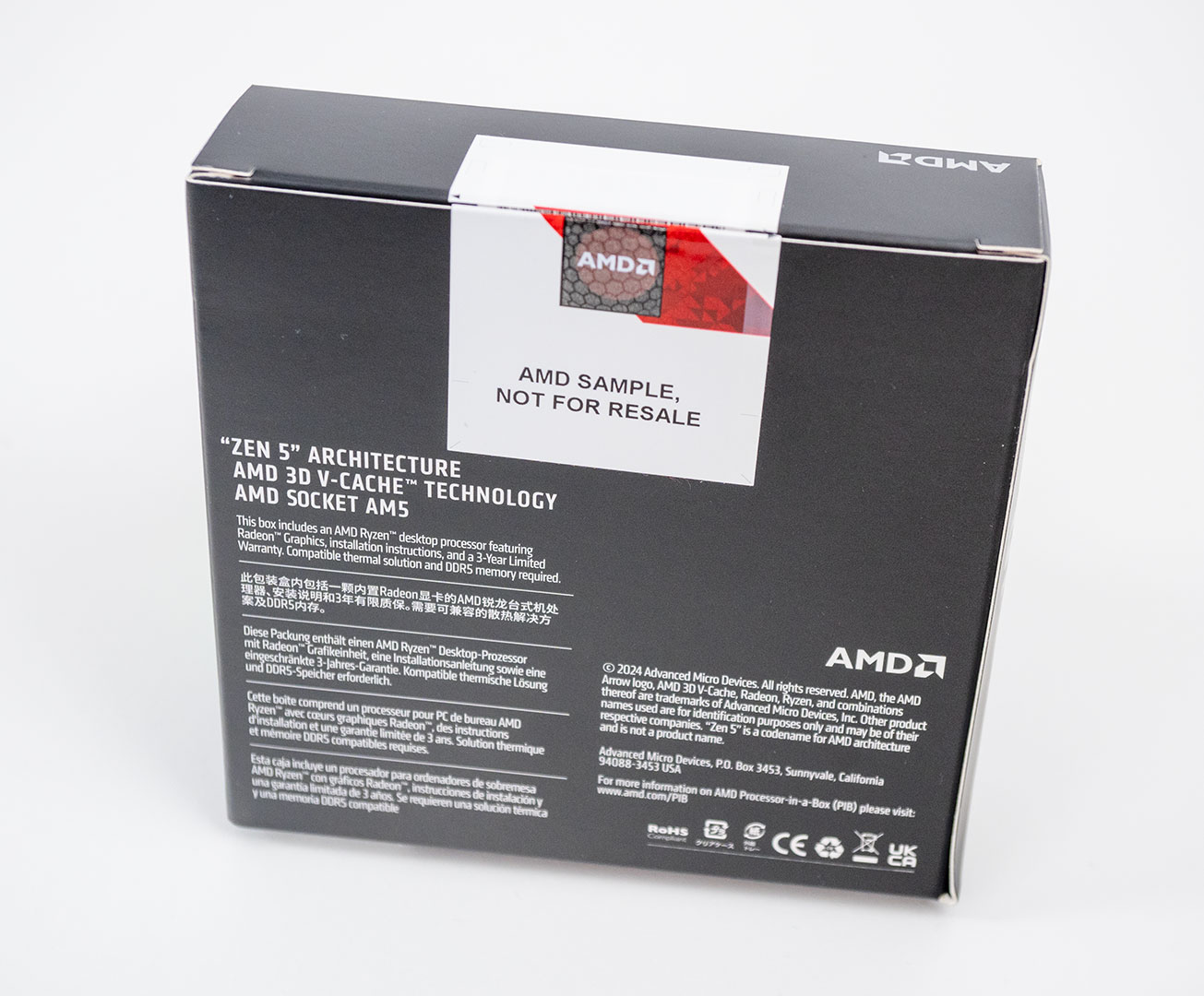
The Ryzen 9 9950X3D comes in a square-shaped box, similar to the other Ryzen 9000 series chips. There's no included cooling solution. The box-art is a slight variation on the theme set by the regular Ryzen 9000 series chips, the AMD arrow is now set against a silver backdrop instead of gray. There's clear marking on the front and back faces that the processor features 3D V-Cache technology.


The Ryzen 9000 Series looks just like the previous Ryzen 7000 Socket AM5 processors. While there are some minimal changes to the SMD capacitor layout, these aren't significant in any way.

The AM5 socket retention brace only applies pressure along the two side protrusions of the IHS. Intel sockets have it the same way. Socket AM5 retains cooler compatibility with AM4, so you're spoiled for choice with aftermarket cooling solutions.
Our Patreon Silver Supporters can read articles in single-page format.
Mar 12th, 2025 20:44 EDT
change timezone
Latest GPU Drivers
New Forum Posts
- Bright Memory: Infinite Ray Tracing Benchmark (21)
- I'm looking for a good tool to make the 3D scanning of my mini-pc using the photogrammetry and my Kinect 2. (76)
- What motherboard with spdif should I get? PC to 5.1 blu-ray player via optical (7)
- What else can I do to diagnose an artifacting card? (2)
- Post your Old CDs & FDs, from back in the day thread. (67)
- RTX 3060 black screens on load and light browsing even after RMA (25)
- Packet Loss after updating to windows 11 (10)
- Zen6 is almost here ? (60)
- HOW TO ADD NVMe M.2 SSD SUPPORT TO OLD MOTHERBOARDS WITH AMI BIOS LEGACY SUPPORT? (7)
- Shadow of the Tomb Raider benchmark (539)
Popular Reviews
- AMD Ryzen 9 9950X3D Review - Great for Gaming and Productivity
- XFX Radeon RX 9070 XT Mercury OC Magnetic Air Review
- Sapphire Radeon RX 9070 XT Nitro+ Review - Beating NVIDIA
- Dough Spectrum Black 32 Review
- ASUS Radeon RX 9070 TUF OC Review
- FSP MP7 Black Review
- AMD Ryzen 7 9800X3D Review - The Best Gaming Processor
- NVIDIA GeForce RTX 5070 Founders Edition Review
- MSI MAG B850 Tomahawk Max Wi-Fi Review
- XPG Starker Air BTF Review
Controversial News Posts
- NVIDIA GeForce RTX 50 Cards Spotted with Missing ROPs, NVIDIA Confirms the Issue, Multiple Vendors Affected (513)
- AMD Radeon RX 9070 and 9070 XT Listed On Amazon - One Buyer Snags a Unit (261)
- AMD RDNA 4 and Radeon RX 9070 Series Unveiled: $549 & $599 (260)
- AMD Mentions Sub-$700 Pricing for Radeon RX 9070 GPU Series, Looks Like NV Minus $50 Again (249)
- NVIDIA Investigates GeForce RTX 50 Series "Blackwell" Black Screen and BSOD Issues (244)
- AMD Radeon RX 9070 and 9070 XT Official Performance Metrics Leaked, +42% 4K Performance Over Radeon RX 7900 GRE (195)
- AMD Radeon RX 9070-series Pricing Leaks Courtesy of MicroCenter (158)
- AMD Radeon RX 9070 XT Reportedly Outperforms RTX 5080 Through Undervolting (101)