 28
28
ASUS GeForce RTX 5070 TUF OC Review
(28 Comments) »Introduction
The ASUS GeForce RTX 5070 TUF OC is a premium, factory-overclocked variant of NVIDIA's latest performance-segment GPU. Engineered for high-performance gaming, it features a powerful cooling solution, dual BIOS with a quiet mode, and customizable RGB lighting. The TUF series is known for its high-quality components, excellent thermal efficiency, and sleek design, making it a top choice for enthusiasts who want to go beyond the basic designs at MSRP.

The RTX 5070 is a key release in NVIDIA's Blackwell architecture, offering high-refresh-rate 1080p gameplay and fully ray-traced 1440p experiences. It introduces Neural Rendering, a technology that integrates AI-generated objects into traditional 3D graphics, enhancing realism. The AI Management Processor (AMP) enables seamless coordination between AI workloads and conventional rendering, improving overall efficiency.
Built on the GB205 GPU, the RTX 5070 features 48 out of 50 active streaming multiprocessors, delivering 6,144 CUDA cores, 192 Tensor cores, 48 RT cores, and 192 texture units. It also includes 80 ROPs, an upgrade from the RTX 4070's 64. The GPU benefits from 48 MB of L2 cache, up from 36 MB in the previous generation. While it retains 12 GB of VRAM, the switch to 28 Gbps GDDR7 memory increases bandwidth by 33%, enhancing performance.
ASUS has equipped the TUF OC with an advanced cooling system, including a large heatsink, a triple-fan design, and a nickel-plated copper baseplate for efficient heat dissipation. The dual BIOS allows users to toggle between performance and quiet modes, providing flexibility based on cooling and noise preferences. The factory overclock ensures higher clock speeds out of the box, maximizing performance.
With its premium design, high-end cooling, and customizable RGB lighting, the ASUS GeForce RTX 5070 TUF OC is an excellent choice for gamers seeking top-tier performance and aesthetics. It ticks at a rated boost clock of 2610 MHz and is priced at $740, which is a $190(!) increase over the NVIDIA MSRP.
| Price | Cores | ROPs | Core Clock | Boost Clock | Memory Clock | GPU | Transistors | Memory | |
|---|---|---|---|---|---|---|---|---|---|
| RTX 3080 | $420 | 8704 | 96 | 1440 MHz | 1710 MHz | 1188 MHz | GA102 | 28000M | 10 GB, GDDR6X, 320-bit |
| RTX 4070 | $490 | 5888 | 64 | 1920 MHz | 2475 MHz | 1313 MHz | AD104 | 35800M | 12 GB, GDDR6X, 192-bit |
| RX 7800 XT | $440 | 3840 | 96 | 2124 MHz | 2430 MHz | 2425 MHz | Navi 32 | 28100M | 16 GB, GDDR6, 256-bit |
| RX 6900 XT | $450 | 5120 | 128 | 2015 MHz | 2250 MHz | 2000 MHz | Navi 21 | 26800M | 16 GB, GDDR6, 256-bit |
| RX 6950 XT | $630 | 5120 | 128 | 2100 MHz | 2310 MHz | 2250 MHz | Navi 21 | 26800M | 16 GB, GDDR6, 256-bit |
| RTX 3090 | $900 | 10496 | 112 | 1395 MHz | 1695 MHz | 1219 MHz | GA102 | 28000M | 24 GB, GDDR6X, 384-bit |
| RTX 4070 Super | $590 | 7168 | 80 | 1980 MHz | 2475 MHz | 1313 MHz | AD104 | 35800M | 12 GB, GDDR6X, 192-bit |
| RX 7900 GRE | $530 | 5120 | 160 | 1880 MHz | 2245 MHz | 2250 MHz | Navi 31 | 57700M | 16 GB, GDDR6, 256-bit |
| RTX 4070 Ti | $700 | 7680 | 80 | 2310 MHz | 2610 MHz | 1313 MHz | AD104 | 35800M | 12 GB, GDDR6X, 192-bit |
| RTX 5070 | $550 | 6144 | 80 | 2325 MHz | 2512 MHz | 1750 MHz | GB205 | 31100M | 12 GB, GDDR7, 192-bit |
| ASUS RTX 5070 TUF OC | $740 | 6144 | 80 | 2325 MHz | 2610 MHz | 1750 MHz | GB205 | 31100M | 12 GB, GDDR7, 192-bit |
| RTX 4070 Ti Super | $750 | 8448 | 112 | 2340 MHz | 2610 MHz | 1313 MHz | AD103 | 45900M | 16 GB, GDDR6X, 256-bit |
| RX 7900 XT | $620 | 5376 | 192 | 2000 MHz | 2400 MHz | 2500 MHz | Navi 31 | 57700M | 20 GB, GDDR6, 320-bit |
| RTX 5070 Ti | $750 | 8960 | 96 | 2295 MHz | 2452 MHz | 1750 MHz | GB203 | 45600M | 16 GB, GDDR7, 256-bit |
| RTX 3090 Ti | $1000 | 10752 | 112 | 1560 MHz | 1950 MHz | 1313 MHz | GA102 | 28000M | 24 GB, GDDR6X, 384-bit |
| RTX 4080 | $940 | 9728 | 112 | 2205 MHz | 2505 MHz | 1400 MHz | AD103 | 45900M | 16 GB, GDDR6X, 256-bit |
| RTX 4080 Super | $990 | 10240 | 112 | 2295 MHz | 2550 MHz | 1438 MHz | AD103 | 45900M | 16 GB, GDDR6X, 256-bit |
| RX 7900 XTX | $820 | 6144 | 192 | 2300 MHz | 2500 MHz | 2500 MHz | Navi 31 | 57700M | 24 GB, GDDR6, 384-bit |
| RTX 5080 | $1000 | 10752 | 112 | 2295 MHz | 2617 MHz | 1875 MHz | GB203 | 45600M | 16 GB, GDDR7, 256-bit |
| RTX 4090 | $2400 | 16384 | 176 | 2235 MHz | 2520 MHz | 1313 MHz | AD102 | 76300M | 24 GB, GDDR6X, 384-bit |
| RTX 5090 | $2000 | 21760 | 176 | 2017 MHz | 2407 MHz | 1750 MHz | GB202 | 92200M | 32 GB, GDDR7, 512-bit |
NVIDIA Blackwell Architecture
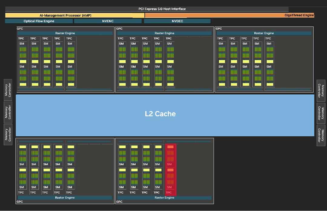
NVIDIA does not provide a block diagram for the GB205 GPU (we asked), so we had to quickly hack one out from the GB202 diagram. This is accurate just not as pretty.
The GeForce Blackwell graphics architecture heralds NVIDIA's 4th generation of RTX, the late-2010s re-invention of the modern GPU that sees a fusion of real time ray traced objects with conventional raster 3D graphics. With Blackwell, NVIDIA is helping add another dimension, neural rendering, the ability for the GPU to leverage a generative AI to create portions of a frame. This is different from DLSS, where an AI model is used to reconstruct details in an upscaled frame based on its training date, temporal frames, and motion vectors. Today we are reviewing NVIDIA's fourth GPU from this generation, the RTX 5070. At the heart of this graphics card is the new 5 nm GB205 silicon. This chip has a unique die-size and SM count that doesn't have a predecessor from the previous Ada generation. NVIDIA skipped a direct successor to the AD104 in the Blackwell generation, instead building the RTX 5070 Ti on the larger GB203 silicon and the RTX 5070 on the technically smaller GB205. The chip measures 263 mm² in die-area, with a transistor count of 31.1 billion, both of which are smaller than those of the AD104, which had to part with nearly a fifth of its shaders to yield an RTX 4070. Given its volumes, NVIDIA would probably have had to part with perfectly good AD104 chips to carve out the RTX 4070. It's to minimize this die area wastage in this generation that the company set out to create the GB205.
The GB205 silicon is laid out essentially in the same component hierarchy as past generations of NVIDIA GPUs, but with a few notable changes. The GPU features a PCI-Express 5.0 x16 host interface. PCIe Gen 5 has been around since Intel's 12th Gen Core "Alder Lake" and AMD's Ryzen 7000 "Zen 4," so there is a sizable install-base of systems that can take advantage of it. The GPU is of course compatible with older generations of PCIe. The GB205 also features the new GDDR7 memory interface that's making its debut with this generation. The chip features a 192-bit wide memory bus. NVIDIA is using this to drive 12 GB of memory at 28 Gbps speeds, yielding 672 GB/s of memory bandwidth, which is a 33% increase over the RTX 4070 and its 21 Gbps GDDR6X.
The GigaThread Engine is the main graphics rendering workload allocation logic on the GB205, but there's a new addition, a dedicated serial processor for managing all AI acceleration resources on the GPU, NVIDIA calls this AMP (AI management processor). Other components at the global level are the Optical Flow Processor, a component involved in older versions of DLSS frame generation and for video encoding; and an updated media acceleration engine consisting of one each of NVDEC and NVENC video accelerators. The new 9th Gen NVENC video encode accelerators come with 4:2:2 AV1 and HEVC encoding support. The central region of the GPU has the single largest common component, the 48 MB L2 cache, which the RTX 5070 maxes out. This is an increase over the 36 MB that the RTX 4070 has.

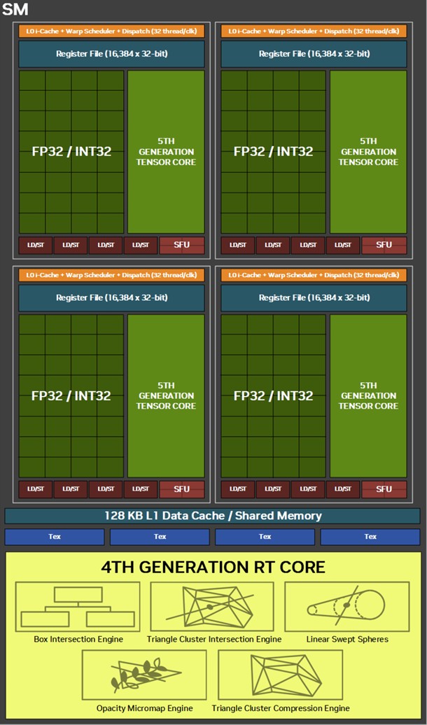
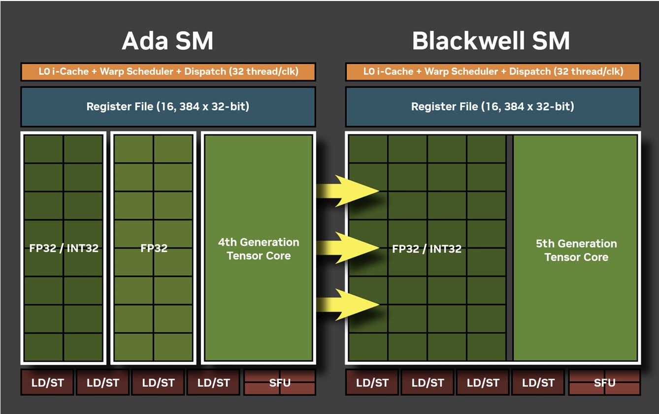
There are five graphics processing clusters (GPC) on the GB205. Each of these contains 10 streaming multiprocessors (SM) across 5 texture processing clusters (TPCs), and a raster engine consisting of 16 ROPs. Each SM contains 128 CUDA cores. Unlike the Ada generation SM that each had 64 FP32+INT32 and 64 purely-FP32 SIMD units, the new Blackwell generation SM features concurrent FP32+INT32 capability on all 128 SIMD units. These 128 CUDA cores are arranged in four slices, each with a register file, a level-0 instruction cache, a warp scheduler, two sets of load-store units, and a special function unit (SFU) handling some special math functions such as trigonometry, exponents, logarithms, reciprocals, and square-root. The four slices share a 128 KB L1 data cache, and four TMUs. The most exotic components of the Blackwell SM are the four 5th Gen Tensor cores, and a 4th Gen RT core.
With 5 GPCs containing 5 TPCs each, there are a total of 50 SM, worth 6,400 CUDA cores, 200 Tensor cores, 50 RT cores, and 200 TMUs, on the GB205 silicon. The RTX 5070 doesn't max out the silicon, it gets 48 out of the 50 SM, resulting in 6,144 CUDA cores, 192 Tensor cores, 48 RT cores, and 192 TMUs. The GB205 silicon is endowed with 80 ROPs, all of which are enabled on the RTX 5070. This is a step up from the RTX 4070, which only had 64 out of 80 ROPs present on the AD104 silicon. The RTX 5070 also maxes out all 48 MB of L2 cache present on the die, while the RTX 4070 only had 36 MB out of the 48 MB present.
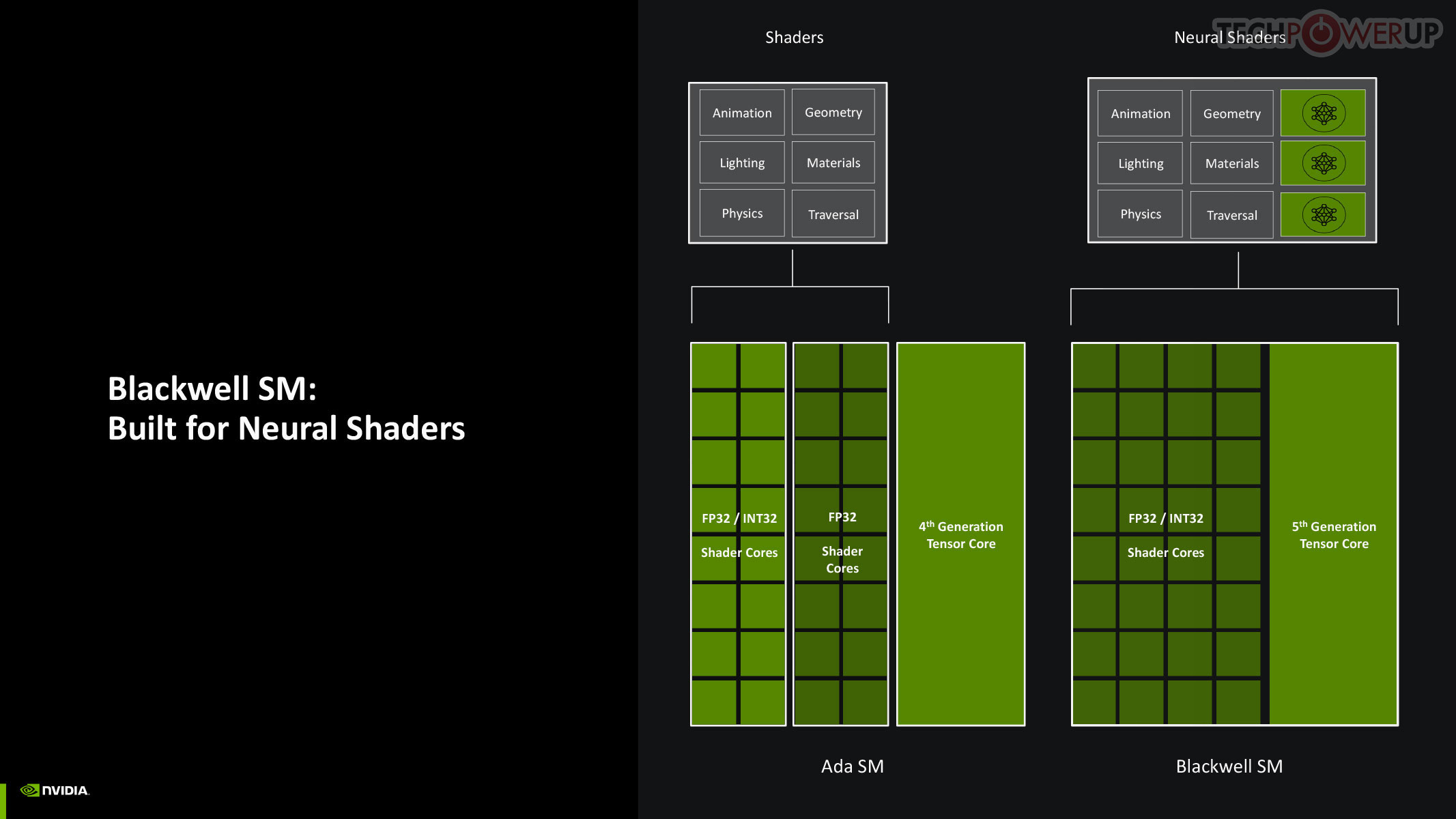
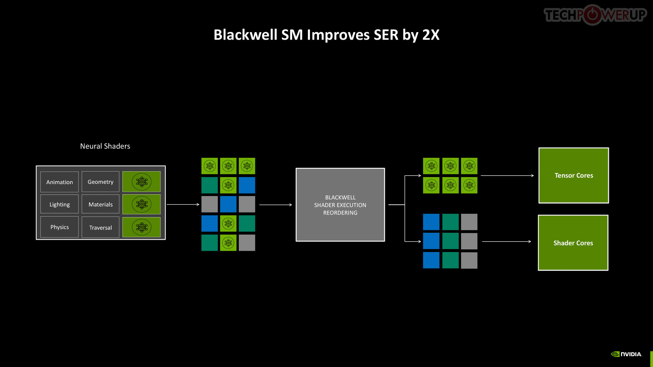
Perhaps the biggest change to the way the SM handles work introduced with Blackwell is the concept of neural shaders—treating portions of the graphics rendering workload done by a generative AI model as shaders. Microsoft has laid the groundwork for standardization of neural shaders with its Cooperative Vectors API, in the latest update to DirectX 12. The Tensor cores are now accessible for workloads through neural shaders, and the shader execution reordering (SER) engine of the Blackwell SM is able to more accurately reorder workloads for the CUDA cores and the Tensor core in an SM.
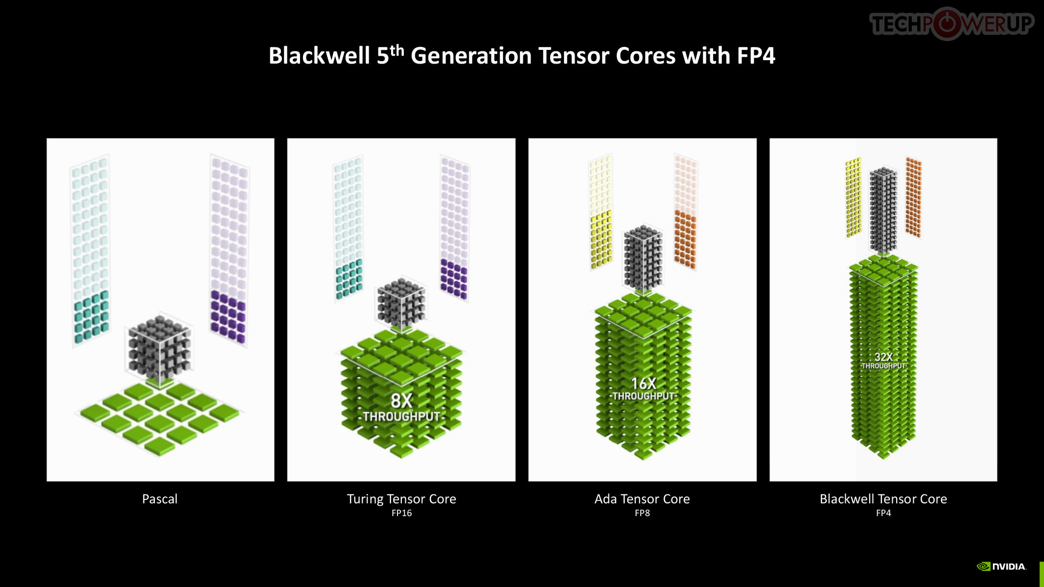
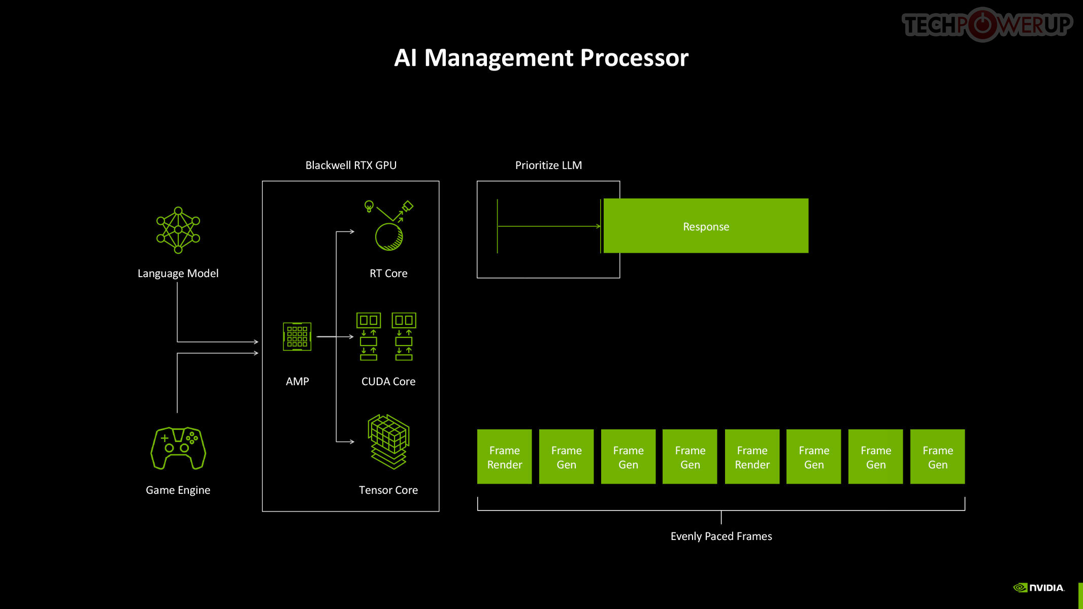
The new 5th Gen Tensor core introduces support for FP4 data format (1/8 precision) to fast moving atomic workloads, providing 32 times the throughput of the very first Tensor core introduced with the Volta architecture. Over the generations, AI models leveraged lesser precision data formats, and sparsity, to improve performance. The AI management processor (AMP) is what enables simultaneous AI and graphics workloads at the highest levels of the GPU, so it could be simultaneously rendering real time graphics for a game, while running an LLM, without either affecting the performance of the other. AMP is a specialized hardware scheduler for all the AI acceleration resources on the silicon. This plays a crucial role for DLSS 4 multi-frame generation to work.
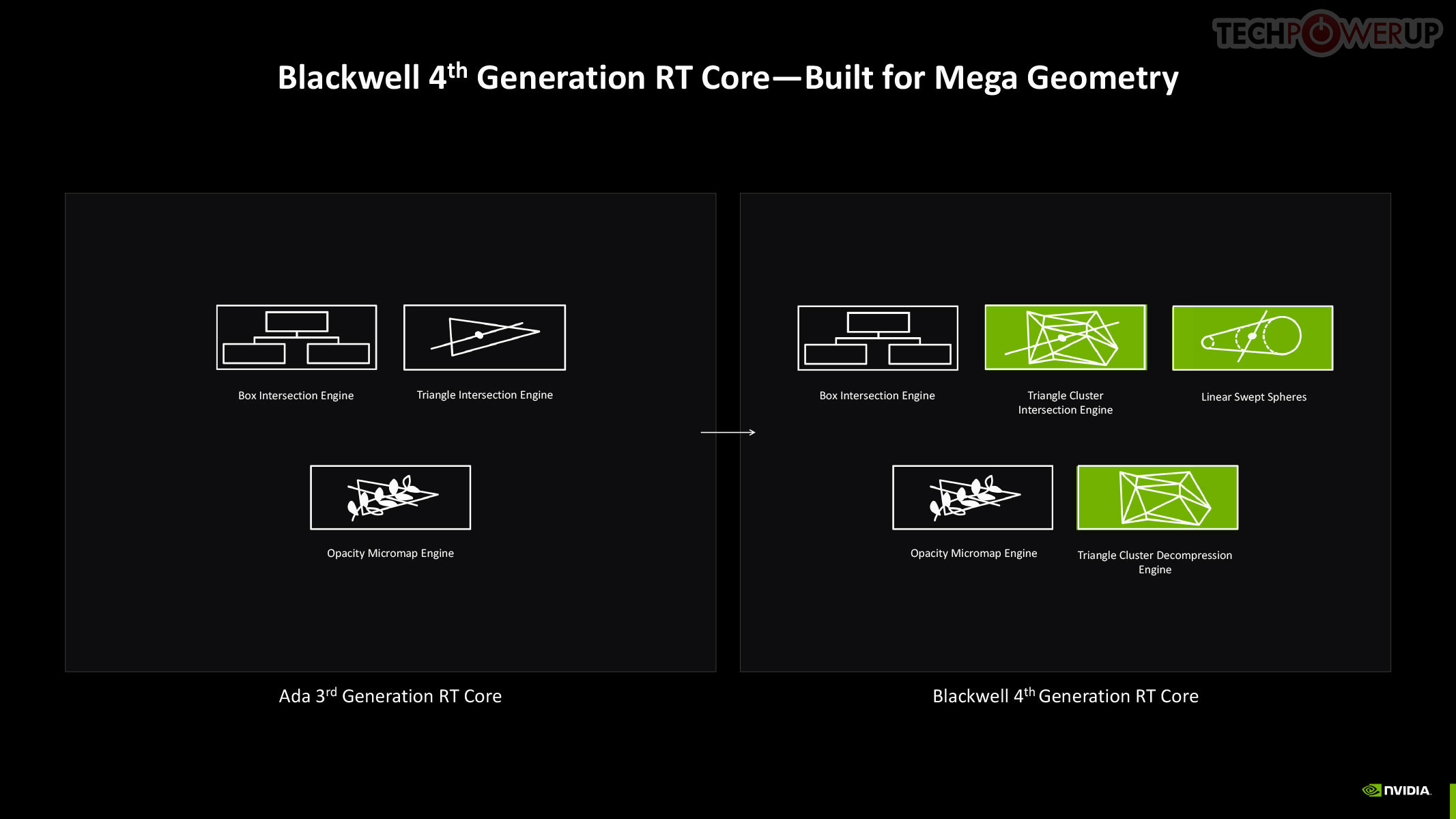
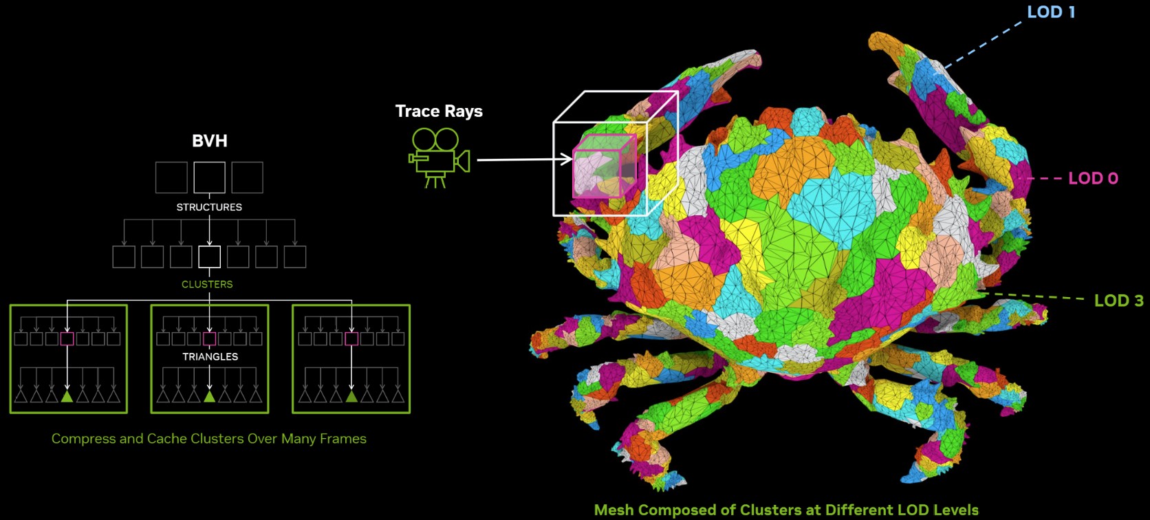
The 4th Gen RT core not just offers a generational increase in ray testing and ray intersection performance, which lowers the performance cost of enabling path tracing and ray traced effects; but also offers a potential generational leap in performance with the introduction of Mega Geometry. This allows for ray traced objects with extremely high polygon counts, increasing their detail. Poly count and ray tracing present linear increases in performance costs, as each triangle has to intersect with a ray, and there should be sufficient rays to intersect with each of them. This is achieved by adopting clusters of triangles in an object as first-class primitives, and cluster-level acceleration structures. The new RT cores introduce a component called a triangle cluster intersection engine, designed specifically for handling mega geometry. The integration of a triangle cluster compression format and a lossless decompression engine allows for more efficient processing of complex geometry.
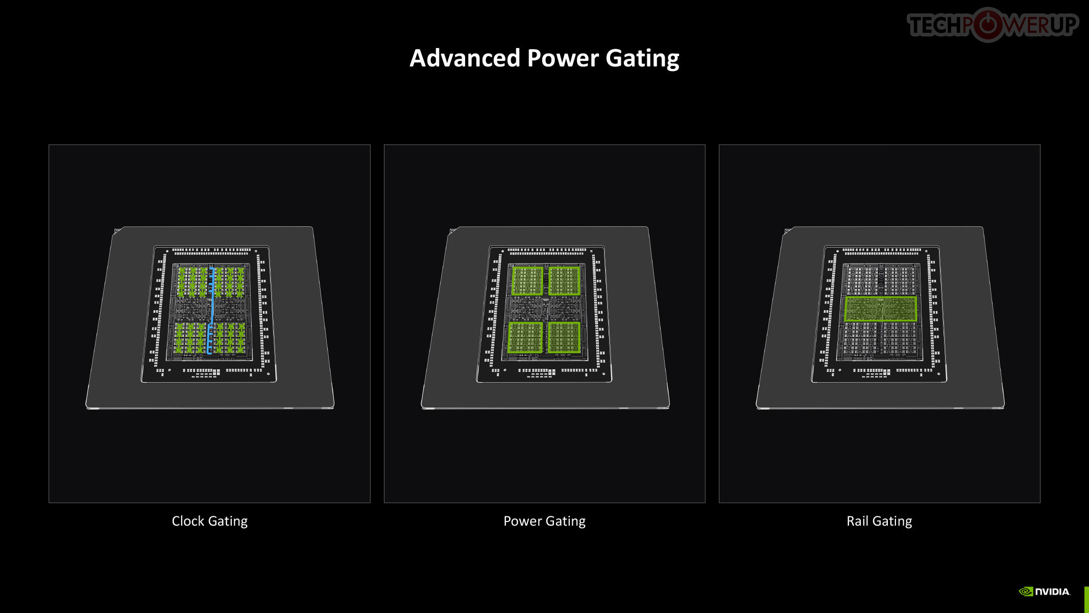
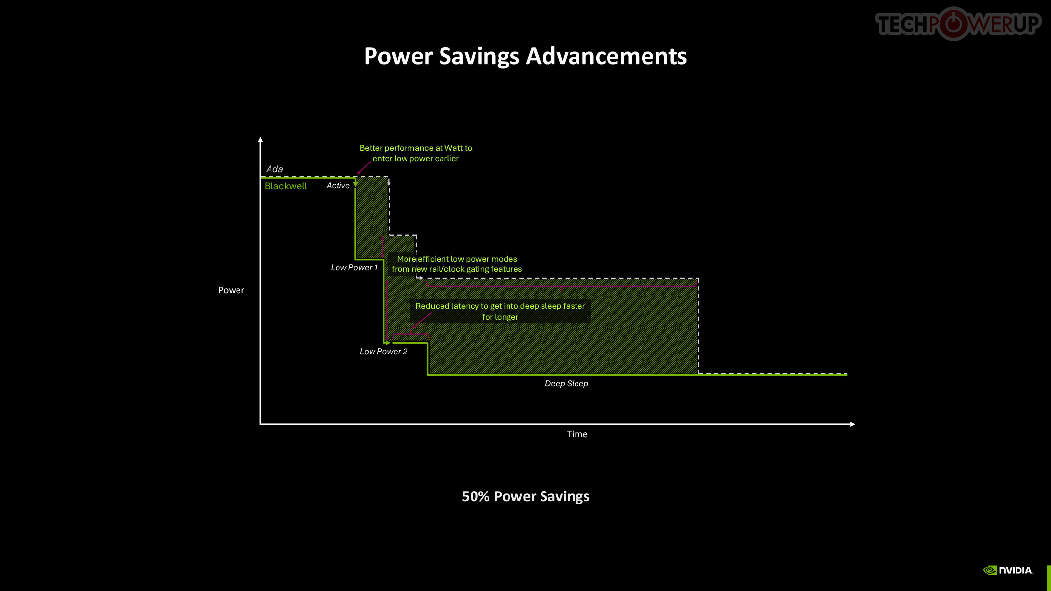
The GB205 and the rest of the GeForce Blackwell GPU family is built on the exact same TSMC "NVIDIA 4N" foundry node, which is actually 5 nm, as previous-generation Ada, so NVIDIA directed efforts to finding innovative new ways to manage power and thermals. This is done through a re-architected power management engine that relies on clock gating, power gating, and rail gating of the individual GPCs and other top-level components. It also worked on the speed at which the GPU makes power-related decisions.
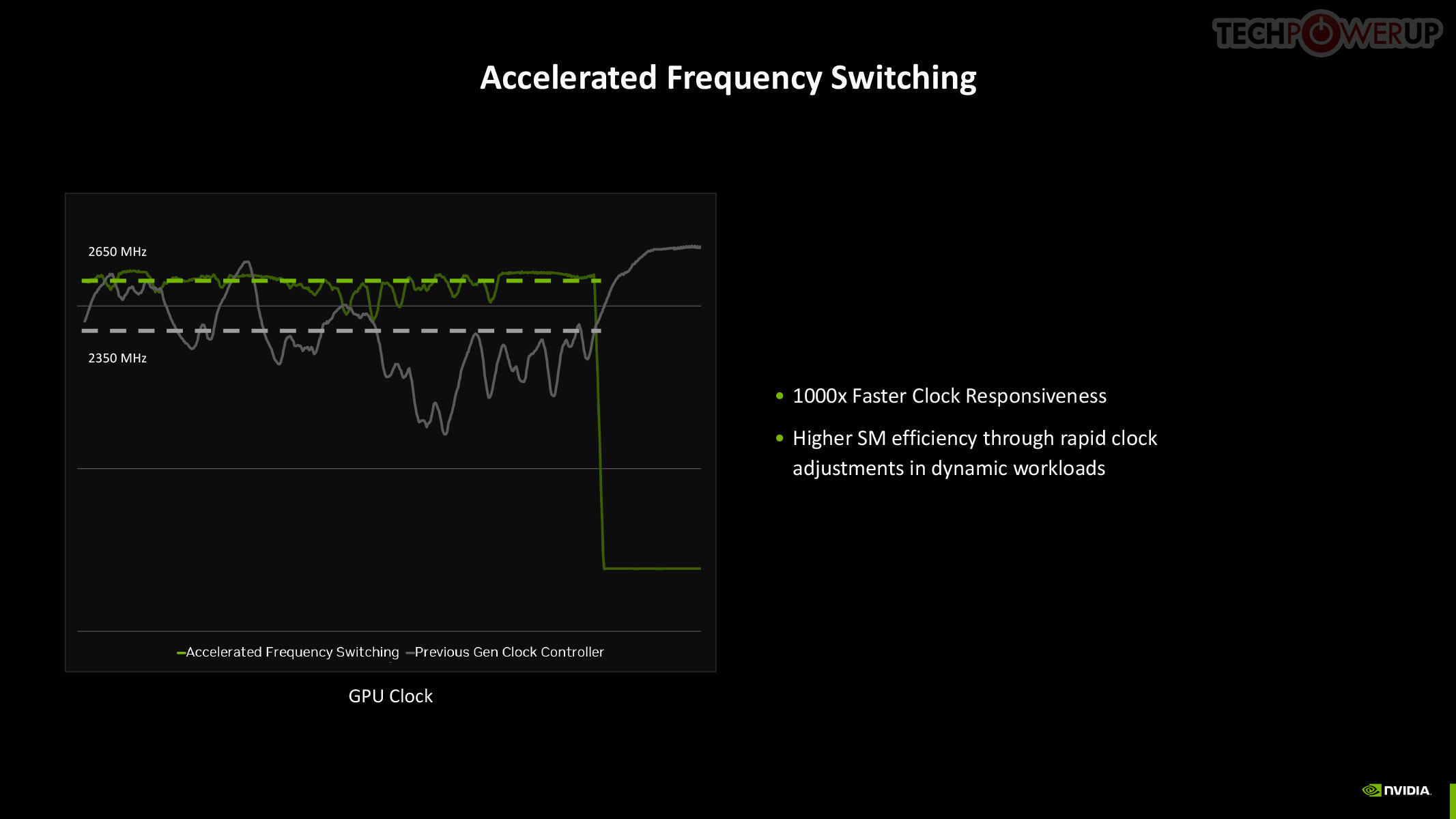
The quickest way to drop power is by adjusting the GPU clock speed, and with Blackwell, NVIDIA introduced a means for rapid clock adjustments at the SM-level.
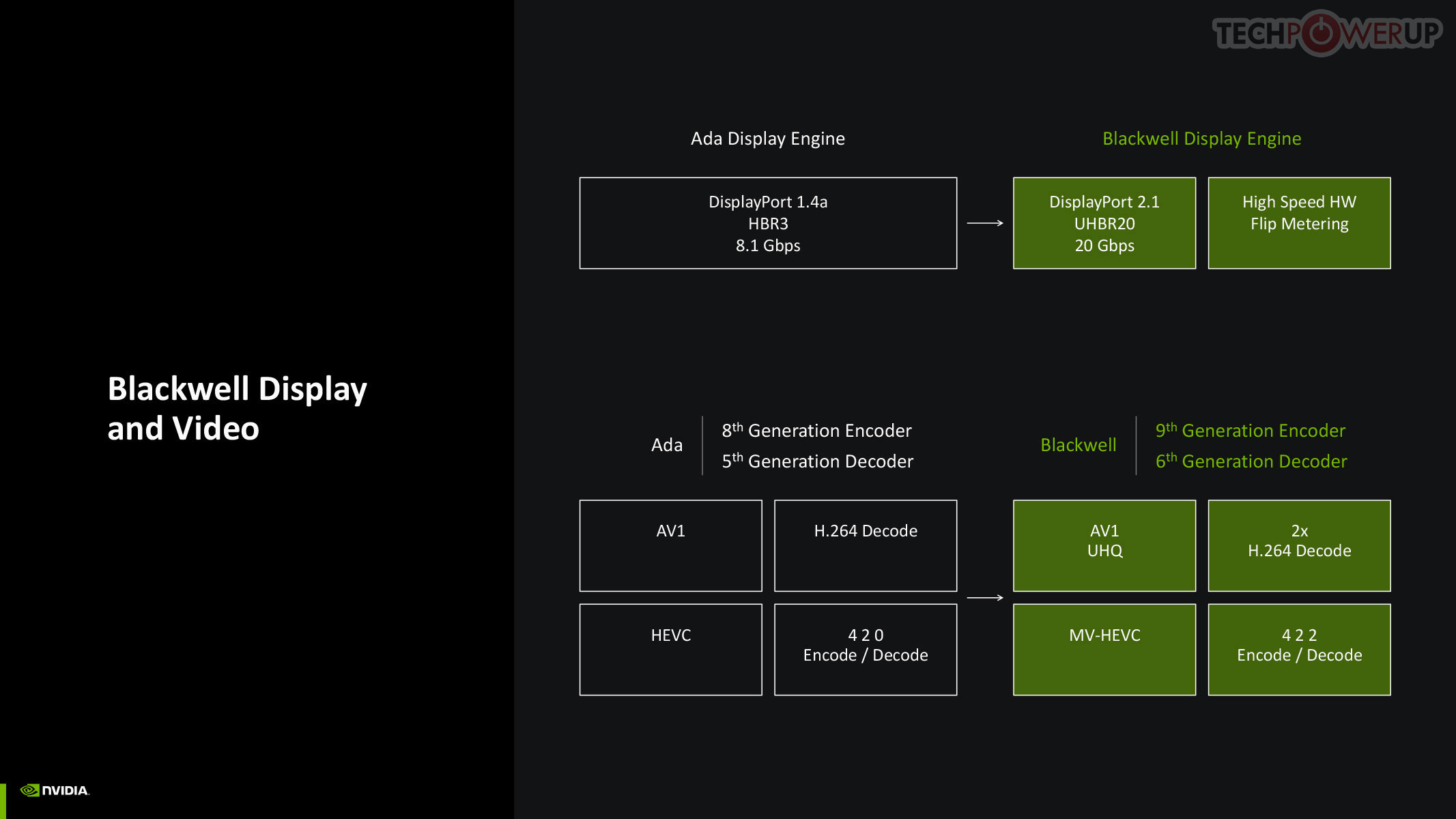
NVIDIA updated both the display engine and the media engine of Blackwell over the previous generation Ada, which drew some flack for holding on to older display I/O standards such as DisplayPort 1.4, while AMD and Intel had moved on to DisplayPort 2.1. The good news is that Blackwell supports DP 2.1 with UHBR20, enabling 8K 60 Hz with a single cable. The company also updated NVDEC and NVENC, which now support AV1 UHQ, double the H.264 decode performance, MV-HEVC, and 4:2:2 formats.
Neural Rendering
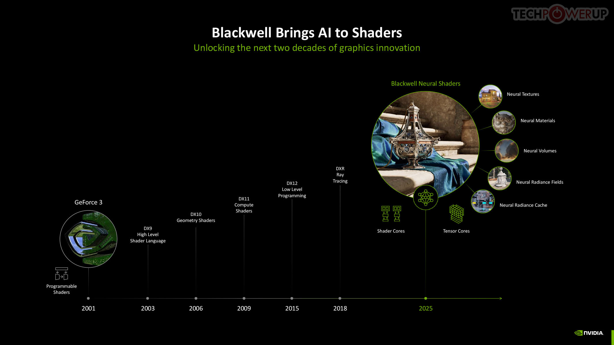
Neural Rendering promises to be as transformative to modern graphics as programmable shaders itself. 3D Graphics rendering evolved from fixed-function over the turn of the century, to programmable shaders, HLSL, geometry shaders, compute shaders, and ray tracing, over the past couple of decades. In 2025, NVIDIA is writing the next chapter in this journey with Blackwell neural shaders. This allows for a host of neural-driven effects, including neural materials, neural volumes, and even neural radiance fields. Microsoft introduced the new Cooperative Vectors API for DirectX in a recent update, making it possible to access Tensor cores within a graphics API. Combined with a new shading language, Slang, this breakthrough enables developers to integrate neural techniques directly into their workflows, potentially replacing parts of the traditional graphics pipeline. Slang splits large, complex functions into smaller pieces that are easier to handle. Given that this is a DirectX standard API feature, there is nothing that stops AMD and Intel from integrating Neural Rendering (Cooperative Vectors) into their graphics drivers.
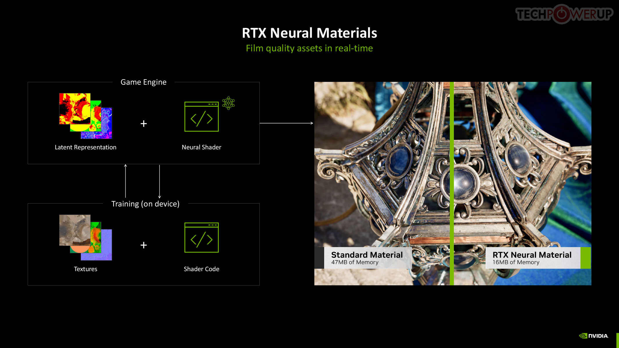
RTX Neural Materials works to significantly reduce the memory footprint of materials in 3D scenes. Under conventional rendering, the memory footprint of a material is bloated from complex shader code. Neural materials convert shader code and texture layers into a compressed neural representation. This results in up to a 7:1 compression ratio and enables small neural networks to generate stunning, film-like materials in real-time. For example, silk rendered with traditional shaders might lack the multicolored sheen seen in real life. Neural materials, however, capture intricate details like color variation and reflections, bringing such surfaces to life with unparalleled realism—and at a fraction of the memory cost.
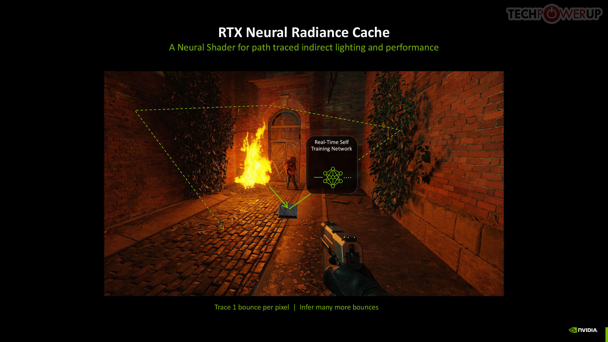
The new Neural Radiance Cache, which dynamically trains a neural network during gameplay using the user's GPU, allowing light transport to be cached spatially, enabling near-infinite light bounces in a scene. This results in realistic indirect lighting and shadows with minimal performance impact. NRC partially traces 1 or 2 rays before storing them in a radiance cache, and infers an infinite amount of rays and bounces for a more accurate representation of indirect lighting in the game scene.
DLSS 4 and Multi Frame Generation
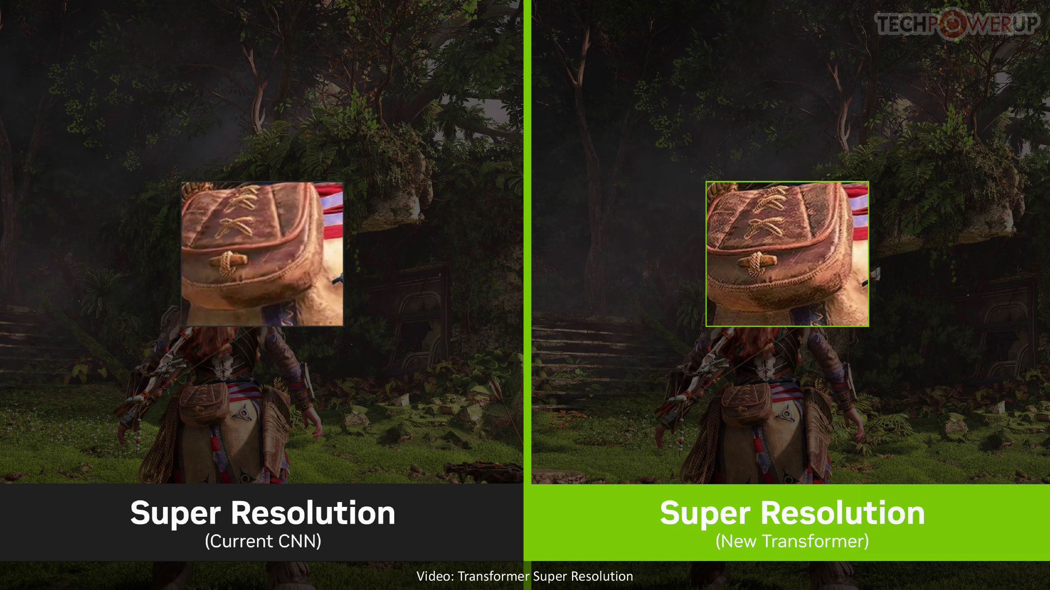
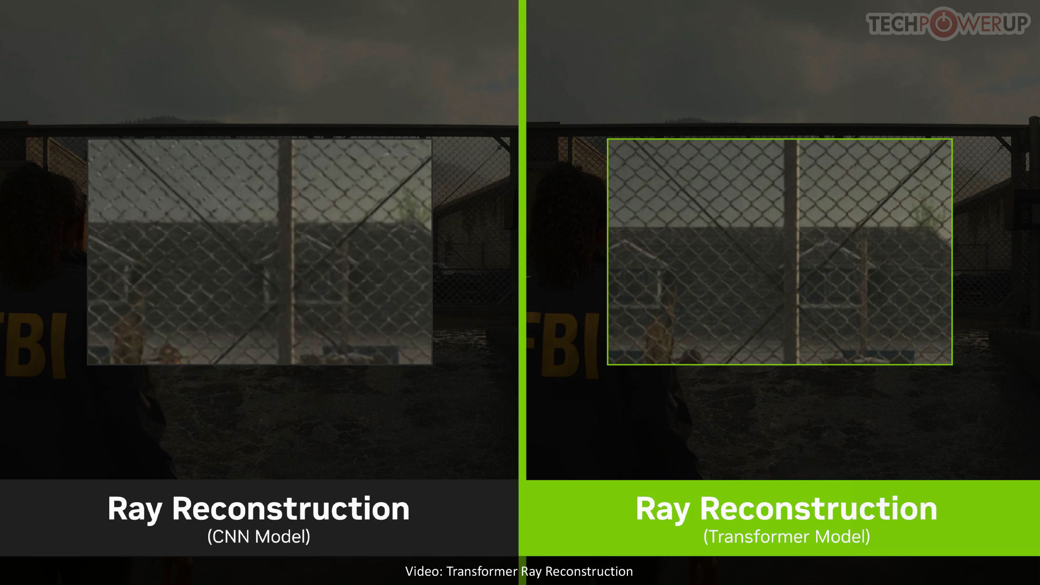
DLSS 4 introduces a major leap in image quality and performance. It isn't just a version bump with the introduction of a new feature, namely Multi Frame Generation, but introduces updates to nearly all DLSS sub-features. DLSS from its very beginning relied on AI to reconstruct details in super resolution, and with DLSS 4, NVIDIA is introducing a new transformer-based AI model to succeed the convolutional neural networks previous used, for double the parameters, four times the compute performance, and significantly improved image quality. Ray Reconstruction, introduced with DLSS 3.5, gets a significant image quality update with the new transformer-based model.
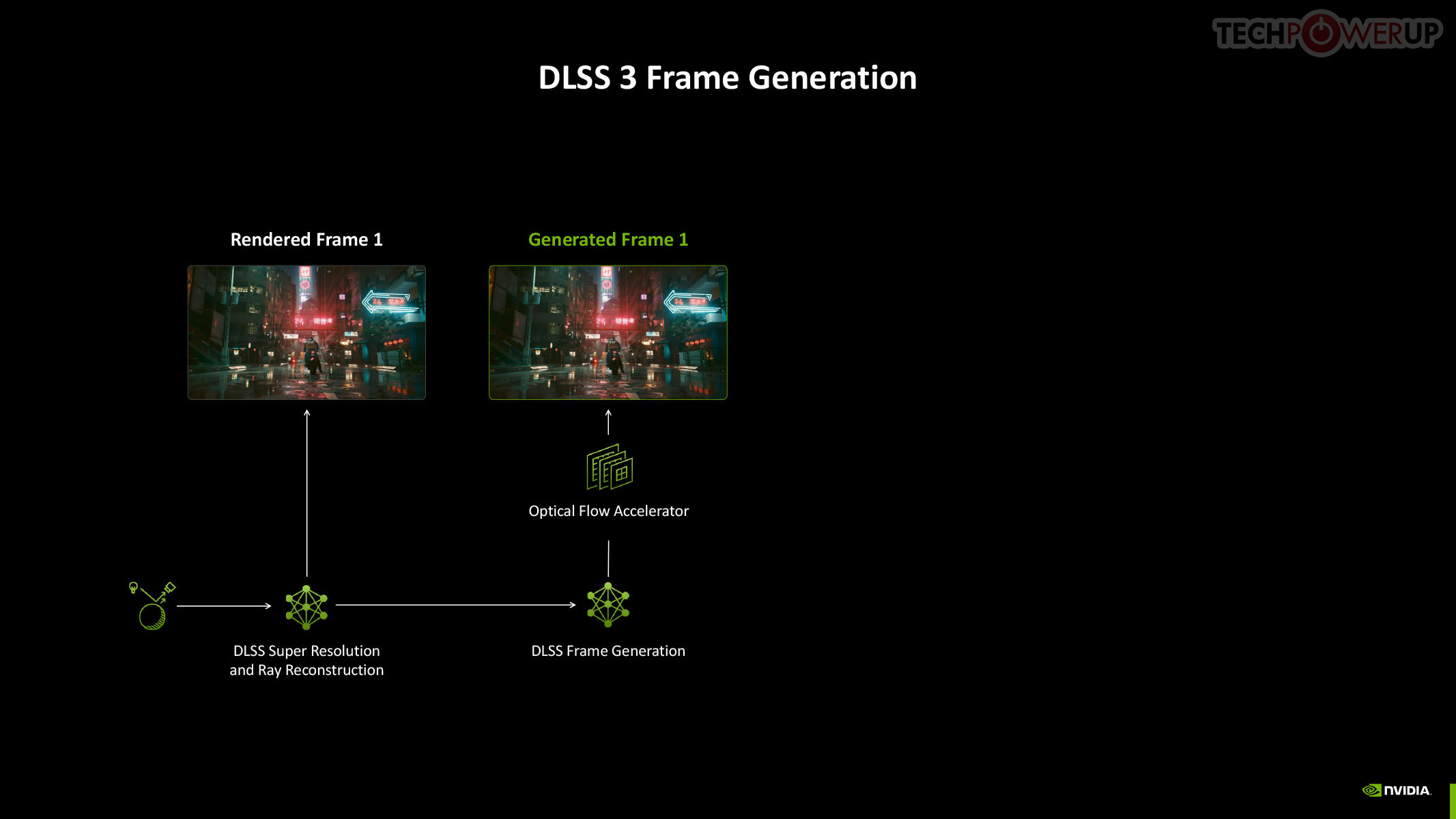
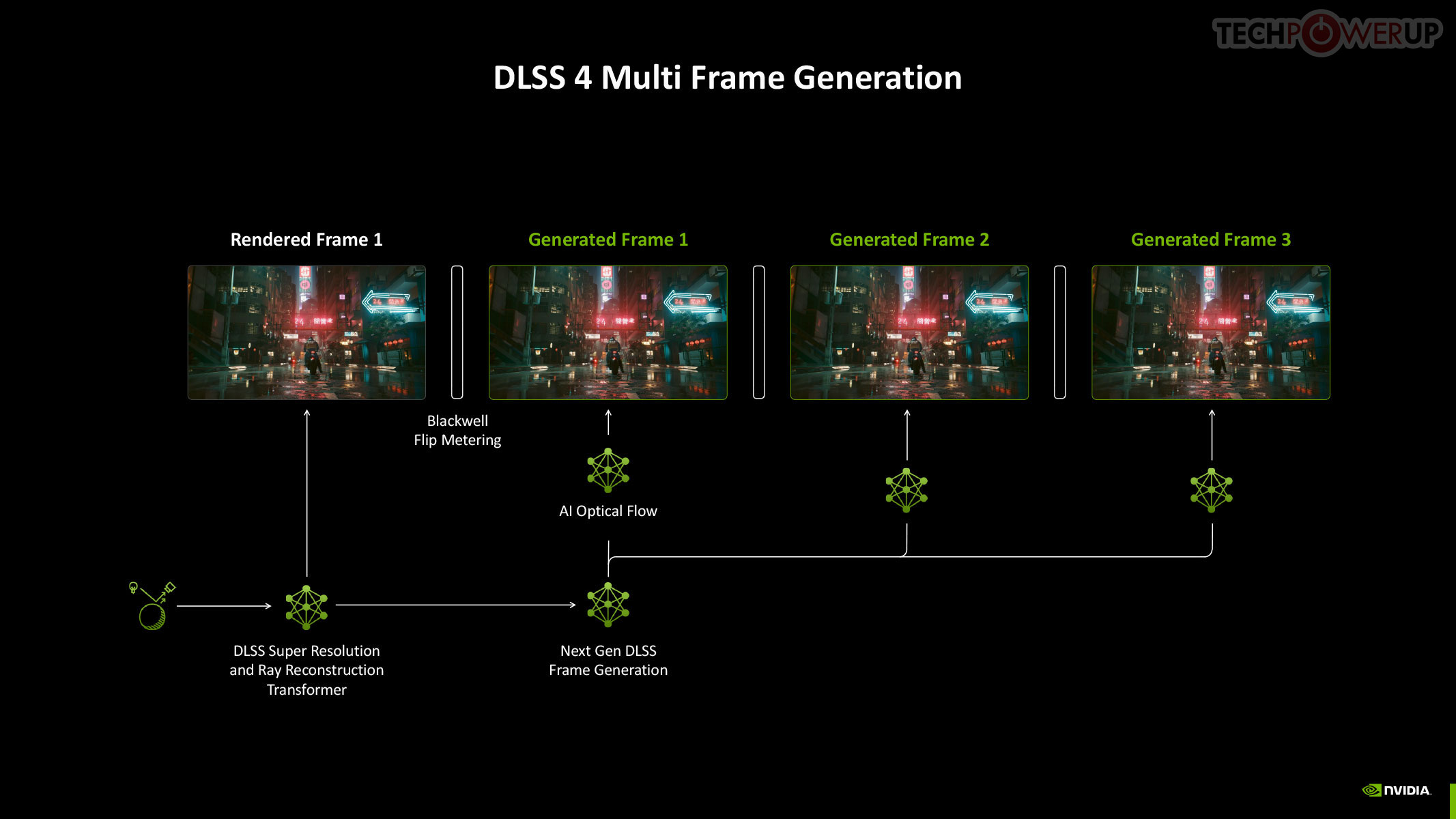
To understand Multi Frame Generation, you need to understand how DLSS Frame Generation, introduced with GeForce Ada, works. An Optical Flow Accelerator component gives the DLSS algorithm data to generate an entire frame using a neural network, using information from a previous rendered frame, effectively doubling frame rate. In Multi Frame Generation, AI takes over the functions of optical flow, to predict up to three frames following a conventionally rendered frame, effectively drawing four frames form the rendering effort of one.
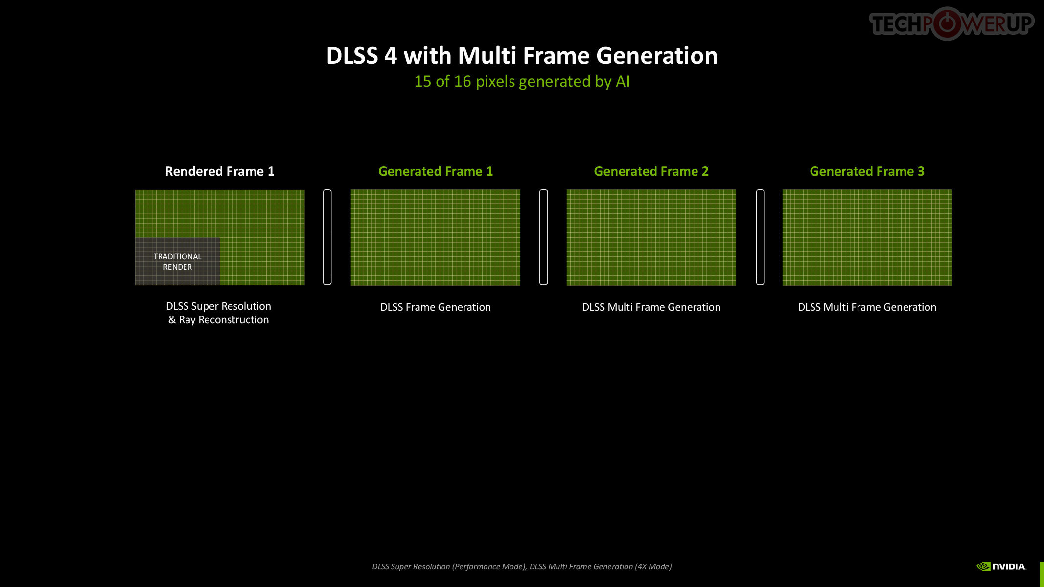
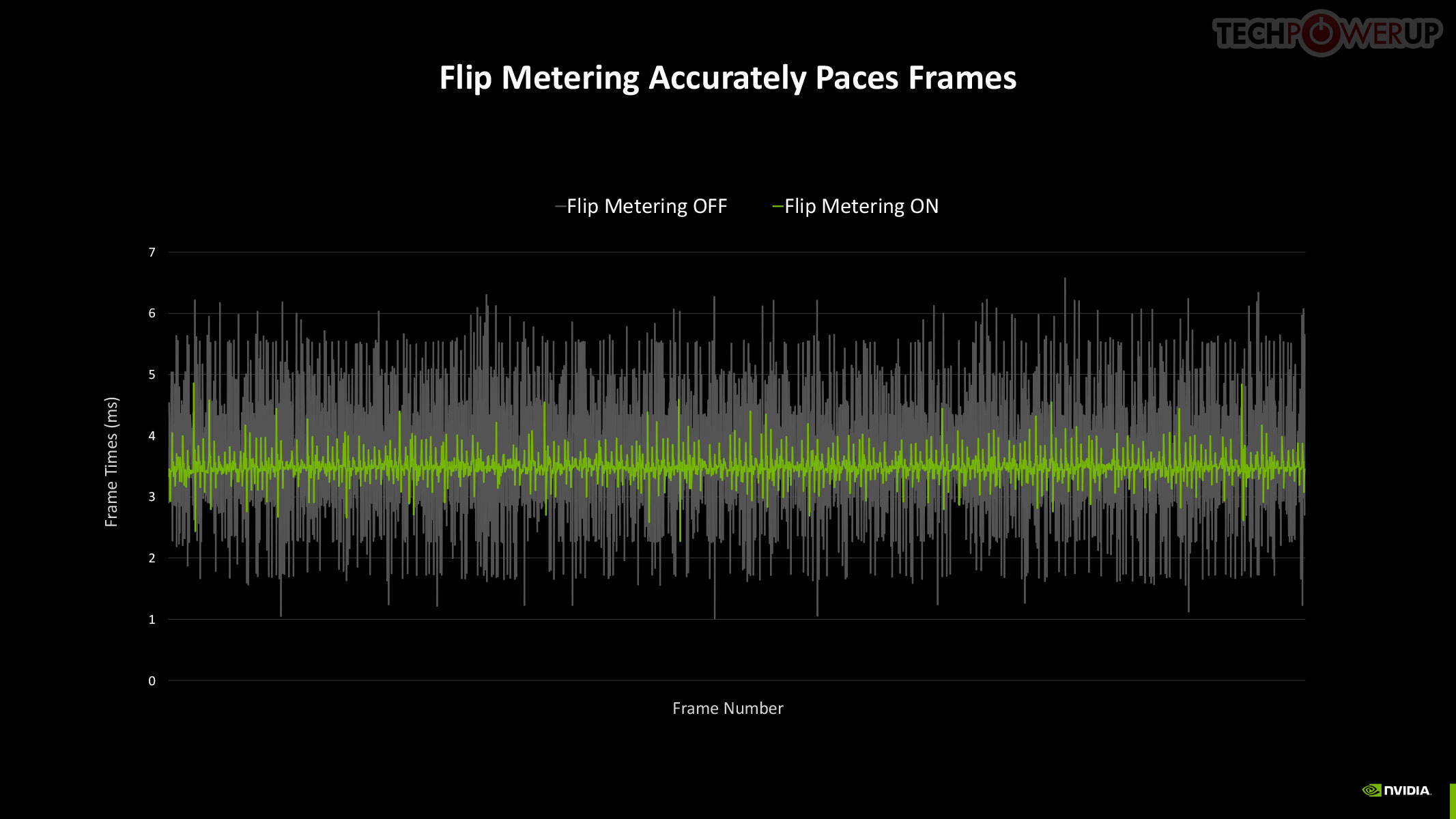
Now, assuming this rendered frame is a product of Super Resolution, with the maximum performance setting generating 4x the pixels from a single rendered pixel, you're looking at a possibility where the rendering effort of 1/4th a frame goes into drawing 4 frames, or 15 in every 16 pixels being generated entirely by DLSS. When generating so many frames, Frame Pacing becomes a problem—irregular frame intervals impact smoothness. DLSS 4 addresses these issues by using a dedicated hardware unit inside Blackwell, which takes care of flip metering, reducing frame display variability by 5-10x. The Display Engine of Blackwell contains the hardware for flip metering.
NVIDIA Reflex 2
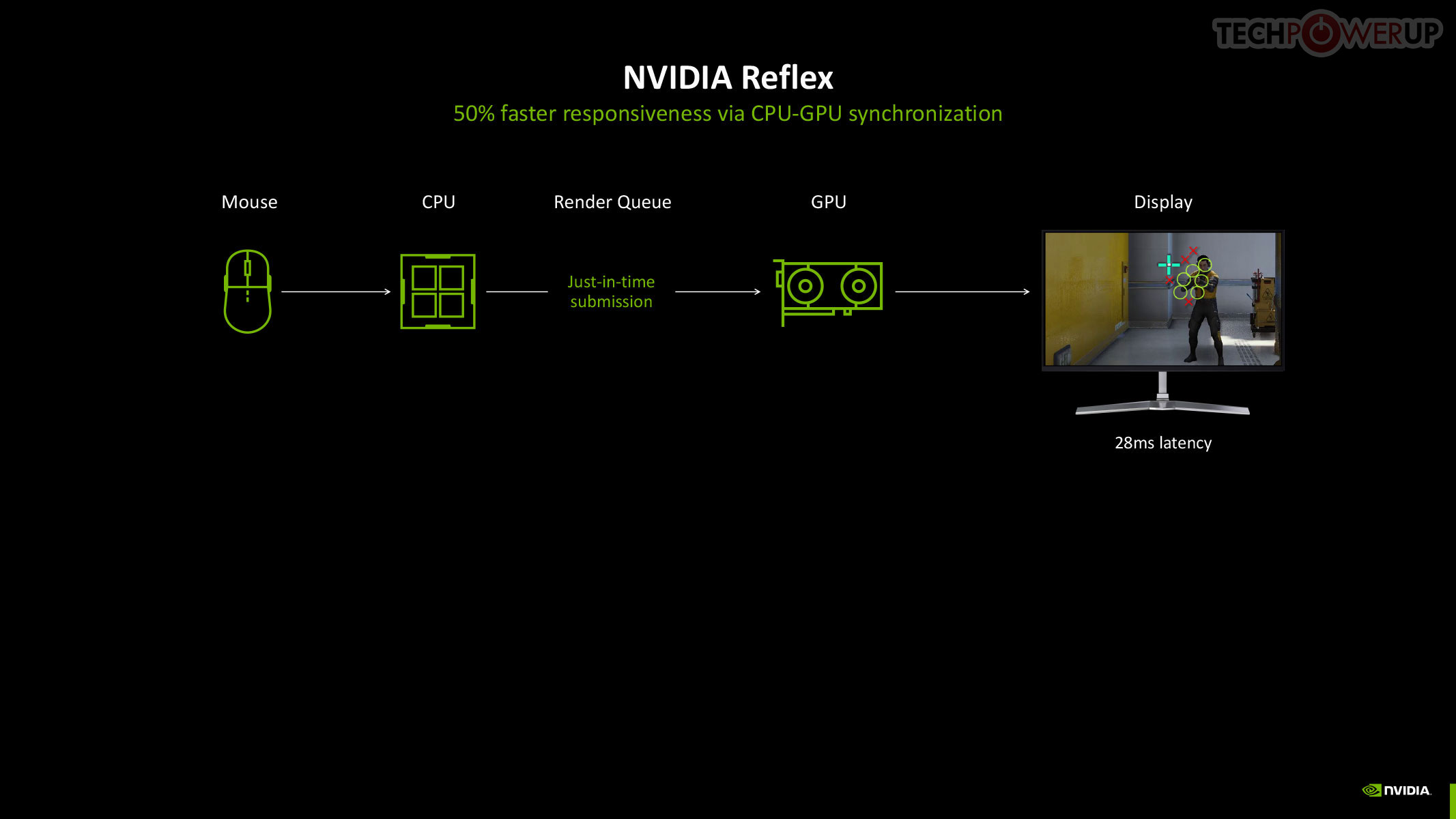
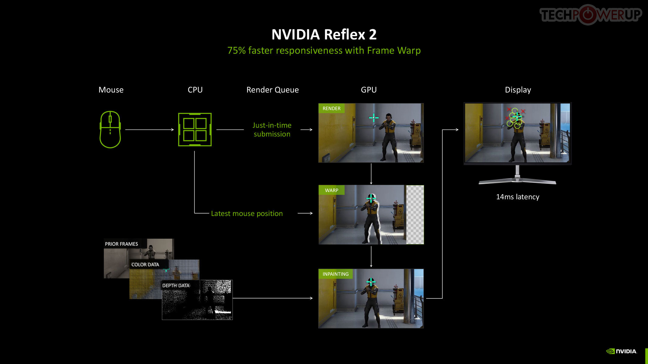
The original NVIDIA Reflex brought about a significant improvement to the responsiveness of maxed out graphics in competitive online gameplay, by compacting the rendering queue with the goal of reducing the whole system latency by up to 50%. Reflex is mandatory in DLSS 3 Frame Generation, given the latency cost imposed by the technology. Multi-frame generation calls for an equally savvy piece of technology, so we hence have Reflex 2. NVIDIA claims to have achieved a 75% reduction in latency with Frame Warp, which updates the camera (viewport) positions based on user inputs in real-time, and then uses temporal information to reconstruct the frame to display.
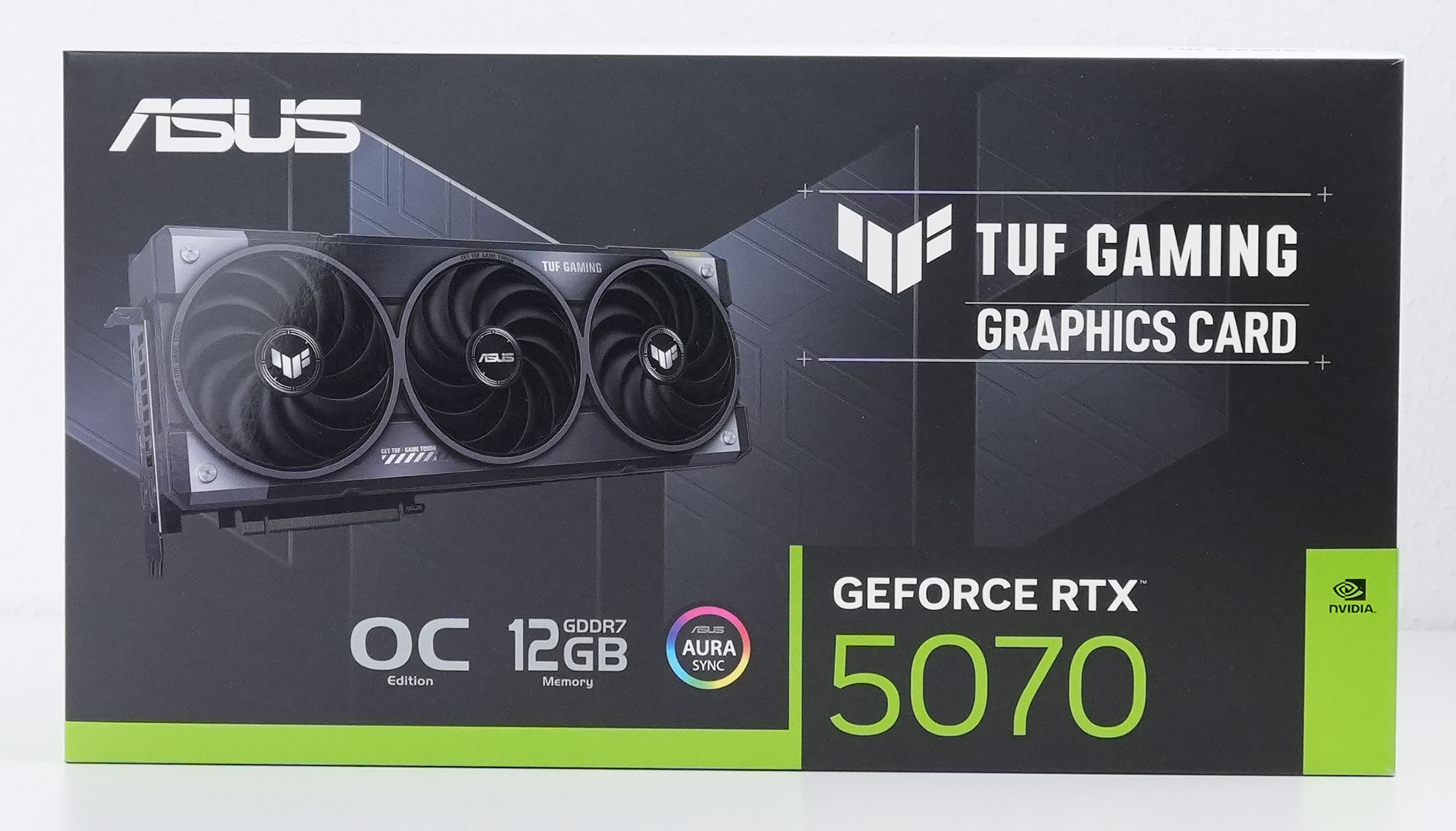
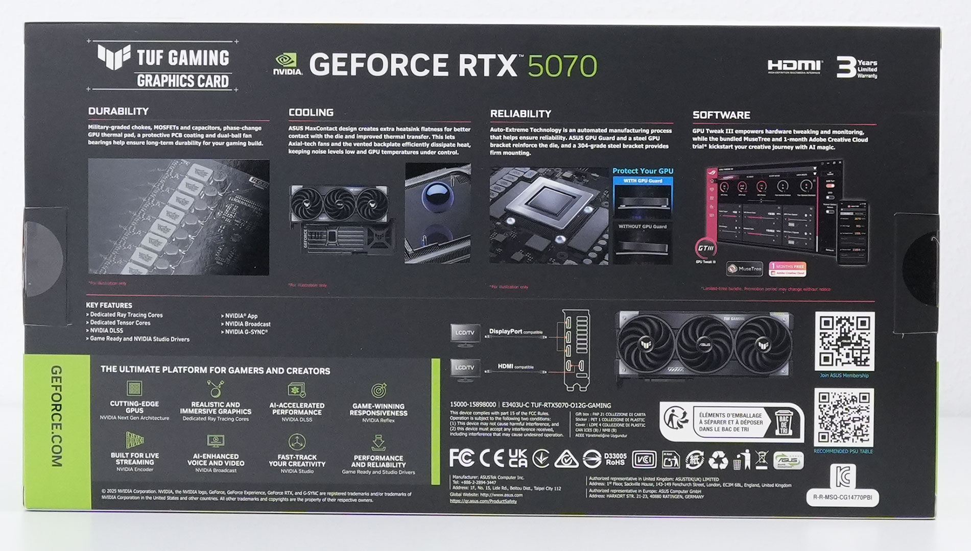
Packaging
The Card
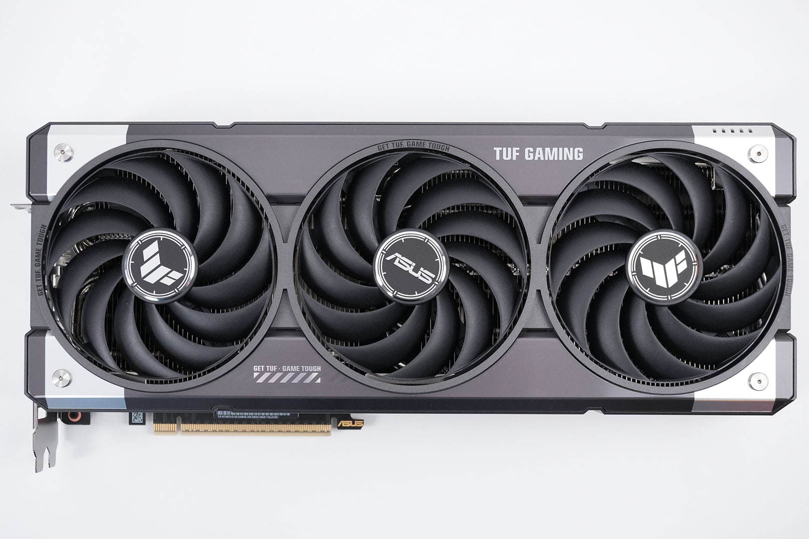
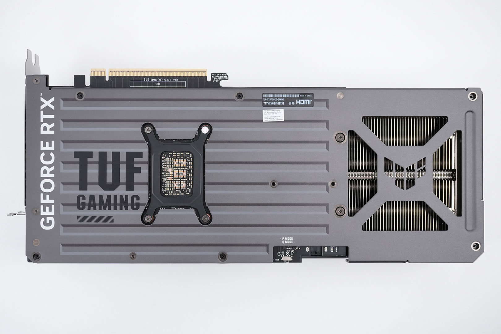
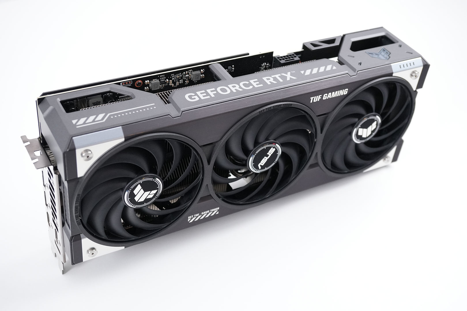
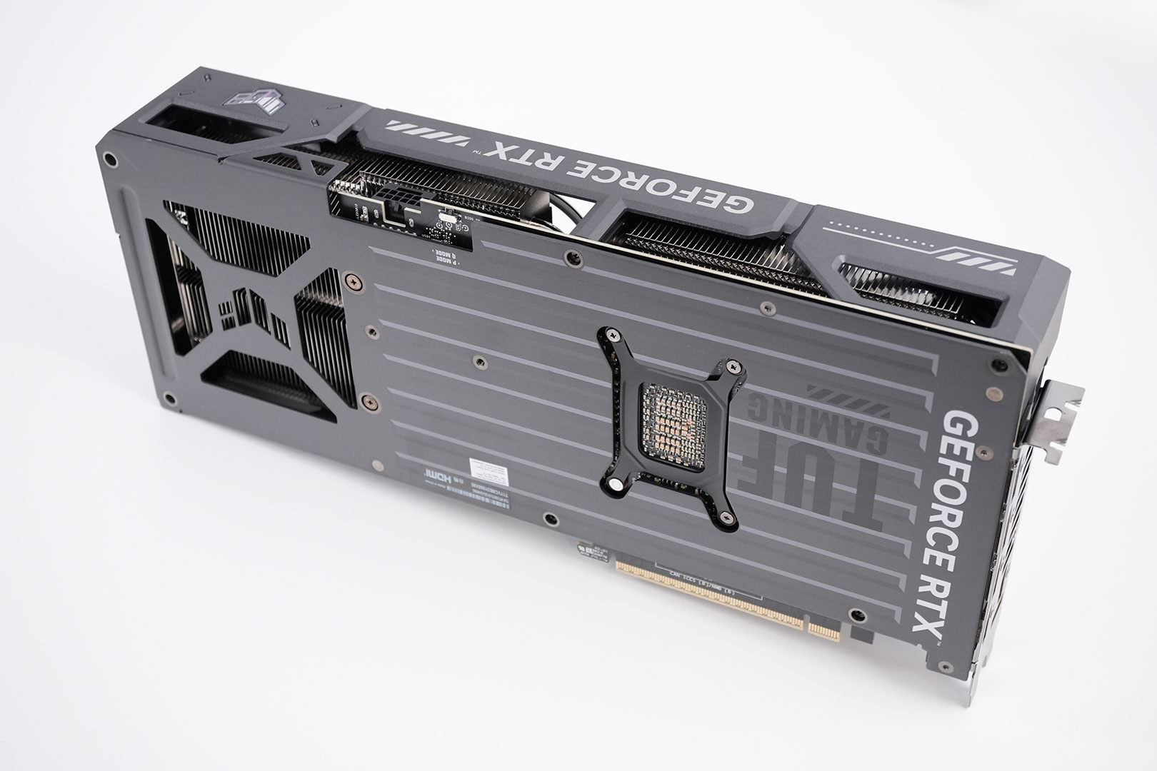
Visually, the ASUS RTX 5070 TUF OC follows the design theme of the company's previous TUF cards, and it also matches the RX 9070 TUF visuals exactly. On the back you get a high quality metal backplate with a cutout for air to flow through.
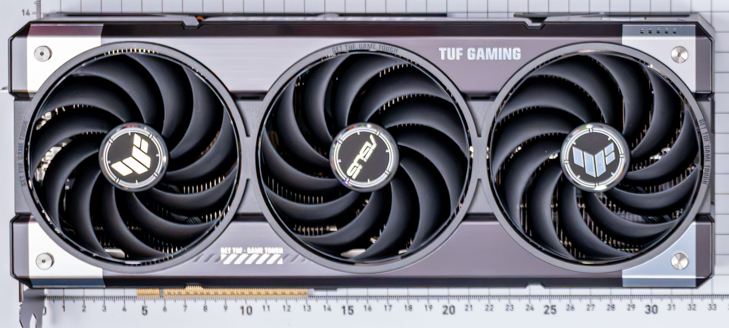
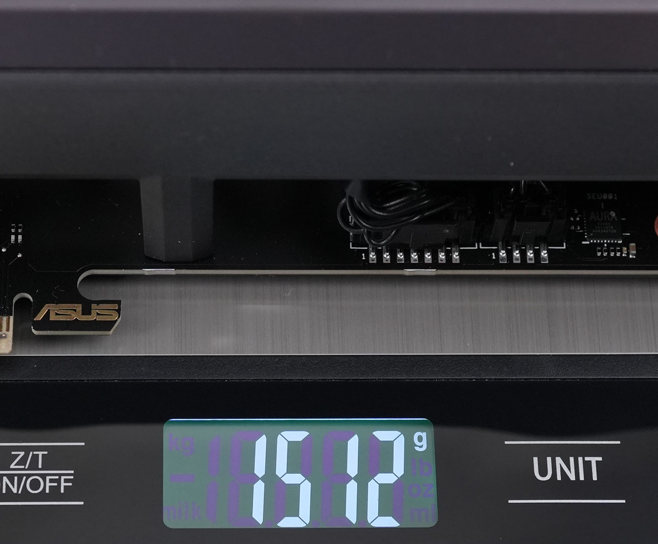
Dimensions of the card are 33.0 x 14.0 cm, and it weighs 1512 g.
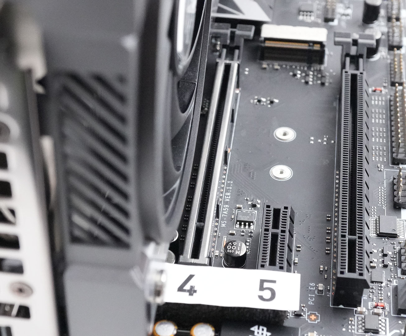
Installation requires three slots in your system. We measured the card's width to be 63 mm.
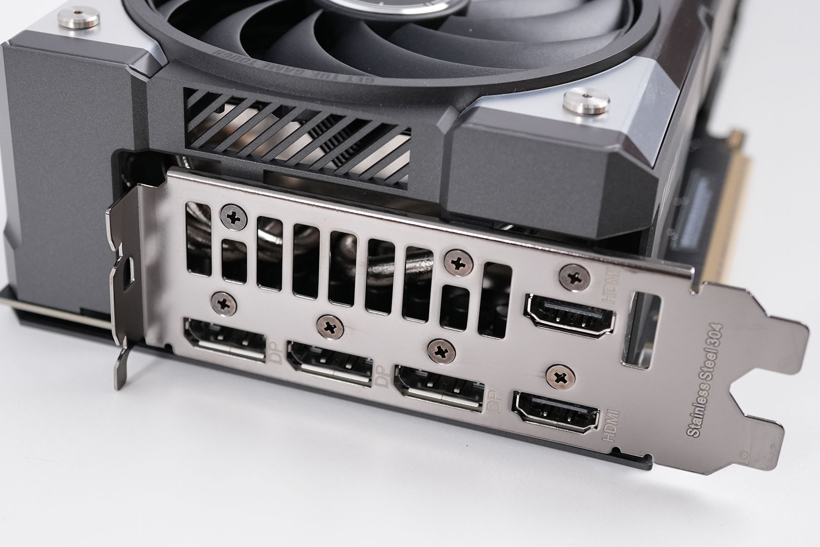
Display connectivity includes three standard DisplayPort 2.1b and two HDMI 2.1b.
Standard for all GeForce RTX 50-series Blackwell cards is a new display engine that supports three DisplayPort 2.1b outputs, each capable of UHBR20; and one HDMI 2.1a. Both interfaces support DSC (display stream compression). With DSC enabled, a single DisplayPort on this card can drive 4K 12-bit HDR at 480 Hz; or 8K 12-bit HDR at up to 165 Hz. The RTX 5070 features an updated media acceleration engine with support for 4:2:2 video formats, AV1 UHQ, and MV-HEVC. Unlike the bigger RTX 50 models, which have two, there is a single NVENC and NVDEC unit each.
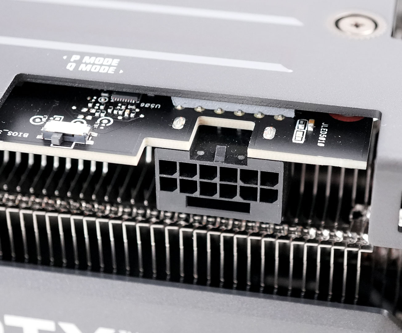
The card uses a single 16-pin connector, which allows a maximum power draw of 600 W, but the board power limit is set much lower of course.
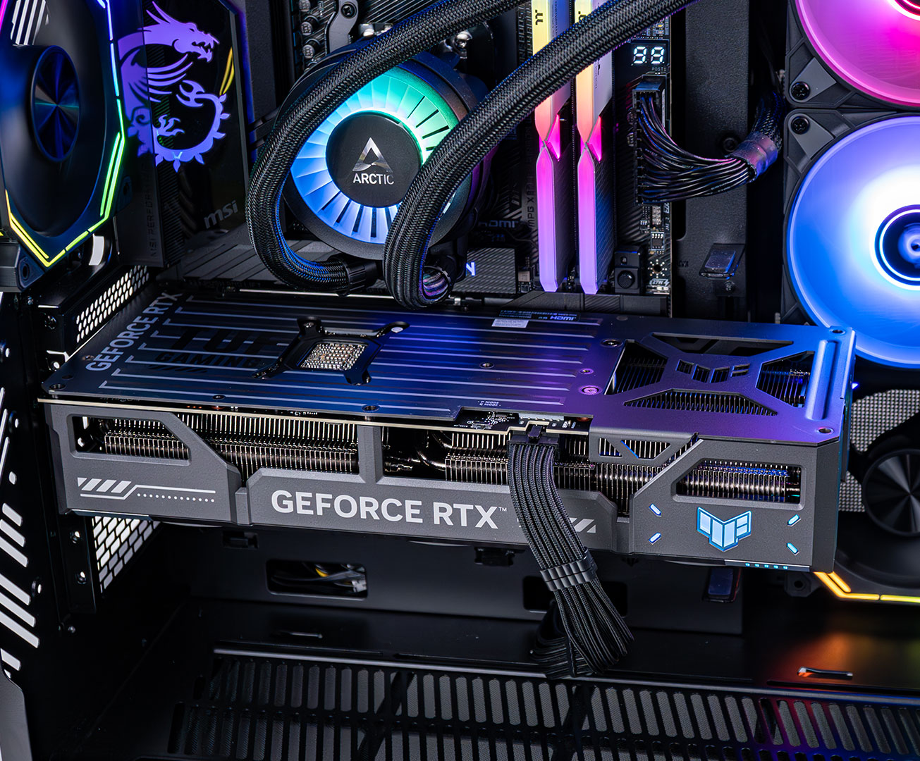
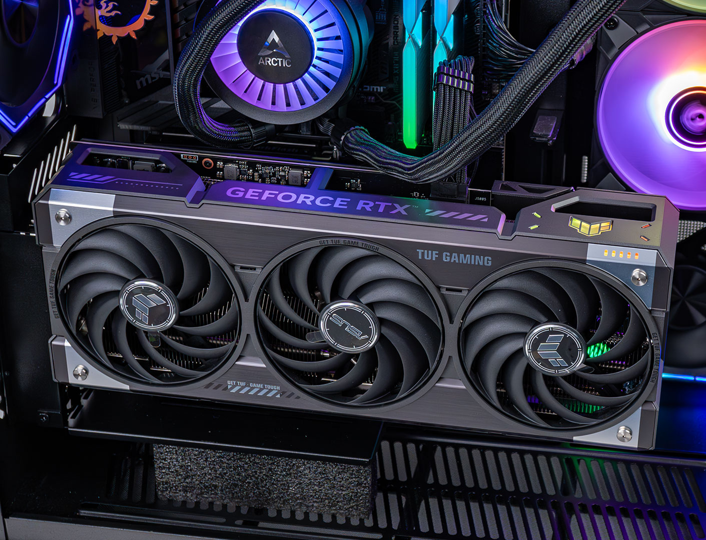
ASUS has installed an RGB lighting zone near the corner of the card.
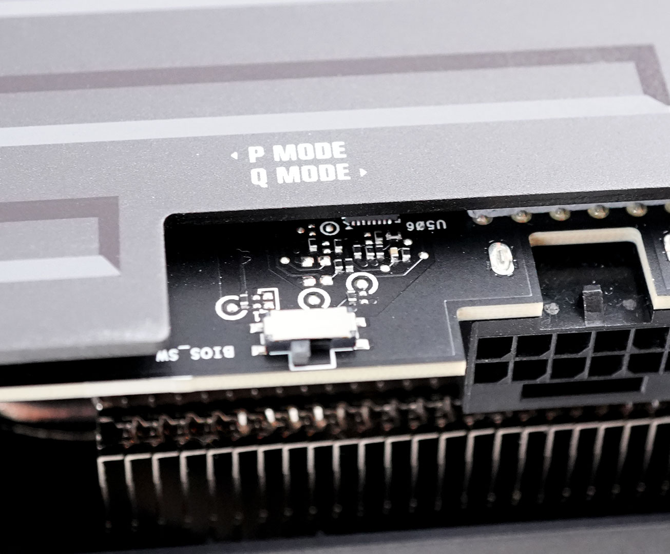
This BIOS switch lets you toggle between the default performance BIOS and an optional "quiet" BIOS.
Our Patreon Silver Supporters can read articles in single-page format.
Mar 25th, 2025 11:07 EDT
change timezone
Latest GPU Drivers
New Forum Posts
- RTX 5080 worth it over 5070 TI for 4k? (49)
- maxsun rx590* vbios (3)
- Is RX 9070 VRAM temperature regular value or hotspot? (188)
- Montech KING 95 - your opinions? (11)
- What local LLM-s you use? (142)
- What's your latest tech purchase? (23391)
- Lenovo ThinkPad L15 Gen 1 (AMD) - DRAM soldered? (8)
- Issues with RTX4090 FE waterblock (Bitspower) (2)
- Is Whatsapp backup broken for anyone else? (1)
- RX 9070 availability (228)
Popular Reviews
- Assassin's Creed Shadows Performance Benchmark Review - 30 GPUs Compared
- be quiet! Pure Rock Pro 3 Black Review
- ASUS ProArt X870E-Creator Wi-Fi Review
- ASRock Radeon RX 9070 XT Taichi OC Review - Excellent Cooling
- Sapphire Radeon RX 9070 XT Nitro+ Review - Beating NVIDIA
- ASUS GeForce RTX 5070 TUF OC Review
- AMD Ryzen 9 9950X3D Review - Great for Gaming and Productivity
- Quick Look: Jelly Key Mystic Snake Artisan Keycaps
- AMD Ryzen 7 9800X3D Review - The Best Gaming Processor
- XFX Radeon RX 9070 XT Mercury OC Magnetic Air Review
Controversial News Posts
- AMD RDNA 4 and Radeon RX 9070 Series Unveiled: $549 & $599 (260)
- AMD Mentions Sub-$700 Pricing for Radeon RX 9070 GPU Series, Looks Like NV Minus $50 Again (250)
- AMD Radeon RX 9070-series Pricing Leaks Courtesy of MicroCenter (158)
- MSI Doesn't Plan Radeon RX 9000 Series GPUs, Skips AMD RDNA 4 Generation Entirely (142)
- Microsoft Introduces Copilot for Gaming (123)
- AMD Radeon RX 9070 XT Reportedly Outperforms RTX 5080 Through Undervolting (118)
- NVIDIA Reportedly Prepares GeForce RTX 5060 and RTX 5060 Ti Unveil Tomorrow (115)
- Over 200,000 Sold Radeon RX 9070 and RX 9070 XT GPUs? AMD Says No Number was Given (100)