 17
17
ASUS Radeon RX 5600 XT TUF EVO Review
(17 Comments) »Introduction
Today, we have for review the ASUS Radeon RX 5600 XT TUF Gaming EVO graphics card positioned a notch below the ROG STRIX Radeon RX 5600 XT TOP OC graphics card we reviewed earlier. The TUF Gaming line of PC hardware and peripherals by ASUS represents durable, high cost to performance products targeted at gamers. The brand itself, though, has had some bad press in recent times over sub-optimal cooler designs that weren't well received by reviewers. Since then, the company worked extensively on improving the cooler and thermals of its Navi TUF Gaming graphics cards, and the culmination of that work is the TUF Gaming EVO board design, which made its debut with products based on the RX 5700 XT and RX 5700 series and has now been put onto the performance-segment RX 5600 XT. The important part in the nomenclature is the "EVO" as it denotes the new cooling solution.
AMD originally intended for the RX 5600 XT to take the performance crown unopposed by NVIDIA, as it designed the SKU to outclass the entire GeForce 16-series. With ray-tracing hardware off the table, the playing field was supposed to be level between AMD and NVIDIA; that is, until NVIDIA pulled a last-minute rabbit out of its hats with a price cut down to $299 for the GeForce RTX 2060. AMD scrambled to revise the specifications of the RX 5600 XT by increasing clock speeds and memory bandwidth in a bid to compete with the RTX 2060. Since products with the original specifications were already in circulation, the update in specifications was sloppily put out through video BIOS updates targeting only those cards that shipped with VRM and memory chips capable of the new specifications. The ASUS TUF Gaming EVO was conceived after this mess and yet only partially implements these. The default memory speed of the card is 12 Gbps, or 1500 MHz, with ASUS providing a BIOS update on their website to 14 Gbps, or 1750 MHz, to match other high-end Radeon RX 5600 XT graphics cards.

Based on the same 7 nm "Navi 10" silicon as the RX 5700 series, the Radeon RX 5600 XT is configured with 2,304 stream processors spread across 36 RDNA compute units—same as the RX 5700, but with the memory amount slashed by a third, down to 6 GB, along with the memory bus, down to 192-bit GDDR6. AMD also tinkered with the GPU clock speeds a bit. The idea behind the RX 5600 XT is to dominate the sub-$300 graphics card market, providing 1080p gaming at frame rates of around 90 FPS, or even 1440p with reasonable frame rates.
The ASUS Radeon RX 5600 XT TUF EVO in this review is based on the revised TUF Gaming EVO board design we mentioned earlier. This design sees an overhaul of the heatsink underneath the cooler shroud to make it vent out heat better, and the inclusion of ASUS's premium Axial Tech fans that feature webbed impellers that guide all of their airflow axially (none bleeding laterally). The board draws power from a single 8-pin PCIe power connector and includes a few premium touches, such as a metal backplate and an ARGB embellishment. ASUS is pricing the card at $320, a $40 premium over the $280 AMD baseline price.
| Price | Shader Units | ROPs | Core Clock | Boost Clock | Memory Clock | GPU | Transistors | Memory | |
|---|---|---|---|---|---|---|---|---|---|
| GTX 1070 | $300 | 1920 | 64 | 1506 MHz | 1683 MHz | 2002 MHz | GP104 | 7200M | 8 GB, GDDR5, 256-bit |
| RX Vega 56 | $260 | 3584 | 64 | 1156 MHz | 1471 MHz | 800 MHz | Vega 10 | 12500M | 8 GB, HBM2, 2048-bit |
| GTX 1660 Super | $230 | 1408 | 48 | 1530 MHz | 1785 MHz | 1750 MHz | TU116 | 6600M | 6 GB, GDDR6, 192-bit |
| GTX 1660 Ti | $270 | 1536 | 48 | 1500 MHz | 1770 MHz | 1500 MHz | TU116 | 6600M | 6 GB, GDDR6, 192-bit |
| GTX 1070 Ti | $450 | 2432 | 64 | 1607 MHz | 1683 MHz | 2000 MHz | GP104 | 7200M | 8 GB, GDDR5, 256-bit |
| RX 5600 XT | $270 | 2304 | 64 | 1375 MHz | 1560 MHz | 1500 MHz | Navi 10 | 10300M | 6 GB, GDDR6, 192-bit |
| ASUS RX 5600 XT TUF EVO | $320 | 2304 | 64 | 1615 MHz | 1750 MHz | 1750 MHz | Navi 10 | 10300M | 6 GB, GDDR6, 192-bit |
| RTX 2060 | $300 | 1920 | 48 | 1365 MHz | 1680 MHz | 1750 MHz | TU106 | 10800M | 6 GB, GDDR6, 192-bit |
| RX 5700 | $320 | 2304 | 64 | 1465 MHz | 1625 MHz | 1750 MHz | Navi 10 | 10300M | 8 GB, GDDR6, 256-bit |
| GTX 1080 | $500 | 2560 | 64 | 1607 MHz | 1733 MHz | 1251 MHz | GP104 | 7200M | 8 GB, GDDR5X, 256-bit |
| RTX 2060 Super | $400 | 2176 | 64 | 1470 MHz | 1650 MHz | 1750 MHz | TU106 | 10800M | 8 GB, GDDR6, 256-bit |
| RX Vega 64 | $390 | 4096 | 64 | 1247 MHz | 1546 MHz | 953 MHz | Vega 10 | 12500M | 8 GB, HBM2, 2048-bit |
Packaging


The Card


For their TUF series, ASUS created a new design identity. The card uses black and various shades of gray. Note how the center fan is smaller than the surrounding ones—this is new on the EVO version. A metal backplate in matching colors is included, too.

Dimensions of the card are 28 x 13 cm.


Installation requires three slots in your system.

Display connectivity options include three standard DisplayPort 1.4a and an HDMI 2.0b.

The board uses one 8-pin power connector. This input configuration is specified for up to 225 watts of power draw.

AMD's Navi generation of GPUs no longer supports CrossFire. DirectX 12 does include its own set of multi-GPU capabilities, but implementation requires game developers to put serious development time into a feature only a tiny fraction of their customers might ever use.
Disassembly


As mentioned in the introduction, ASUS had some issues with the initial batch of TUF cards, which caused public outcry from consumers and reviewers. We are testing the fixed version, which has upgraded fans with axial tech to direct the airflow through the fins. Also note how the fan impellers are surrounded by a plastic ring to ensure no air can escape horizontally. The outer fans are 90 mm in diameter, and the center fan is 80 mm across.
The cooling assembly is 100% identical to the one used for the Radeon RX 5700 XT TUF EVO.


Once the cooling assembly is removed, you get access to the heatsink. It uses five heatpipes and a large array of fins to keep the card cool. This heatsink provides cooling for the GPU, memory chips, and VRM circuitry. Do note that the memory chips are cooled by a plate that is bolted to the heatsink—it is not part of it. This means heat transfer is slightly reduced, but still much better than on the original TUF, which just had a thin metal heatspreader on the memory that did not connect with the main heatsink at all.

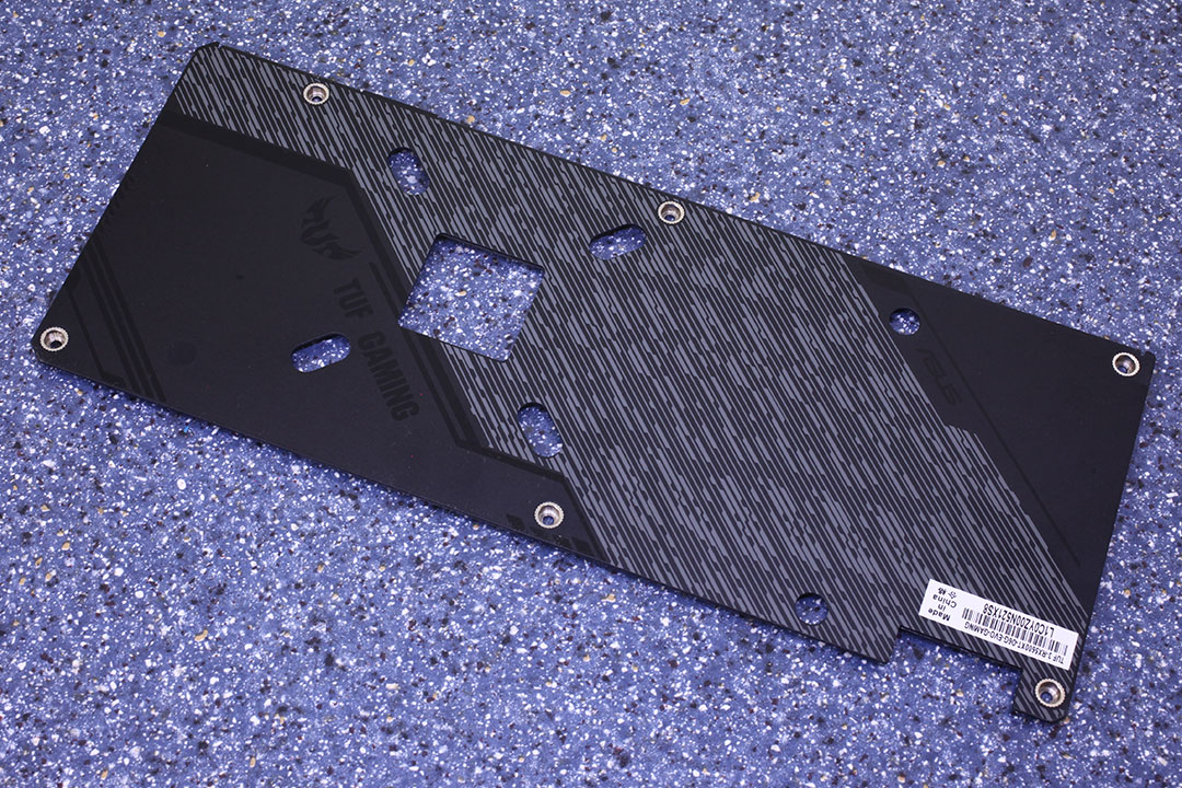
The backplate is made out of metal to protect the card against damage during installation and handling. There are some thermal pads to pick up a little bit of heat from the other side of the memory chips.
High-resolution PCB Pictures
These pictures are for the convenience of volt modders and people who would like to see all the finer details on the PCB. Feel free to link back to us and use these in your articles or forum posts.

High-res versions are also available (front, back).
Circuit Board (PCB) Analysis


The GPU VRM is 7+1-phase, controlled by an International Rectifier IR35217 controller, which is among the best controllers available on the market.

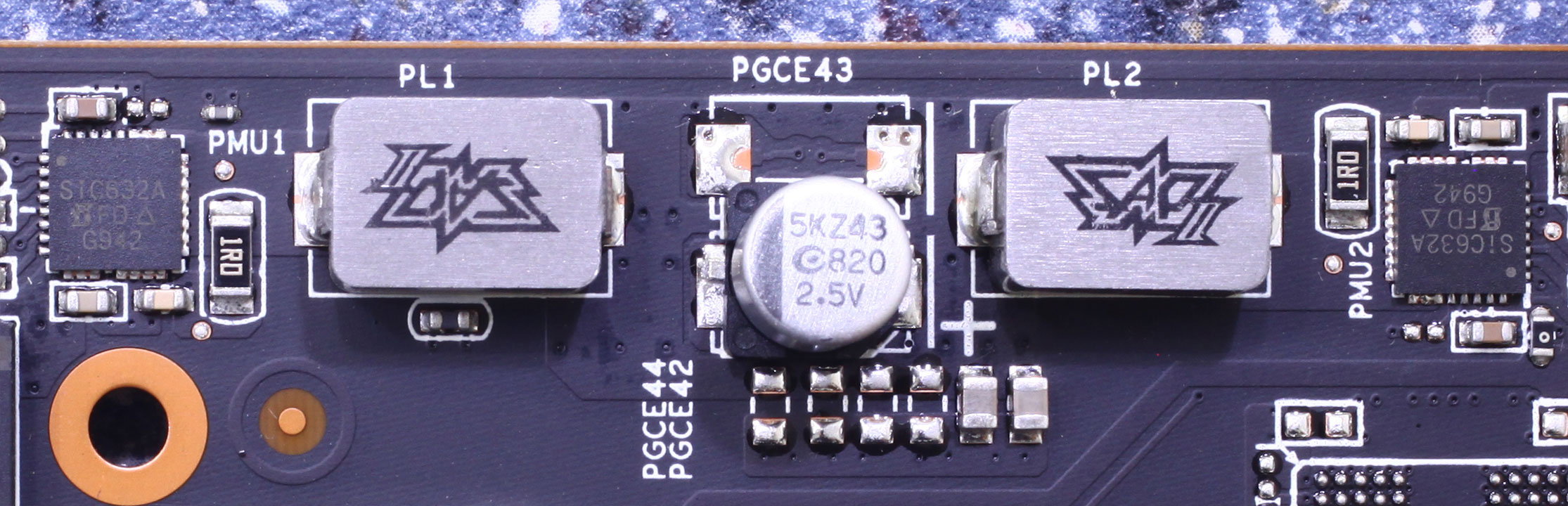
Memory voltage uses a two-phase design and is generated by an International Rectifier IR3567B controller.

The GDDR6 memory chips are made by Micron and carry the model number D9WCW, which decodes to MT61K256M32JE-14:A. They are specified to run at 1750 MHz (14 Gbps GDDR6 effective).

AMD's Navi 10 graphics processor is their first chip to use the new RDNA architecture. It is produced on a 7 nanometer process at TSMC, Taiwan and has a transistor count of 10.3 billion with a die size of 251 mm².
Our Patreon Silver Supporters can read articles in single-page format.
Apr 11th, 2025 16:25 EDT
change timezone
Latest GPU Drivers
New Forum Posts
- Post your cooling. (225)
- TPU's Nostalgic Hardware Club (20231)
- What's your latest tech purchase? (23520)
- Is there potential for AMD to change the world with this x3D technology combined with gallium cooling techniques? (3)
- Soyo RX 580 8G 2048SP problem (1)
- Bios RX 570 (13)
- I need help finding the correct vBIOS for my Chinese graphics card. It's an RX 580 (5)
- (Some of) What I'd like to See From a Final Fantasy IX Remake (23)
- Asus X670E Crosshair Crashes (17)
- Deal or no Deal Threadripper WX? (3)
Popular Reviews
- The Last Of Us Part 2 Performance Benchmark Review - 30 GPUs Compared
- Thermaltake TR100 Review
- ASRock Z890 Taichi OCF Review
- Zotac GeForce RTX 5070 Ti Amp Extreme Review
- Sapphire Radeon RX 9070 XT Pulse Review
- Sapphire Radeon RX 9070 XT Nitro+ Review - Beating NVIDIA
- Acer Predator GM9000 2 TB Review
- Upcoming Hardware Launches 2025 (Updated Apr 2025)
- PowerColor Radeon RX 9070 Hellhound Review
- TerraMaster F8 SSD Plus Review - Compact and quiet
Controversial News Posts
- NVIDIA GeForce RTX 5060 Ti 16 GB SKU Likely Launching at $499, According to Supply Chain Leak (180)
- MSI Doesn't Plan Radeon RX 9000 Series GPUs, Skips AMD RDNA 4 Generation Entirely (146)
- Microsoft Introduces Copilot for Gaming (124)
- AMD Radeon RX 9070 XT Reportedly Outperforms RTX 5080 Through Undervolting (119)
- NVIDIA Reportedly Prepares GeForce RTX 5060 and RTX 5060 Ti Unveil Tomorrow (115)
- NVIDIA Sends MSRP Numbers to Partners: GeForce RTX 5060 Ti 8 GB at $379, RTX 5060 Ti 16 GB at $429 (111)
- Nintendo Confirms That Switch 2 Joy-Cons Will Not Utilize Hall Effect Stick Technology (104)
- Over 200,000 Sold Radeon RX 9070 and RX 9070 XT GPUs? AMD Says No Number was Given (100)