 19
19
EVGA GeForce GTX 1660 Super SC Ultra Review
Test Setup »High-resolution PCB Pictures
These pictures are for the convenience of volt modders and people who would like to see all the finer details on the PCB. Feel free to link back to us and use these in your articles or forum posts.

High-res versions are also available (front, back).
Circuit Board (PCB) Analysis
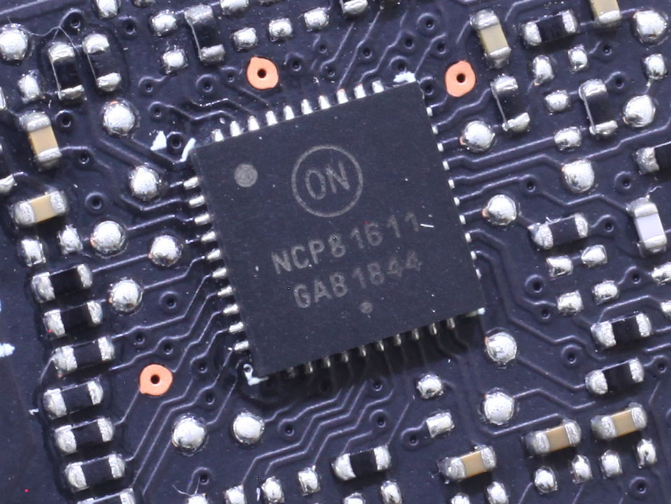
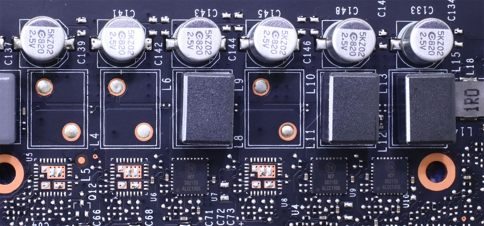
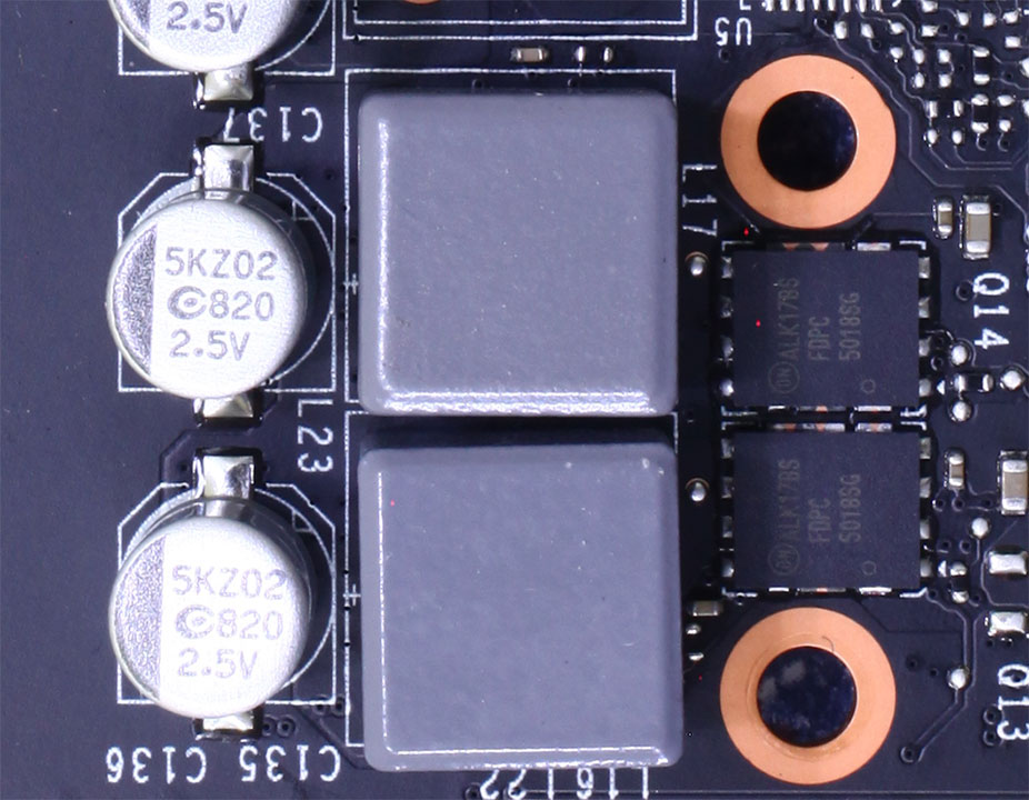
EVGA is using a very simple 3-phase VRM to power the GPU, controlled by an On Semi NCP81611 controller. These are direct phases without any doubling (which the PCB has provision for). Interestingly, EVGA chose premium On Semi DrMOS components, which are passively cooled under the cooler's airflow.
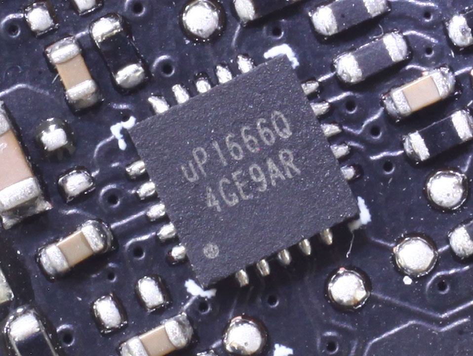
The memory VRM is 2-phase and managed by a UPI uP1666Q controller.
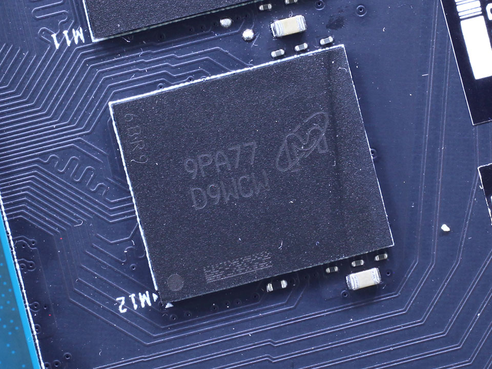
The GDDR6 memory chips are made by Micron and carry the model number D9WCW, which decodes to MT61K256M32JE-14:A. They are specified to run at 1750 MHz (14 Gbps GDDR6 effective).

NVIDIA's TU116 graphics processor is the company's first chip with the Turing architecture that does not include Tensor cores or ray-tracing acceleration. It is produced on a 12 nm process at TSMC, Taiwan and has a transistor count of 6.6 billion with a die size of 284 mm².
May 4th, 2025 17:06 EDT
change timezone
Latest GPU Drivers
New Forum Posts
- 12600KF high latency (22)
- Are the 8 GB cards worth it? (830)
- PSU chirping sound (13)
- What are you playing? (23544)
- Half Life 3 soon ? (6)
- Choosing an Internal HDD (59)
- 5070 Ti power limit questions (83)
- Free Games Thread (4663)
- type 5 miccro-fit sata cables (8)
- Vertical mice in gaming (7)
Popular Reviews
- Clair Obscur: Expedition 33 Performance Benchmark Review - 33 GPUs Tested
- ASUS ROG Maximus Z890 Hero Review
- ASUS Radeon RX 9070 XT TUF OC Review
- Montech HS02 PRO Review
- NVIDIA GeForce RTX 5060 Ti 8 GB Review - So Many Compromises
- ASUS GeForce RTX 5090 Astral Liquid OC Review - The Most Expensive GPU I've Ever Tested
- Seasonic Vertex GX 850 W Review
- Upcoming Hardware Launches 2025 (Updated Apr 2025)
- ASRock Radeon RX 9070 XT Taichi OC Review - Excellent Cooling
- Sapphire Radeon RX 9070 XT Nitro+ Review - Beating NVIDIA
Controversial News Posts
- AMD Radeon RX 9060 XT to Roll Out 8 GB GDDR6 Edition, Despite Rumors (129)
- NVIDIA Sends MSRP Numbers to Partners: GeForce RTX 5060 Ti 8 GB at $379, RTX 5060 Ti 16 GB at $429 (128)
- NVIDIA Launches GeForce RTX 5060 Series, Beginning with RTX 5060 Ti This Week (115)
- Nintendo Confirms That Switch 2 Joy-Cons Will Not Utilize Hall Effect Stick Technology (105)
- NVIDIA PhysX and Flow Made Fully Open-Source (95)
- Sony Increases the PS5 Pricing in EMEA and ANZ by Around 25 Percent (84)
- Parts of NVIDIA GeForce RTX 50 Series GPU PCB Reach Over 100°C: Report (78)
- Intel "Bartlett Lake-S" Gaming CPU is Possible, More Hints Appear for a 12 P-Core SKU (77)