 17
17
EVGA GTX 1660 XC Ultra 6 GB Review
Test Setup »High-resolution PCB Pictures
These pictures are for the convenience of volt-modders and those who would like to see all the finer details on the PCB. Feel free to link back to us and use them in your articles or forum posts.
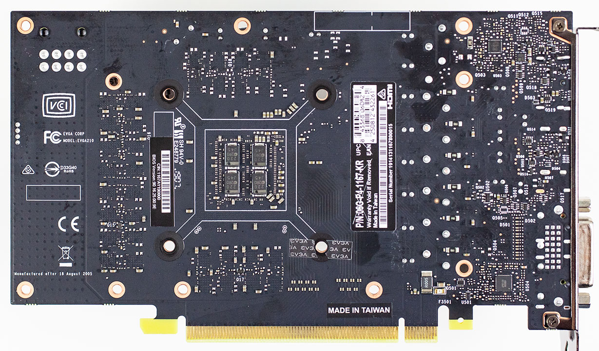
High-res versions are also available (front, back).
Circuit Board (PCB) Analysis
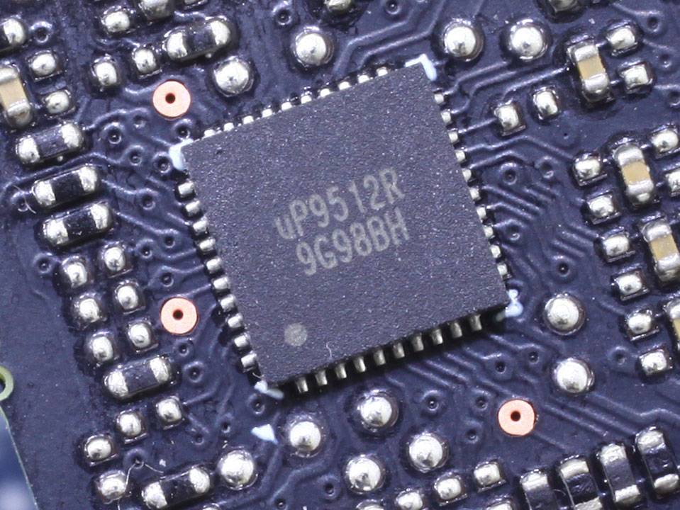
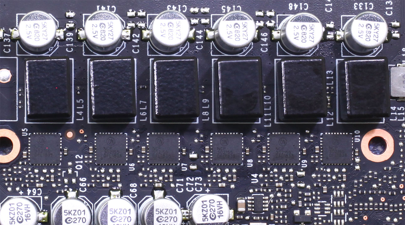
The GPU VRM is 6-phase, controlled by a UPI uP9512R controller.
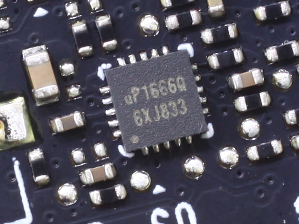
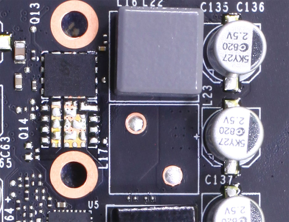
The memory VRM is 1-phase, managed by a UPI uP1666Q.
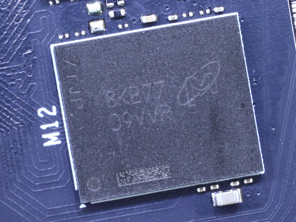
The GDDR5 memory chips are made by Micron and carry the model number D9VVR, which decodes to MT51J256M32HF-80:B. They are specified to run at 2000 MHz (8 Gbps GDDR5 effective).
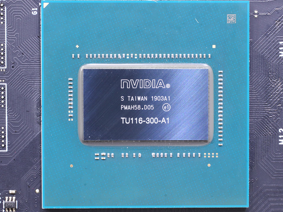
NVIDIA's TU116 graphics processor is the company's first chip with the Turing architecture that does not include Tensor cores or ray-tracing acceleration. It is produced on a 12 nm process at TSMC, Taiwan and has a transistor count of 6.6 billion with a die size of 284 mm².
Unlike previous Turing GPUs, which separated "non-OC" chips and chips for factory overclocking by adding an "A" designation on the chip variant, all TU116 chips on the GTX 1660 Ti are TU116-400 (without the A) and can be used for OC cards.
Jan 24th, 2025 03:46 EST
change timezone
Latest GPU Drivers
New Forum Posts
- I find the lack of Battle Mage owners threads disturbing. My Onix Odyssey B580 arrived. (1)
- 5090 AIB Clocks (2)
- TPU's Nostalgic Hardware Club (19833)
- Client experiences access and ping dropout on local IP (2)
- B580 tanks performance with low end CPUs (147)
- New to building and need mobo advice (0)
- Ryzen 7600 ram 64gb vs 2 /4 channel,vs higher speed (80)
- Flex firmware flashing (1)
- for those who think 12gb vram can max out everything (122)
- CUDIMM OC Progress (0)
Popular Reviews
- NVIDIA GeForce RTX 5090 Founders Edition Review - The New Flagship
- NVIDIA GeForce RTX 5090 Founders Edition Unboxing
- NVIDIA GeForce RTX 5090 PCI-Express Scaling
- Alphacool Apex 1 CPU Water Block Review - Performance King!
- NZXT C1500 Review
- Pwnage StormBreaker Max CF Review
- PowerColor Alphyn AH10 Review
- AMD Ryzen 7 9800X3D Review - The Best Gaming Processor
- Montech Heritage Pro Review - The Leather Case
- NVIDIA GeForce RTX 50 Technical Deep Dive
Controversial News Posts
- NVIDIA 2025 International CES Keynote: Liveblog (470)
- AMD Debuts Radeon RX 9070 XT and RX 9070 Powered by RDNA 4, and FSR 4 (349)
- AMD Radeon RX 9070 XT & RX 9070 Custom Models In Stock at European Stores (226)
- NVIDIA GeForce RTX 5090 Features 575 W TDP, RTX 5080 Carries 360 W TDP (217)
- AMD Radeon RX 9070 XT Alleged Benchmark Leaks, Underwhelming Performance (205)
- AMD is Taking Time with Radeon RX 9000 to Optimize Software and FSR 4 (197)
- AMD's Radeon RX 9070 Launch Faces Pricing Hurdles (175)
- Potential RTX 5090 and RTX 5080 Pricing in China Leaks (173)