 21
21
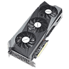
Gigabyte GeForce RTX 3070 Ti Gaming OC Review
Test Setup »High-resolution PCB Pictures
These pictures are for the convenience of volt modders and people who would like to see all the finer details on the PCB. Feel free to link back to us and use these in your articles, videos or forum posts.

High-res versions are also available (front, back).
Circuit Board (PCB) Analysis
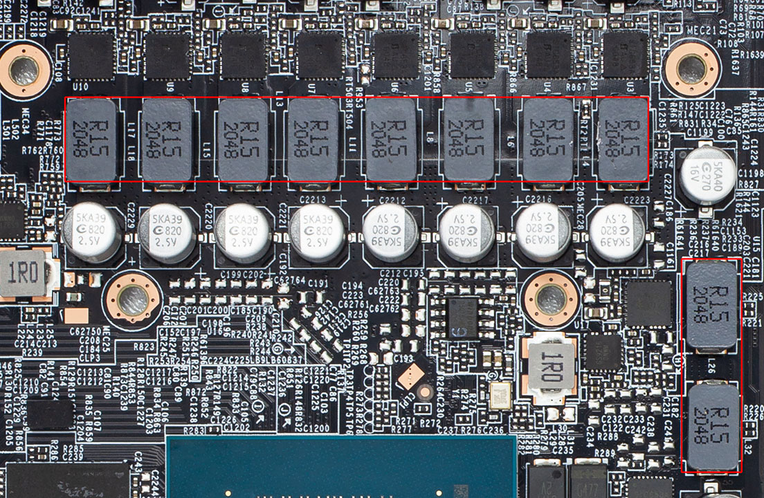
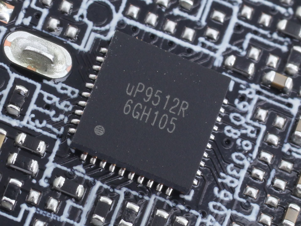
The GPU VRM is 10-phase, controlled by a UPI uP9512R voltage controller.
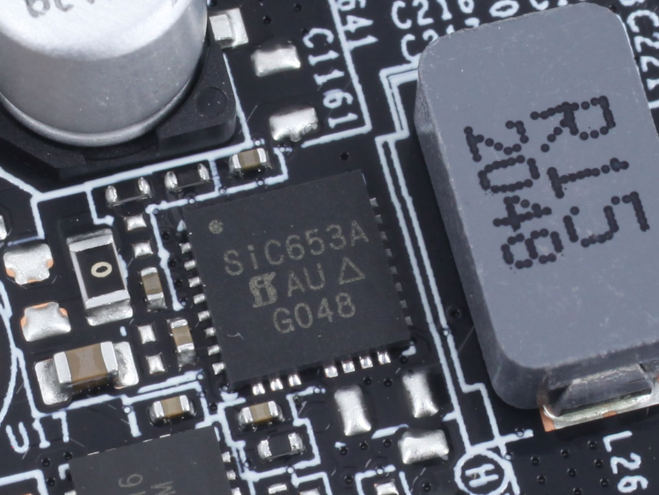
The GPU VRM uses Vishay SiC653 DrMOS components rated for 50 A.
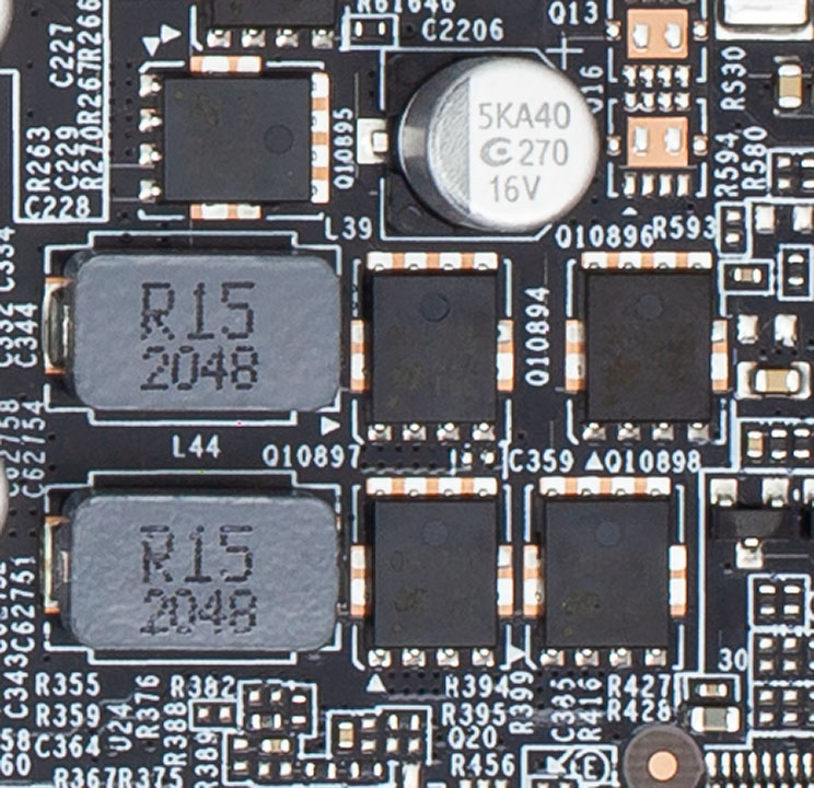
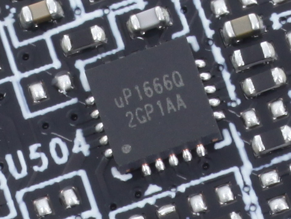
Memory is a two-phase design controlled by a uPI uP1666Q controller.
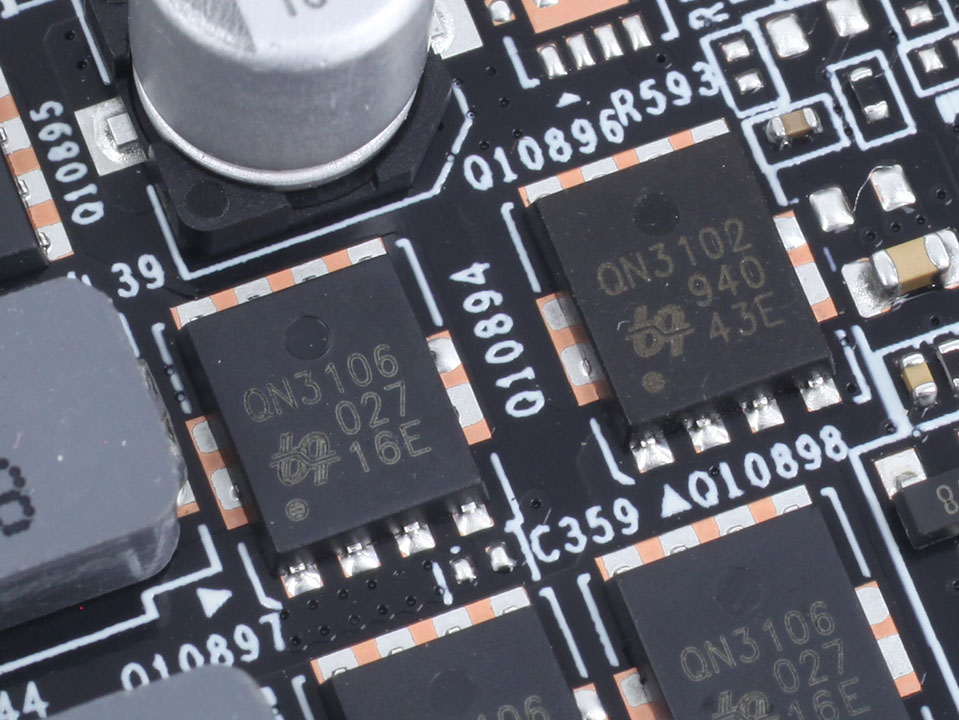
Each memory phase uses a combo of uPI QN3106 and QN3102 MOSFETs.
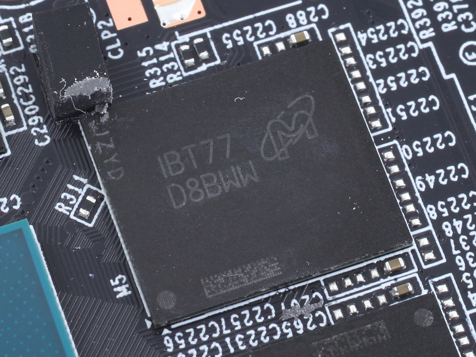
The GDDR6X memory chips are made by Micron and carry the model number D8BWW, which decodes to MT61K256M32JE-19G:T. They are specified to run at 1188 MHz (19 Gbps GDDR6X effective).
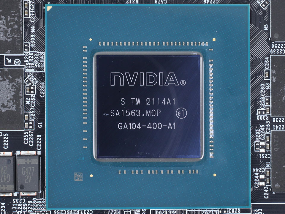
NVIDIA's GA104 graphics processor is the company's third Ampere architecture chip, the second one targeted at GeForce gamers. It is produced on a 8 nanometer process at Samsung and has a transistor count of 17.4 billion with a die size of 392 mm².
Mar 3rd, 2025 08:59 EST
change timezone
Latest GPU Drivers
New Forum Posts
- Was pentium 4 an over engineered CPU? (42)
- Trying to run 4k 144hz using 3070ti (19)
- Microcenter GPU Stock status (16)
- How many continuous hours will it last my mini pc if connected to the LiitoKala battery pack that I've found for a cheap price ? (45)
- question about blower fan gpu (20)
- Issues with clock speed not increasing (28)
- Recommended PhysX card for 5xxx series? [Is vRAM relevant?] (109)
- Help finding bios for rx 580 2048sp (11)
- Just a rant about AMD and their so-called "foolproofness" (126)
- Cooling problems persist on LGA1700 (22)
Popular Reviews
- AMD Radeon RX 9070 Series Technical Deep Dive
- be quiet! Pure Base 501 DX Review
- ASUS GeForce RTX 5070 Ti TUF OC Review
- AMD Ryzen 7 9800X3D Review - The Best Gaming Processor
- MSI GeForce RTX 5070 Ti Vanguard SOC Review
- ASUS ROG Harpe Ace Mini Review
- MSI GeForce RTX 5070 Ti Ventus 3X OC Review
- Gigabyte X870 Aorus Elite WiFi 7 Review
- KLEVV CRAS C930 2 TB Review
- MSI GeForce RTX 5070 Ti Gaming Trio OC+ Review
Controversial News Posts
- NVIDIA GeForce RTX 50 Cards Spotted with Missing ROPs, NVIDIA Confirms the Issue, Multiple Vendors Affected (510)
- AMD Plans Aggressive Price Competition with Radeon RX 9000 Series (274)
- AMD Radeon RX 9070 and 9070 XT Listed On Amazon - One Buyer Snags a Unit (258)
- AMD Mentions Sub-$700 Pricing for Radeon RX 9070 GPU Series, Looks Like NV Minus $50 Again (248)
- NVIDIA Investigates GeForce RTX 50 Series "Blackwell" Black Screen and BSOD Issues (244)
- AMD RDNA 4 and Radeon RX 9070 Series Unveiled: $549 & $599 (227)
- AMD Radeon RX 9070 and 9070 XT Official Performance Metrics Leaked, +42% 4K Performance Over Radeon RX 7900 GRE (192)
- AMD Radeon RX 9070-series Pricing Leaks Courtesy of MicroCenter (158)